KR20170020002A - Printed circuit board and chip package having the same - Google Patents
Printed circuit board and chip package having the same Download PDFInfo
- Publication number
- KR20170020002A KR20170020002A KR1020150114616A KR20150114616A KR20170020002A KR 20170020002 A KR20170020002 A KR 20170020002A KR 1020150114616 A KR1020150114616 A KR 1020150114616A KR 20150114616 A KR20150114616 A KR 20150114616A KR 20170020002 A KR20170020002 A KR 20170020002A
- Authority
- KR
- South Korea
- Prior art keywords
- chip
- pad
- probe
- mounting
- pads
- Prior art date
- Legal status (The legal status is an assumption and is not a legal conclusion. Google has not performed a legal analysis and makes no representation as to the accuracy of the status listed.)
- Ceased
Links
Images

Classifications
-
- H—ELECTRICITY
- H05—ELECTRIC TECHNIQUES NOT OTHERWISE PROVIDED FOR
- H05K—PRINTED CIRCUITS; CASINGS OR CONSTRUCTIONAL DETAILS OF ELECTRIC APPARATUS; MANUFACTURE OF ASSEMBLAGES OF ELECTRICAL COMPONENTS
- H05K1/00—Printed circuits
- H05K1/02—Details
- H05K1/11—Printed elements for providing electric connections to or between printed circuits
- H05K1/111—Pads for surface mounting, e.g. lay-out
-
- H01L23/48—
Landscapes
- Engineering & Computer Science (AREA)
- Microelectronics & Electronic Packaging (AREA)
- Printing Elements For Providing Electric Connections Between Printed Circuits (AREA)
Abstract
Description
본 발명은 인쇄회로기판 및 이를 포함한 칩 패키지에 관한 것이다.The present invention relates to a printed circuit board and a chip package including the printed circuit board.
최근 스마트폰, 태블릿 PCC 등의 디지털 기기들에 고기능화, 소형화 칩이 사용 되고 있다. 칩 실장 시, 약 200도 이상의 고온에서 인쇄회로기판 표면에 실장 되고 이를 경화시키는 과정에서 칩의 파손될 가능성이 있으므로, 칩이 인쇄회로기판 표면에 실장 된 후 간단한 IC 기능 검사를 통해 정상 동작 여부를 검증하는 과정이 필요하다. Recently, high-performance and miniaturized chips have been used in digital devices such as smart phones and tablet PCCs. The chip is mounted on the surface of the printed circuit board at a high temperature of about 200 ° C or more during chip mounting and may be damaged during the process of hardening the chip. Therefore, the chip is mounted on the printed circuit board surface, .
본 발명은 칩의 기능의 정확한 검사를 위한, 프로브 패드를 구비한 인쇄회로기판 및 이를 포함한 칩 패키지를 제공한다.The present invention provides a printed circuit board having a probe pad and a chip package including the probe pad for precise inspection of the function of the chip.
본 발명의 일 측면에 따르면, 칩 영역 내부에 상기 칩 영역의 둘레를 따라 복수로 형성된 실장패드; 상기 실장패드의 적어도 하나에 대응하여, 상기 칩 영역 외부에 상기 칩 영역의 둘레를 따라 형성된 프로브패드; 및 서로 대응하는 상기 실장패드와 상기 프로브패드를 연결하는 전도성 연결선을 포함하는 인쇄회로기판이 제공된다.According to an aspect of the present invention, there is provided a semiconductor device comprising: a mounting pad formed inside a chip region along a periphery of the chip region; A probe pad formed on the periphery of the chip area outside the chip area, corresponding to at least one of the mounting pads; And a conductive connection line connecting the mounting pads and the probe pads corresponding to each other.
본 발명의 다른 측면에 따르면, 칩; 및 상기 칩이 실장되는 칩 영역을 구비한 인쇄회로기판을 포함하는 칩 패키지에 있어서, 상기 인쇄회로기판은, 칩 영역 내부에 상기 칩 영역의 둘레를 따라 복수로 형성된 실장패드; 상기 실장패드의 적어도 하나에 대응하여, 상기 칩 영역 외부에 상기 칩 영역의 둘레를 따라 형성된 프로브패드; 및 서로 대응하는 상기 실장패드와 상기 프로브패드를 연결하는 전도성 연결선을 포함하는 칩 패키지가 제공된다.According to another aspect of the present invention, there is provided a chip comprising: a chip; And a printed circuit board having a chip area on which the chip is mounted, the printed circuit board comprising: a mounting pad formed in the chip area along a periphery of the chip area; A probe pad formed on the periphery of the chip area outside the chip area, corresponding to at least one of the mounting pads; And a conductive connection line connecting the mounting pads and the probe pads corresponding to each other.
도 1은 본 발명의 일 실시예에 따른 인쇄회로기판의 일부를 나타낸 평면도.
도 2는 본 발명의 다른 실시예에 따른 인쇄회로기판의 일부를 나타낸 평면도.
도 3은 본 발명의 일 실시예에 따른 칩 패키지의 일부를 나타낸 평면도.1 is a plan view showing a part of a printed circuit board according to an embodiment of the present invention;
2 is a plan view of a portion of a printed circuit board according to another embodiment of the present invention;
3 is a plan view of a portion of a chip package according to an embodiment of the invention.
본 발명에 따른 인쇄회로기판 및 칩 패키지의 실시예를 첨부도면을 참조하여 상세히 설명하기로 한다. 그러나, 본 발명의 범위가 이하 설명하는 실시예로 한정되는 것은 아니며, 본 발명의 실시예는 당업자에게 본 발명을 더욱 완전하게 설명하기 위해서 제공되는 것이다. 따라서, 도면에서의 요소들의 형상 및 크기 등은 보다 명확한 설명을 위해 과장될 수 있으며, 동일하거나 대응하는 구성 요소는 동일한 도면번호를 부여하고 이에 대한 중복되는 설명은 생략하기로 한다.Embodiments of a printed circuit board and a chip package according to the present invention will be described in detail with reference to the accompanying drawings. However, the scope of the present invention is not limited to the embodiments described below, and the embodiments of the present invention are provided to enable those skilled in the art to more fully understand the present invention. Accordingly, the shape and size of elements in the drawings may be exaggerated for clarity of description, and the same or corresponding elements will be denoted by the same reference numerals, and redundant explanations thereof will be omitted.
명세서 전체에서, 어떤 부분이 어떤 구성요소를 ‘포함’한다고 할 때, 이는 특별히 반대되는 기재가 없는 한 다른 구성요소를 제외하는 것이 아니라 다른 구성요소를 더 포함할 수 있는 것을 의미한다.Throughout the specification, when an element is referred to as including an element, it is understood that it may include other elements as well, without departing from the other elements unless specifically stated otherwise.
또한, 결합이라 함은, 각 구성 요소 간의 접촉 관계에 있어, 각 구성 요소 간에 물리적으로 직접 접촉되는 경우만을 뜻하는 것이 아니라, 다른 구성이 각 구성 요소 사이에 개재되어, 그 다른 구성에 구성 요소가 각각 접촉되어 있는 경우까지 포괄하는 개념으로 사용하도록 한다.In addition, the term " coupled " is used not only in the case of direct physical contact between the respective constituent elements in the contact relation between the constituent elements, but also means that other constituent elements are interposed between the constituent elements, Use them as a concept to cover each contact.
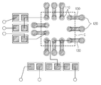
도 1은 본 발명의 일 실시예에 따른 인쇄회로기판의 일부를 나타낸 도면이다.1 is a diagram illustrating a portion of a printed circuit board according to an embodiment of the present invention.
도 1을 참조하면, 본 발명의 일 실시예에 따른 인쇄회로기판은, 칩(10)이 실장되는 칩 영역(C)을 구비하며, 실장패드(110), 프로브패드(120) 및 연결선(130)을 포함한다. 1, a printed circuit board according to an embodiment of the present invention includes a chip region C on which a
실장패드(110)는, 칩 영역(C) 내부에 형성되며, 칩 영역(C)의 둘레를 따라 복수로 형성된 BGA(ball grid array)패드이다. 실장패드(110)는 칩 영역(C)의 둘레를 따라 형성된다. 여기서, 칩 영역(C)은 칩(10)이 실장되는 영역을 의미하고, 칩 영역(C)은 칩(10)의 형태에 의해 결정되며, 인쇄회로기판 상에서 구획된다. The
도 1에 도시된 바와 같이, 11개의 실장패드(110)가 칩 영역(C)의 외곽을 따라 칩 영역(C) 내부에 형성될 수 있다. 실장패드(110)는 칩 영역(C)의 외곽부에 형성되므로, 중앙부에는 실장패드(110)가 형성되지 않고 비어있다. As shown in FIG. 1, eleven
실장패드(110)는 도 1에 도시된 바와 같이, 원형으로 형성될 수 있으나, 이에 한정되지 않으며, 다양한 형상으로 형성될 수 있다. 실장패드(110)가 원형으로 형성되는 경우, 그 직경은 약 210um일 수 있다. 칩(10)이 실장되기 위해, 실장패드(110) 상에는 솔더물질이 결합될 수 있다. The
상기 칩(10)은 IC chip 등의 다양한 칩(10)을 포함하며, 예를 들어, 모바일의 안테나 스위칭(switching) 용으로서 RF 스위칭 소자일 수 있다. 칩(10)이 실장된 후에 칩(10)의 기능 검사가 요구된다. 예를 들어, 칩(10)의 전원 핀(pin)에 전원이 공급되면 on 상태가 유지되고, 전원 공급이 차단되면 off 상태가 되는 것을 확인함으로써 칩(10)의 동작 여부를 검사할 수 있다. The
칩(10)에는 실장패드(110)와 접속되는 복수의 핀들이 구비될 수 있다. 실장패드(110)와 칩(10)의 핀은 1:1로 매칭된다. 한편, 칩(10)의 핀들은 각각의 기능을 가질 수 있다. 예를 들어, The
1pin - RF11pin - RF1
2pin - RF22pin - RF2
3pin - GND13pin - GND1
4pin - VDD(전원)4pin - VDD (power supply)
5pin - CTL15pin - CTL1
6pin - CTL26pin - CTL2
7pin - EN7pin - EN
8pin - GND28pin - GND2
9pin - RF49pin - RF4
10pin - RF310pin - RF3
11pin - RFC11pin - RFC
와 같은 기능을 가질 수 있다. 칩(10)의 검사는 각 핀들 별로 이루어지며, 모든 핀들에 대한 검사가 모두 필요할 수 있다. 다만, 핀들 중 상기의 EN(7pin)과 같은 NC핀에 대해서는 검사가 필수적인 것은 아니다. 그러나, RF1, RF2, RF3, RF4, RFC 에 대해서는 검사가 필수적이다.And the like. Inspection of the
프로브패드(120)는 칩(10) 핀의 프로빙(probing)을 위한 테스트 포인트(test point, TP)이다. 프로브패드(120)의 위치는 기설정될 수 있다. 프로브패드(120)는 칩 영역(C) 외부에, 칩 영역(C)의 둘레를 따라 형성된다. 즉, 칩 영역(C)의 외곽을 사이에 두고, 실장패드(110)와 프로브패드(120)가 서로 대향하며 형성된다. 칩 영역(C)이 사각형이라면, 이웃하는 프로브패드(120)들을 연결한 선 역시 사각형을 이루게 된다.The
프로브패드(120)는 실장패드(110)의 적어도 하나와 대응하여 형성된다. 예를 들어, 도 1에서와 같이, 실장패드(110)에 접속되는 각각의 핀들이 모두 검사가 필요한 경우라면, 실장패드(110) 전부에 대응하여 프로브패드(120)도 동일한 개수로 형성된다. 또한, 실장패드(110)의 개수와 프로브패드(120)의 개수를 동일하게 형성하더라도, 검사가 필요한 핀의 프로브패드(120)만 사용, 즉, 검사가 필요한 핀에 대해서만 검사를 실시할 수 있다. 프로브패드(120)가 복수로 형성되는 경우, 이웃하는 프로브패드(120) 간의 간격은 모두 동일하게 설계될 수 있다. 즉, 일정한 간격으로 프로브패드(120)가 형성될 수 있다.The
도 2는 본 발명의 다른 실시예에 따른 인쇄회로기판의 일부를 나타낸 도면이다. 상술한 도 1에서의 인쇄회로기판과 달리, 도 2에서의 인쇄회로기판에서는 프로브패드(120)의 개수가 실장패드(110)의 개수와 다르다. 즉, 실장패드(110)에 접속되는 핀들 중 일부에 대해서만 검사가 필요하다면, 프로브패드(120)도 검사가 필요한 핀의 실장패드(110)에 대해서만 형성될 것이다. 예를 들어, EN, GND1, GND2 에 대해서는 검사가 불필요하다면, 이에 대한 프로브패드(120)는 생략될 수 있다.2 is a diagram illustrating a portion of a printed circuit board according to another embodiment of the present invention. Unlike the printed circuit board shown in FIG. 1, the number of the
다시 도 1을 참조하면, 프로브패드(120)의 형상도 실장패드(110)와 같이 원형으로 형성될 수 있다. 또한, 프로브패드(120)의 단면적은 실장패드(110)의 단면적보다 크게 형성될 수 있다. 두 패드 모두 원형인 경우, 프로브패드(120)의 직경은 실장패드(110)의 직경보다 클 수 있다. 예를 들어, 실장패드(110)의 직경이 210um인 경우, 프로브패드(120)의 직경은 350um일 수 있다. 실장패드(110)의 경우 칩(10)이 소형화되는 추세에 따라 실장패드(110)의 크기가 함께 축소되며, 프로브패드(120)의 경우, 검사 장치의 단자 위치의 오차를 보완하기 위하여 소정의 크기를 유지하여야 하며, 칩(10)의 소형화의 영향을 적게 받기 때문에, 실장패드(110)의 크기보다 크게 형성될 수 있다.Referring again to FIG. 1, the shape of the
본 발명에서, 프로브패드(120)는 그 위치가 가변되지 않으며, 실장패드(110)와 일체화되어 형성된다. 여기서, 가변되지 않는다는 의미는, 실장패드(110)와 프로브패드(120)가 형성된 이후에 그 위치가 변하지 않는다는 것을 의미하며, 본 발명의 실시예들로부터 불변한다는 의미는 아니므로, 본 발명의 실시예들과 다른 형태로 설계될 수는 있다.In the present invention, the position of the
다만, 실장패드(110)와 함께 일체화되도록 설계되어 제작되므로, 프로브패드(120)의 위치가 고정되어, 테스트 포인트를 가변적으로 형성하던 종래의 경우에 비해, 프로브패드(120)가 형성되지 않는 불량, 설계와 다른 위치에 형성되는 형성되는 불량 등이 발생할 확률이 적어진다. Since the
한편, 연결선(130)은 서로 대응하는 실장패드(110)와 프로브패드(120)를 연결하는 전도성 라인이다. 연결선(130)은 금속으로 형성될 수 있다. 이 경우, 연결선(130)은 금(Au)을 포함하는 금속으로 형성될 수 있다. 금은 저항율이 비교적 작고, 도전율이 큰 편이다. 따라서, 금으로 형성된 연결선(130)에 의하면, 검사 시 연결선(130) 저항에 의해 발생하는 오차가 줄어들 수 있다. 한편, 연결선(130)은 금의 저항율보다 작은 저항율을 가지는 금속, 즉, 금의 도전율보다 큰 도전율을 가지는 금속으로 형성될 수 있다. 예를 들어, 은(Ag) 구리(Cu)을 포함하는 금속으로 형성될 수 있다. 또는 연결선(130)은 금, 은, 구리 등의 금속으로 도금될 수 있다.The
연결선(130)은 실장패드(110)와 프로브패드(120)를 연결하는 최단 거리의 길이(최단 길이)로 형성될 수 있다. 또한, 실장패드(110)가 칩 영역(C)의 바로 외측에 위치함으로써, 연결선(130)은 최대한 짧게 형성될 수 있다. 연결선(130)의 길이가 짧을수록 저항이 줄어들기 때문에, 검사 시 연결선(130) 저항에 의해 발생하는 오차를 감소시키기 위함이다.The
연결선(130)은 프로브패드(120)의 개수와 동일하다. 즉, 모든 실장패드(110)에 대해 프로브패드(120)가 형성된다면, 실장패드(110), 프로브패드(120) 및 연결선(130)의 개수가 모두 동일할 것이고(도 1), 실장패드(110)의 일부에 대해서만 프로브패드(120)가 형성된다면, 연결선(130)은 프로브패드(120)에 대해서만 형성될 것이다(도 2).The
연결선(130)이 복수로 형성되는 경우, 복수의 연결선(130)의 길이는 모두 동일할 수 있다. 더불어, 연결선(130)의 폭도 모두 동일할 수 있다. 이에 따라, 검사 시, 연결선(130)에서 발생하는 저항값이 모두 동일할 수 있다. When a plurality of
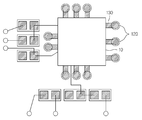
도 3을 참조하면, 본 발명의 일 실시예에 따른 칩 패키지의 일부를 나타낸 도면이다. Referring to FIG. 3, there is shown a part of a chip package according to an embodiment of the present invention.
본 발명의 일 실시예에 따른 칩 패키지는, 칩(10)과 칩(10)이 실장되는 인쇄회로기판을 포함한다. 칩(10)과 인쇄회로기판 사이에는 솔더물질이 개재될 수 있다. 칩(10)이 실장되면, 외부에서는 실장패드(110)가 보이지 않으며, 다만, 프로브패드(120)와 연결선(130)의 일부만 노출된다. 필요에 따라, 연결선(130)은 쇼트를 방지하기 위하여 레지스트 등에 의하여 커버될 수 있다.A chip package according to an embodiment of the present invention includes a printed circuit board on which a
인쇄회로기판은 칩 영역(C)이 구획되어 있으며, 칩 영역(C) 주위에 패드, 비아, 회로가 형성된다. 한편, 인쇄회로기판은 상술한 것과 같이, 칩 영역(C) 내부에 상기 칩 영역(C)의 둘레를 따라 복수로 형성된 실장패드(110), 상기 실장패드(110)의 적어도 하나에 대응하여, 상기 칩 영역(C) 외부에 상기 칩 영역(C)의 둘레를 따라 형성된 프로브패드(120), 및 서로 대응하는 상기 실장패드(110)와 상기 프로브패드(120)를 연결하는 전도성 연결선(130)을 포함할 수 있다. 연결선(130)은 상기 실장패드(110)와 상기 프로브패드(120) 사이에 최단 길이로 형성된다. The printed circuit board is divided into a chip region (C), and a pad, a via, and a circuit are formed around the chip region (C). As described above, the printed circuit board includes a plurality of mounting
상기 프로브패드(120) 및 상기 연결선(130)은 복수로 형성되는 경우, 복수의 연결선(130)의 길이는 서로 동일할 수 있다. 상기 프로브패드(120)의 단면적은 상기 실장패드(110)의 단면적보다 클 수 있다. 또한, 상기 연결선(130)은 저항율이 금의 저항율 이하인 금속으로 형성될 수 있다. 이외의 설명들에 대해서는 상술한 바와 동일하므로 생략한다.When a plurality of
상술한 바와 같이, 칩 패키지용 인쇄회로기판 설계 시 프로브패드를 칩 영역 외측에 고정적으로 포함시키면, 칩 검사에 필요한 테스트 포인트의 미삽입, 오삽입 등의 불량이 야기되지 않는다. 또한, 인쇄회로기판의 회로와 프로브패드를 함께 설계할 수 있으므로, 회로와 테스트 포인트에 대한 인쇄회로기판의 공간 활용이 효율적이고 체계적으로 이루어질 수 있다. 한편, 프로브패드의 위치가 고정되어 검사 지그의 위치도 고정될 수 있으므로, 다량의 인쇄회로기판의 칩을 효율적으로 검사할 수 있다.As described above, when the probe pads are fixedly provided outside the chip area in the design of the printed circuit board for the chip package, defects such as non-insertion and mis-insertion of test points necessary for chip inspection are not caused. In addition, since the circuit of the printed circuit board and the probe pad can be designed together, space utilization of the printed circuit board for the circuit and the test point can be efficiently and systematically performed. On the other hand, since the positions of the probe pads can be fixed and the positions of the inspection jigs can be fixed, a large number of chips of the printed circuit board can be efficiently inspected.
이상, 본 발명의 일 실시예에 대하여 설명하였으나, 해당 기술 분야에서 통상의 지식을 가진 자라면 특허청구범위에 기재된 본 발명의 사상으로부터 벗어나지 않는 범위 내에서, 구성 요소의 부가, 변경, 삭제 또는 추가 등에 의해 본 발명을 다양하게 수정 및 변경시킬 수 있을 것이며, 이 또한 본 발명의 권리범위 내에 포함된다고 할 것이다.It will be apparent to those skilled in the art that various modifications and variations can be made in the present invention without departing from the spirit of the invention as set forth in the appended claims. The present invention can be variously modified and changed by those skilled in the art, and it is also within the scope of the present invention.
10: 칩
110: 실장패드
120: 프로브패드
130: 연결선
C: 칩 영역10: Chip
110: mounting pad
120: Probe pad
130: connection line
C: chip area
Claims (10)
상기 실장패드의 적어도 하나에 대응하여, 상기 칩 영역 외부에 상기 칩 영역의 둘레를 따라 형성된 프로브패드; 및
서로 대응하는 상기 실장패드와 상기 프로브패드를 연결하는 전도성 연결선을 포함하는 인쇄회로기판.
A plurality of mounting pads formed along the periphery of the chip region in the chip region;
A probe pad formed on the periphery of the chip area outside the chip area, corresponding to at least one of the mounting pads; And
And a conductive connection line connecting the mounting pads and the probe pads corresponding to each other.
상기 연결선은 상기 실장패드와 상기 프로브패드 사이에 최단 길이로 형성되는 인쇄회로기판.
The method according to claim 1,
Wherein the connection line is formed at a shortest length between the mounting pad and the probe pad.
상기 프로브패드 및 상기 연결선은 복수로 형성되고,
복수의 상기 연결선의 길이는 서로 동일한 인쇄회로기판.
The method according to claim 1,
Wherein the probe pad and the connection line are formed in plural numbers,
Wherein the plurality of connection lines have the same length.
상기 프로브패드의 단면적은 상기 실장패드의 단면적보다 큰 인쇄회로기판.
The method according to claim 1,
Wherein a cross-sectional area of the probe pad is larger than a cross-sectional area of the mounting pad.
상기 연결선은 저항율이 금(Au)의 저항율 이하인 금속으로 형성되는 인쇄회로기판.
The method according to claim 1,
Wherein the connecting line is formed of a metal whose resistivity is lower than that of gold (Au).
상기 인쇄회로기판은,
칩 영역 내부에 상기 칩 영역의 둘레를 따라 복수로 형성된 실장패드;
상기 실장패드의 적어도 하나에 대응하여, 상기 칩 영역 외부에 상기 칩 영역의 둘레를 따라 형성된 프로브패드; 및
서로 대응하는 상기 실장패드와 상기 프로브패드를 연결하는 전도성 연결선을 포함하는 칩 패키지.
chip; And a printed circuit board having a chip area on which the chip is mounted,
Wherein the printed circuit board includes:
A plurality of mounting pads formed along the periphery of the chip region in the chip region;
A probe pad formed on the periphery of the chip area outside the chip area, corresponding to at least one of the mounting pads; And
And a conductive connection line connecting the mounting pads and the probe pads corresponding to each other.
상기 연결선은 상기 실장패드와 상기 프로브패드 사이에 최단 길이로 형성되는 칩 패키지.
The method according to claim 6,
Wherein the connection line is formed at a shortest length between the mounting pad and the probe pad.
상기 프로브패드 및 상기 연결선은 복수로 형성되고,
복수의 상기 연결선의 길이는 서로 동일한 칩 패키지.
The method according to claim 6,
Wherein the probe pad and the connection line are formed in plural numbers,
Wherein the plurality of connection lines have the same length.
상기 프로브패드의 단면적은 상기 실장패드의 단면적보다 큰 칩 패키지.
The method according to claim 6,
Wherein a cross-sectional area of the probe pad is larger than a cross-sectional area of the mounting pad.
상기 연결선은 저항율이 금(Au)의 저항율 이하인 금속으로 형성되는 칩 패키지.
The method according to claim 6,
Wherein the connecting line is formed of a metal whose resistivity is lower than that of gold (Au).
Priority Applications (1)
| Application Number | Priority Date | Filing Date | Title |
|---|---|---|---|
| KR1020150114616A KR20170020002A (en) | 2015-08-13 | 2015-08-13 | Printed circuit board and chip package having the same |
Applications Claiming Priority (1)
| Application Number | Priority Date | Filing Date | Title |
|---|---|---|---|
| KR1020150114616A KR20170020002A (en) | 2015-08-13 | 2015-08-13 | Printed circuit board and chip package having the same |
Publications (1)
| Publication Number | Publication Date |
|---|---|
| KR20170020002A true KR20170020002A (en) | 2017-02-22 |
Family
ID=58314785
Family Applications (1)
| Application Number | Title | Priority Date | Filing Date |
|---|---|---|---|
| KR1020150114616A Ceased KR20170020002A (en) | 2015-08-13 | 2015-08-13 | Printed circuit board and chip package having the same |
Country Status (1)
| Country | Link |
|---|---|
| KR (1) | KR20170020002A (en) |
Cited By (1)
| Publication number | Priority date | Publication date | Assignee | Title |
|---|---|---|---|---|
| KR20190091969A (en) * | 2018-01-30 | 2019-08-07 | 주식회사 엘지화학 | Method for manufacturing printed circuit board with test points and printed circuit board using thereof |
Citations (1)
| Publication number | Priority date | Publication date | Assignee | Title |
|---|---|---|---|---|
| KR20120031147A (en) | 2010-09-22 | 2012-03-30 | 세이코 인스트루 가부시키가이샤 | Bga semiconductor package and manufacturing method thereof |
-
2015
- 2015-08-13 KR KR1020150114616A patent/KR20170020002A/en not_active Ceased
Patent Citations (1)
| Publication number | Priority date | Publication date | Assignee | Title |
|---|---|---|---|---|
| KR20120031147A (en) | 2010-09-22 | 2012-03-30 | 세이코 인스트루 가부시키가이샤 | Bga semiconductor package and manufacturing method thereof |
Cited By (4)
| Publication number | Priority date | Publication date | Assignee | Title |
|---|---|---|---|---|
| KR20190091969A (en) * | 2018-01-30 | 2019-08-07 | 주식회사 엘지화학 | Method for manufacturing printed circuit board with test points and printed circuit board using thereof |
| WO2019151752A1 (en) * | 2018-01-30 | 2019-08-08 | 주식회사 엘지화학 | Method for manufacturing printed circuit board having test point, and printed circuit board manufactured thereby |
| CN110870390A (en) * | 2018-01-30 | 2020-03-06 | 株式会社Lg化学 | Method for manufacturing a printed circuit board with test points and printed circuit board manufactured therefrom |
| US10966313B2 (en) | 2018-01-30 | 2021-03-30 | Lg Chem, Ltd. | Method for manufacturing printed circuit board having test point, and printed circuit board manufactured thereby |
Similar Documents
| Publication | Publication Date | Title |
|---|---|---|
| US10475760B2 (en) | Semiconductor device | |
| KR100236633B1 (en) | Printed circuit board strip structure and semiconductor package manufacturing method using the same | |
| KR20100052959A (en) | Interface structure for wafer test equipments | |
| JP2011122924A (en) | Semiconductor device and method of manufacturing the same | |
| US8115321B2 (en) | Separate probe and bond regions of an integrated circuit | |
| US20050248011A1 (en) | Flip chip semiconductor package for testing bump and method of fabricating the same | |
| JP2009278051A (en) | Semiconductor package | |
| US9110128B1 (en) | IC package for pin counts less than test requirements | |
| US20130292165A1 (en) | Circuit board | |
| KR20170020002A (en) | Printed circuit board and chip package having the same | |
| KR20040080739A (en) | Semiconductor chip having test pads and tape carrier package using thereof | |
| TWI598596B (en) | Testing probe card for integrated circuit | |
| US20080303177A1 (en) | Bonding pad structure | |
| JP2016514367A (en) | Package substrate with test pads on fine pitch trace | |
| JP5666366B2 (en) | Manufacturing method of semiconductor device | |
| JP4002143B2 (en) | Manufacturing method of semiconductor device | |
| US20130242518A1 (en) | Chip assembly and chip assembling method | |
| KR100377469B1 (en) | Clamp for Bonding Wire of Ball Grid Array Semiconductor Packages and Method for Checking the Bonding Wire Using the same | |
| US7064421B2 (en) | Wire bonding package | |
| TW202011031A (en) | Integrated circuit socket with at least one of probes electrically connected to a detection printed circuit for electrically connecting an integrated circuit, the detection printed circuit, and an integrated circuit test board | |
| KR20080000879A (en) | Vijay semiconductor chip package and inspection method thereof | |
| KR100718324B1 (en) | Bluetooth Module Printed Circuit Board | |
| US20090189628A1 (en) | Reworkable bonding pad layout and debug method thereof | |
| US20130153278A1 (en) | Ball grid array package and method of manufacturing the same | |
| JP4408748B2 (en) | Manufacturing method of semiconductor device |
Legal Events
| Date | Code | Title | Description |
|---|---|---|---|
| PA0109 | Patent application |
St.27 status event code: A-0-1-A10-A12-nap-PA0109 |
|
| PG1501 | Laying open of application |
St.27 status event code: A-1-1-Q10-Q12-nap-PG1501 |
|
| P22-X000 | Classification modified |
St.27 status event code: A-2-2-P10-P22-nap-X000 |
|
| R17-X000 | Change to representative recorded |
St.27 status event code: A-3-3-R10-R17-oth-X000 |
|
| R18-X000 | Changes to party contact information recorded |
St.27 status event code: A-3-3-R10-R18-oth-X000 |
|
| A201 | Request for examination | ||
| PA0201 | Request for examination |
St.27 status event code: A-1-2-D10-D11-exm-PA0201 |
|
| E902 | Notification of reason for refusal | ||
| PE0902 | Notice of grounds for rejection |
St.27 status event code: A-1-2-D10-D21-exm-PE0902 |
|
| E13-X000 | Pre-grant limitation requested |
St.27 status event code: A-2-3-E10-E13-lim-X000 |
|
| P11-X000 | Amendment of application requested |
St.27 status event code: A-2-2-P10-P11-nap-X000 |
|
| P13-X000 | Application amended |
St.27 status event code: A-2-2-P10-P13-nap-X000 |
|
| E601 | Decision to refuse application | ||
| PE0601 | Decision on rejection of patent |
St.27 status event code: N-2-6-B10-B15-exm-PE0601 |
|
| P22-X000 | Classification modified |
St.27 status event code: A-2-2-P10-P22-nap-X000 |