KR20170067002A - 전자 빔을 이용한 도전성 나노와이어 네트워크의 제조방법, 이를 적용한 투명 전극 및 전자 장치 - Google Patents
전자 빔을 이용한 도전성 나노와이어 네트워크의 제조방법, 이를 적용한 투명 전극 및 전자 장치 Download PDFInfo
- Publication number
- KR20170067002A KR20170067002A KR1020150173336A KR20150173336A KR20170067002A KR 20170067002 A KR20170067002 A KR 20170067002A KR 1020150173336 A KR1020150173336 A KR 1020150173336A KR 20150173336 A KR20150173336 A KR 20150173336A KR 20170067002 A KR20170067002 A KR 20170067002A
- Authority
- KR
- South Korea
- Prior art keywords
- electron beam
- nanowire network
- nanowires
- conductive
- nanowire
- Prior art date
- Legal status (The legal status is an assumption and is not a legal conclusion. Google has not performed a legal analysis and makes no representation as to the accuracy of the status listed.)
- Ceased
Links
Images



Classifications
-
- H—ELECTRICITY
- H01—ELECTRIC ELEMENTS
- H01B—CABLES; CONDUCTORS; INSULATORS; SELECTION OF MATERIALS FOR THEIR CONDUCTIVE, INSULATING OR DIELECTRIC PROPERTIES
- H01B13/00—Apparatus or processes specially adapted for manufacturing conductors or cables
- H01B13/0026—Apparatus for manufacturing conducting or semi-conducting layers, e.g. deposition of metal
-
- H—ELECTRICITY
- H05—ELECTRIC TECHNIQUES NOT OTHERWISE PROVIDED FOR
- H05K—PRINTED CIRCUITS; CASINGS OR CONSTRUCTIONAL DETAILS OF ELECTRIC APPARATUS; MANUFACTURE OF ASSEMBLAGES OF ELECTRICAL COMPONENTS
- H05K3/00—Apparatus or processes for manufacturing printed circuits
- H05K3/02—Apparatus or processes for manufacturing printed circuits in which the conductive material is applied to the surface of the insulating support and is thereafter removed from such areas of the surface which are not intended for current conducting or shielding
-
- B—PERFORMING OPERATIONS; TRANSPORTING
- B82—NANOTECHNOLOGY
- B82Y—SPECIFIC USES OR APPLICATIONS OF NANOSTRUCTURES; MEASUREMENT OR ANALYSIS OF NANOSTRUCTURES; MANUFACTURE OR TREATMENT OF NANOSTRUCTURES
- B82Y20/00—Nanooptics, e.g. quantum optics or photonic crystals
-
- B—PERFORMING OPERATIONS; TRANSPORTING
- B82—NANOTECHNOLOGY
- B82Y—SPECIFIC USES OR APPLICATIONS OF NANOSTRUCTURES; MEASUREMENT OR ANALYSIS OF NANOSTRUCTURES; MANUFACTURE OR TREATMENT OF NANOSTRUCTURES
- B82Y40/00—Manufacture or treatment of nanostructures
-
- G—PHYSICS
- G06—COMPUTING OR CALCULATING; COUNTING
- G06F—ELECTRIC DIGITAL DATA PROCESSING
- G06F3/00—Input arrangements for transferring data to be processed into a form capable of being handled by the computer; Output arrangements for transferring data from processing unit to output unit, e.g. interface arrangements
- G06F3/01—Input arrangements or combined input and output arrangements for interaction between user and computer
- G06F3/03—Arrangements for converting the position or the displacement of a member into a coded form
- G06F3/041—Digitisers, e.g. for touch screens or touch pads, characterised by the transducing means
-
- H—ELECTRICITY
- H01—ELECTRIC ELEMENTS
- H01B—CABLES; CONDUCTORS; INSULATORS; SELECTION OF MATERIALS FOR THEIR CONDUCTIVE, INSULATING OR DIELECTRIC PROPERTIES
- H01B1/00—Conductors or conductive bodies characterised by the conductive materials; Selection of materials as conductors
- H01B1/02—Conductors or conductive bodies characterised by the conductive materials; Selection of materials as conductors mainly consisting of metals or alloys
-
- H—ELECTRICITY
- H01—ELECTRIC ELEMENTS
- H01B—CABLES; CONDUCTORS; INSULATORS; SELECTION OF MATERIALS FOR THEIR CONDUCTIVE, INSULATING OR DIELECTRIC PROPERTIES
- H01B1/00—Conductors or conductive bodies characterised by the conductive materials; Selection of materials as conductors
- H01B1/20—Conductive material dispersed in non-conductive organic material
- H01B1/22—Conductive material dispersed in non-conductive organic material the conductive material comprising metals or alloys
-
- H—ELECTRICITY
- H01—ELECTRIC ELEMENTS
- H01B—CABLES; CONDUCTORS; INSULATORS; SELECTION OF MATERIALS FOR THEIR CONDUCTIVE, INSULATING OR DIELECTRIC PROPERTIES
- H01B5/00—Non-insulated conductors or conductive bodies characterised by their form
- H01B5/14—Non-insulated conductors or conductive bodies characterised by their form comprising conductive layers or films on insulating-supports
-
- H—ELECTRICITY
- H01—ELECTRIC ELEMENTS
- H01B—CABLES; CONDUCTORS; INSULATORS; SELECTION OF MATERIALS FOR THEIR CONDUCTIVE, INSULATING OR DIELECTRIC PROPERTIES
- H01B7/00—Insulated conductors or cables characterised by their form
-
- H01L31/022425—
-
- H01L31/022466—
-
- H—ELECTRICITY
- H05—ELECTRIC TECHNIQUES NOT OTHERWISE PROVIDED FOR
- H05K—PRINTED CIRCUITS; CASINGS OR CONSTRUCTIONAL DETAILS OF ELECTRIC APPARATUS; MANUFACTURE OF ASSEMBLAGES OF ELECTRICAL COMPONENTS
- H05K1/00—Printed circuits
- H05K1/02—Details
- H05K1/09—Use of materials for the conductive, e.g. metallic pattern
- H05K1/092—Dispersed materials, e.g. conductive pastes or inks
- H05K1/097—Inks comprising nanoparticles and specially adapted for being sintered at low temperature
-
- H—ELECTRICITY
- H05—ELECTRIC TECHNIQUES NOT OTHERWISE PROVIDED FOR
- H05K—PRINTED CIRCUITS; CASINGS OR CONSTRUCTIONAL DETAILS OF ELECTRIC APPARATUS; MANUFACTURE OF ASSEMBLAGES OF ELECTRICAL COMPONENTS
- H05K2201/00—Indexing scheme relating to printed circuits covered by H05K1/00
- H05K2201/02—Fillers; Particles; Fibers; Reinforcement materials
- H05K2201/0203—Fillers and particles
- H05K2201/0242—Shape of an individual particle
- H05K2201/026—Nanotubes or nanowires
-
- Y—GENERAL TAGGING OF NEW TECHNOLOGICAL DEVELOPMENTS; GENERAL TAGGING OF CROSS-SECTIONAL TECHNOLOGIES SPANNING OVER SEVERAL SECTIONS OF THE IPC; TECHNICAL SUBJECTS COVERED BY FORMER USPC CROSS-REFERENCE ART COLLECTIONS [XRACs] AND DIGESTS
- Y10—TECHNICAL SUBJECTS COVERED BY FORMER USPC
- Y10S—TECHNICAL SUBJECTS COVERED BY FORMER USPC CROSS-REFERENCE ART COLLECTIONS [XRACs] AND DIGESTS
- Y10S977/00—Nanotechnology
- Y10S977/70—Nanostructure
- Y10S977/762—Nanowire or quantum wire, i.e. axially elongated structure having two dimensions of 100 nm or less
-
- Y—GENERAL TAGGING OF NEW TECHNOLOGICAL DEVELOPMENTS; GENERAL TAGGING OF CROSS-SECTIONAL TECHNOLOGIES SPANNING OVER SEVERAL SECTIONS OF THE IPC; TECHNICAL SUBJECTS COVERED BY FORMER USPC CROSS-REFERENCE ART COLLECTIONS [XRACs] AND DIGESTS
- Y10—TECHNICAL SUBJECTS COVERED BY FORMER USPC
- Y10S—TECHNICAL SUBJECTS COVERED BY FORMER USPC CROSS-REFERENCE ART COLLECTIONS [XRACs] AND DIGESTS
- Y10S977/00—Nanotechnology
- Y10S977/70—Nanostructure
- Y10S977/81—Of specified metal or metal alloy composition
-
- Y—GENERAL TAGGING OF NEW TECHNOLOGICAL DEVELOPMENTS; GENERAL TAGGING OF CROSS-SECTIONAL TECHNOLOGIES SPANNING OVER SEVERAL SECTIONS OF THE IPC; TECHNICAL SUBJECTS COVERED BY FORMER USPC CROSS-REFERENCE ART COLLECTIONS [XRACs] AND DIGESTS
- Y10—TECHNICAL SUBJECTS COVERED BY FORMER USPC
- Y10S—TECHNICAL SUBJECTS COVERED BY FORMER USPC CROSS-REFERENCE ART COLLECTIONS [XRACs] AND DIGESTS
- Y10S977/00—Nanotechnology
- Y10S977/902—Specified use of nanostructure
- Y10S977/932—Specified use of nanostructure for electronic or optoelectronic application
- Y10S977/949—Radiation emitter using nanostructure
- Y10S977/95—Electromagnetic energy
-
- Y—GENERAL TAGGING OF NEW TECHNOLOGICAL DEVELOPMENTS; GENERAL TAGGING OF CROSS-SECTIONAL TECHNOLOGIES SPANNING OVER SEVERAL SECTIONS OF THE IPC; TECHNICAL SUBJECTS COVERED BY FORMER USPC CROSS-REFERENCE ART COLLECTIONS [XRACs] AND DIGESTS
- Y10—TECHNICAL SUBJECTS COVERED BY FORMER USPC
- Y10S—TECHNICAL SUBJECTS COVERED BY FORMER USPC CROSS-REFERENCE ART COLLECTIONS [XRACs] AND DIGESTS
- Y10S977/00—Nanotechnology
- Y10S977/902—Specified use of nanostructure
- Y10S977/932—Specified use of nanostructure for electronic or optoelectronic application
- Y10S977/953—Detector using nanostructure
-
- Y—GENERAL TAGGING OF NEW TECHNOLOGICAL DEVELOPMENTS; GENERAL TAGGING OF CROSS-SECTIONAL TECHNOLOGIES SPANNING OVER SEVERAL SECTIONS OF THE IPC; TECHNICAL SUBJECTS COVERED BY FORMER USPC CROSS-REFERENCE ART COLLECTIONS [XRACs] AND DIGESTS
- Y10—TECHNICAL SUBJECTS COVERED BY FORMER USPC
- Y10S—TECHNICAL SUBJECTS COVERED BY FORMER USPC CROSS-REFERENCE ART COLLECTIONS [XRACs] AND DIGESTS
- Y10S977/00—Nanotechnology
- Y10S977/902—Specified use of nanostructure
- Y10S977/932—Specified use of nanostructure for electronic or optoelectronic application
- Y10S977/953—Detector using nanostructure
- Y10S977/954—Of radiant energy
Landscapes
- Engineering & Computer Science (AREA)
- Chemical & Material Sciences (AREA)
- Nanotechnology (AREA)
- Microelectronics & Electronic Packaging (AREA)
- Manufacturing & Machinery (AREA)
- Physics & Mathematics (AREA)
- Crystallography & Structural Chemistry (AREA)
- Life Sciences & Earth Sciences (AREA)
- General Physics & Mathematics (AREA)
- Dispersion Chemistry (AREA)
- Condensed Matter Physics & Semiconductors (AREA)
- Biophysics (AREA)
- Optics & Photonics (AREA)
- General Engineering & Computer Science (AREA)
- Conductive Materials (AREA)
- Theoretical Computer Science (AREA)
- Manufacturing Of Electric Cables (AREA)
- Human Computer Interaction (AREA)
- Spectroscopy & Molecular Physics (AREA)
- Sustainable Development (AREA)
- Sustainable Energy (AREA)
Abstract
Description
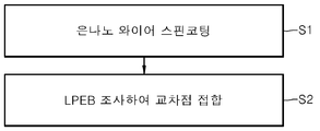
도 2는 본 발명의 실시예에 따른 전자 빔을 이용한 도전성 나노와이어 네트워크의 제조방법을 나타낸 도면이다.
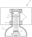
도 3은 본 발명의 실시예에 따른 제조방법에 사용된 대형 펄스 전자 빔 조사장치의 개략도이다.
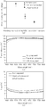
도 4는 본 발명의 실시예에 따른 전자 빔을 이용한 도전성 나노와이어 네트워크의 제조방법과 종래의 제조방법에 따라 각각 접합된 은 나노 네트워크의 특성을 비교하여 나타낸 그래프이다.
도 5는 본 발명의 실시예에 따른 전자 빔을 이용한 도전성 나노와이어 네트워크의 제조방법과 종래의 제조방법에 따른 주기적인 밴딩 시험 결과를 나타낸 그래프이다.
도 6은 본 발명의 실시예에 따른 은 나노 네트워크를 나타낸 SEM 사진이다.
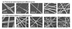
도 7은 본 발명의 실시예에 따른 전자 빔을 이용한 도전성 나노 와이어 네트워크의 제조방법과 종래의 제조방법에 따른 은나노 네트워크를 비교한 SEM 사진이다.
Claims (16)
- 도전성 나노 와이어들을 이용하여 나노 와이어 네트워크를 형성하는 단계와;
상기 나노 와이어 네트워크에 전자빔을 조사하여 상기 도전성 나노 와이어들의 교차점을 접합시키는 단계를 포함하는 전자 빔을 이용한 도전성 나노와이어 네트워크의 제조방법. - 청구항 1에 있어서,
상기 전자빔은 대형 펄스 전자 빔(Large pulsed electron beam)을 사용하는 전자 빔을 이용한 도전성 나노와이어 네트워크의 제조방법. - 청구항 2에 있어서,
상기 대형 펄스 전자빔의 가속 전압은 5kV이하로 설정하는 전자 빔을 이용한 도전성 나노와이어 네트워크의 제조방법. - 청구항 2에 있어서,
상기 대형 펄스 전자빔의 펄스의 파장은 0.1 Hz 내지 0.2 Hz 범위인 도전성 나노와이어 네트워크의 제조방법. - 청구항 1에 있어서,
상기 전자빔의 지름은 50 mm 내지 80 mm 범위인 도전성 나노 와이어 네트워크의 제조방법. - 청구항 1에 있어서,
상기 도전성 나노 와이어는, 은 나노 와이어를 포함하는 전자 빔을 이용한 도전성 나노와이어 네트워크의 제조방법. - 청구항 6에 있어서,
상기 나노 와이어 네트워크를 형성하는 단계는,
이소프로필 알코올(IPA)과 상기 은 나노 와이어가 혼합된 현탁액을 스핀 코팅하여 형성하는 도전성 나노 와이어 네트워크의 제조방법. - 청구항 7에 있어서,
상기 은 나노 와이어의 길이는 20 내지 30㎛이고, 직경은 30 내지 40nm인 도전성 나노 와이어 네트워크의 제조방법. - 베이스 기재 상에서 도전성 나노 와이어들이 나노 와이어 네트워크를 형성하고, 상기 나노 와이어 네트워크에 전자빔을 조사하여 상기 도전성 나노 와이어들의 교차점이 접합된 투명 전극.
- 청구항 9에 있어서,
상기 도전성 나노 와이어들은, 대형 펄스 전자 빔(Large pulsed electron beam)을 사용하여 접합된 투명 전극. - 청구항 10에 있어서,
상기 도전성 나노 와이어들은, 상기 대형 펄스 전자 빔의 가속 전압이 5kV이하로 조사되어 접합된 투명 전극. - 청구항 11에 있어서,
상기 도전성 나노 와이어들은, 상기 대형 펄스 전자빔의 펄스의 파장이 0.1 Hz 내지 0.2 Hz 범위로 조사되어 접합된 투명 전극. - 청구항 12에 있어서,
상기 도전성 나노 와이어들은, 상기 대형 펄스 전자빔의 지름이 50 mm 내지 80 mm 범위로 조사되어 접합된 투명 전극. - 청구항 9에 있어서,
상기 도전성 나노 와이어는, 은 나노 와이어를 포함하는 투명 전극. - 베이스 기재 상에서 도전성 나노 와이어들이 나노 와이어 네트워크를 형성하고, 상기 나노 와이어 네트워크에 전자빔을 조사하여 상기 도전성 나노 와이어들의 교차점이 접합된 투명 전극을 포함하는 전자 장치.
- 청구항 15에 있어서,
상기 전자 장치는, 터치 패널, LED, 솔라셀 또는 센서를 포함하는 전자 장치.
Priority Applications (3)
| Application Number | Priority Date | Filing Date | Title |
|---|---|---|---|
| KR1020150173336A KR20170067002A (ko) | 2015-12-07 | 2015-12-07 | 전자 빔을 이용한 도전성 나노와이어 네트워크의 제조방법, 이를 적용한 투명 전극 및 전자 장치 |
| PCT/KR2016/011628 WO2017099345A1 (ko) | 2015-12-07 | 2016-10-17 | 전자 빔을 이용한 도전성 나노와이어 네트워크의 제조방법, 이를 적용한 투명 전극 및 전자 장치 |
| US15/346,729 US10085339B2 (en) | 2015-12-07 | 2016-11-09 | Method of manufacturing electroconductive nanowire network using electron beam, transparent electrode and electronic device using the same |
Applications Claiming Priority (1)
| Application Number | Priority Date | Filing Date | Title |
|---|---|---|---|
| KR1020150173336A KR20170067002A (ko) | 2015-12-07 | 2015-12-07 | 전자 빔을 이용한 도전성 나노와이어 네트워크의 제조방법, 이를 적용한 투명 전극 및 전자 장치 |
Publications (1)
| Publication Number | Publication Date |
|---|---|
| KR20170067002A true KR20170067002A (ko) | 2017-06-15 |
Family
ID=58799322
Family Applications (1)
| Application Number | Title | Priority Date | Filing Date |
|---|---|---|---|
| KR1020150173336A Ceased KR20170067002A (ko) | 2015-12-07 | 2015-12-07 | 전자 빔을 이용한 도전성 나노와이어 네트워크의 제조방법, 이를 적용한 투명 전극 및 전자 장치 |
Country Status (3)
| Country | Link |
|---|---|
| US (1) | US10085339B2 (ko) |
| KR (1) | KR20170067002A (ko) |
| WO (1) | WO2017099345A1 (ko) |
Cited By (1)
| Publication number | Priority date | Publication date | Assignee | Title |
|---|---|---|---|---|
| KR20200077479A (ko) * | 2020-06-19 | 2020-06-30 | 한국화학연구원 | 은 나노선-그래핀 복합 나노박막 및 이의 제조방법 |
Families Citing this family (6)
| Publication number | Priority date | Publication date | Assignee | Title |
|---|---|---|---|---|
| CN110083279A (zh) * | 2019-05-07 | 2019-08-02 | 业成科技(成都)有限公司 | 透明导电材料、触控结构及触控装置 |
| CN110844879B (zh) * | 2019-11-14 | 2020-09-22 | 常州大学 | 一种非晶纳米线与多孔薄膜的原位可操控键合方法 |
| CN113106430A (zh) * | 2021-03-30 | 2021-07-13 | 重庆烯宇新材料科技有限公司 | 一种促进纳米银线结点焊接成连续低阻导电网络的化学方法 |
| CN113707368A (zh) * | 2021-09-06 | 2021-11-26 | 石家庄铁道大学 | 一种耐高温透明柔性导电材料及其制备方法 |
| CN115360263B (zh) * | 2022-08-19 | 2025-05-06 | 陕西科技大学 | 单晶硅上3C-SiC纳米线功能复合网络薄膜及其制备方法和应用 |
| CN116037915A (zh) * | 2022-12-30 | 2023-05-02 | 常州大学 | 一种高能电子束非热诱导PVP@Ag纳米线加工的方法 |
Family Cites Families (11)
| Publication number | Priority date | Publication date | Assignee | Title |
|---|---|---|---|---|
| DE19541510C2 (de) | 1995-11-08 | 1999-08-12 | Karlsruhe Forschzent | Gepulste Elektronenstrahlquelle und deren Verwendung |
| KR101885376B1 (ko) * | 2011-02-11 | 2018-08-06 | 한국과학기술원 | 은 나노 와이어를 이용한 투명전극 및 그 제조 방법 |
| JP2013109460A (ja) * | 2011-11-18 | 2013-06-06 | Shin Etsu Polymer Co Ltd | 透明配線シート |
| US9603242B2 (en) * | 2011-12-21 | 2017-03-21 | 3M Innovative Properties Company | Laser patterning of silver nanowire-based transparent electrically conducting coatings |
| KR101386362B1 (ko) * | 2012-09-27 | 2014-04-16 | 한국과학기술원 | 은 나노와이어 네트워크―그래핀 적층형 투명전극 소재, 그 제조 방법 및 이를 포함하는 투명전극 |
| KR102153428B1 (ko) | 2013-02-20 | 2020-09-08 | 도오쿄 인스티튜드 오브 테크놀로지 | 도전성 나노와이어 네트워크 및 이것을 이용한 도전성 기판 및 투명전극, 그리고 그들의 제조 방법 |
| KR101582376B1 (ko) * | 2013-06-07 | 2016-01-04 | 주식회사 제낙스 | 전극, 이의 제조 방법 및 이를 이용한 전지 |
| KR101484771B1 (ko) * | 2013-07-31 | 2015-01-22 | 한국과학기술원 | 은 나노와이어를 이용한 전극소자 및 그 제조 방법 |
| KR101440396B1 (ko) * | 2014-02-20 | 2014-09-18 | 주식회사 인포비온 | 전도성 나노 와이어를 이용한 투명 도전막의 제조 방법 |
| US9808781B2 (en) * | 2014-08-08 | 2017-11-07 | The University Of Hong Kong | Conductive metal networks including metal nanowires and metal nanoparticles and methods of fabricating the same |
| JP6379018B2 (ja) * | 2014-11-20 | 2018-08-22 | 株式会社日立ハイテクノロジーズ | 荷電粒子線装置および検査方法 |
-
2015
- 2015-12-07 KR KR1020150173336A patent/KR20170067002A/ko not_active Ceased
-
2016
- 2016-10-17 WO PCT/KR2016/011628 patent/WO2017099345A1/ko not_active Ceased
- 2016-11-09 US US15/346,729 patent/US10085339B2/en active Active
Cited By (1)
| Publication number | Priority date | Publication date | Assignee | Title |
|---|---|---|---|---|
| KR20200077479A (ko) * | 2020-06-19 | 2020-06-30 | 한국화학연구원 | 은 나노선-그래핀 복합 나노박막 및 이의 제조방법 |
Also Published As
| Publication number | Publication date |
|---|---|
| US20170164467A1 (en) | 2017-06-08 |
| US10085339B2 (en) | 2018-09-25 |
| WO2017099345A1 (ko) | 2017-06-15 |
Similar Documents
| Publication | Publication Date | Title |
|---|---|---|
| KR20170067002A (ko) | 전자 빔을 이용한 도전성 나노와이어 네트워크의 제조방법, 이를 적용한 투명 전극 및 전자 장치 | |
| Jiu et al. | Strongly adhesive and flexible transparent silver nanowire conductive films fabricated with a high-intensity pulsed light technique | |
| Chae et al. | Double-sided graphene oxide encapsulated silver nanowire transparent electrode with improved chemical and electrical stability | |
| KR101637920B1 (ko) | 투명필름히터 및 그의 제조방법 | |
| CN109920603B (zh) | 一种提高银纳米线透明导电膜导电性的装置及方法 | |
| US8932898B2 (en) | Deposition and post-processing techniques for transparent conductive films | |
| US20100051101A1 (en) | Electrode of flexible dye-sensitized solar cell, manufacturing method thereof and flexible dye-sensitized solar cell | |
| WO2016068602A1 (ko) | 투명 전도체 및 이의 제조방법 | |
| Wang et al. | Customizable stretchable transparent electrodes based on AgNW/CNT hybrids via tailoring sizes of building blocks | |
| Ko et al. | Ag nanowires via solution process and localized reduction of Ag ions for next-generation transparent conductive electrodes | |
| KR101484771B1 (ko) | 은 나노와이어를 이용한 전극소자 및 그 제조 방법 | |
| CN106513959B (zh) | 一种银纳米线焊接方法 | |
| Li et al. | Improving edge quality and optical transmittance of Ag films on glass substrates by selective nanosecond pulsed laser ablation using various scanning methods | |
| WO2011007297A2 (en) | Method for producing structured conductive layers | |
| KR101627422B1 (ko) | 복합광원을 이용한 금속 나노와이어와 그래핀 옥사이드 기반의 투명전극 및 이의 제조방법 | |
| US20170133129A1 (en) | Method of using carbon nanotubes to fabricate transparent conductive film | |
| CN105845842A (zh) | 导体、电子器件、和制造导体的方法 | |
| TWI376827B (en) | Radiation emitting device and method of manufacturing radiation emitting device | |
| Jung et al. | Microwave welding of silver nanowires for highly transparent conductive electrodes | |
| TW201521263A (zh) | 藉由將銀除潤之柵極的製造法 | |
| CN116037915A (zh) | 一种高能电子束非热诱导PVP@Ag纳米线加工的方法 | |
| KR101913335B1 (ko) | 네트워크 구조가 강화된 나노 와이어 투명 전극 제조방법 및 이에 의해 제조된 투명 전극 필름 | |
| CN103366644A (zh) | 白炽光源及白炽光源显示装置的制备方法 | |
| Jang et al. | Improvement of Contact Resistance Between Each Silver Nanowire and Thermal Stability of Silver Nanowire Transparent Electrodes by Electrodeposition | |
| KR101828578B1 (ko) | 금속 나노와이어와 금속입자가 용접된 금속복합구조체의 제조방법 |
Legal Events
| Date | Code | Title | Description |
|---|---|---|---|
| A201 | Request for examination | ||
| PA0109 | Patent application |
St.27 status event code: A-0-1-A10-A12-nap-PA0109 |
|
| PA0201 | Request for examination |
St.27 status event code: A-1-2-D10-D11-exm-PA0201 |
|
| PN2301 | Change of applicant |
St.27 status event code: A-3-3-R10-R13-asn-PN2301 St.27 status event code: A-3-3-R10-R11-asn-PN2301 |
|
| N231 | Notification of change of applicant | ||
| PN2301 | Change of applicant |
St.27 status event code: A-3-3-R10-R13-asn-PN2301 St.27 status event code: A-3-3-R10-R11-asn-PN2301 |
|
| R17-X000 | Change to representative recorded |
St.27 status event code: A-3-3-R10-R17-oth-X000 |
|
| D13-X000 | Search requested |
St.27 status event code: A-1-2-D10-D13-srh-X000 |
|
| D14-X000 | Search report completed |
St.27 status event code: A-1-2-D10-D14-srh-X000 |
|
| E902 | Notification of reason for refusal | ||
| PE0902 | Notice of grounds for rejection |
St.27 status event code: A-1-2-D10-D21-exm-PE0902 |
|
| AMND | Amendment | ||
| E13-X000 | Pre-grant limitation requested |
St.27 status event code: A-2-3-E10-E13-lim-X000 |
|
| P11-X000 | Amendment of application requested |
St.27 status event code: A-2-2-P10-P11-nap-X000 |
|
| P13-X000 | Application amended |
St.27 status event code: A-2-2-P10-P13-nap-X000 |
|
| PG1501 | Laying open of application |
St.27 status event code: A-1-1-Q10-Q12-nap-PG1501 |
|
| E601 | Decision to refuse application | ||
| PE0601 | Decision on rejection of patent |
St.27 status event code: N-2-6-B10-B15-exm-PE0601 |
|
| T11-X000 | Administrative time limit extension requested |
St.27 status event code: U-3-3-T10-T11-oth-X000 |
|
| T13-X000 | Administrative time limit extension granted |
St.27 status event code: U-3-3-T10-T13-oth-X000 |
|
| E13-X000 | Pre-grant limitation requested |
St.27 status event code: A-2-3-E10-E13-lim-X000 |
|
| P11-X000 | Amendment of application requested |
St.27 status event code: A-2-2-P10-P11-nap-X000 |
|
| E601 | Decision to refuse application | ||
| E801 | Decision on dismissal of amendment | ||
| PE0601 | Decision on rejection of patent |
St.27 status event code: N-2-6-B10-B15-exm-PE0601 |
|
| PE0801 | Dismissal of amendment |
St.27 status event code: A-2-2-P10-P12-nap-PE0801 |
|
| P22-X000 | Classification modified |
St.27 status event code: A-2-2-P10-P22-nap-X000 |
|
| R18-X000 | Changes to party contact information recorded |
St.27 status event code: A-3-3-R10-R18-oth-X000 |
|
| R18-X000 | Changes to party contact information recorded |
St.27 status event code: A-3-3-R10-R18-oth-X000 |
|
| R18-X000 | Changes to party contact information recorded |
St.27 status event code: A-3-3-R10-R18-oth-X000 |
|
| R18-X000 | Changes to party contact information recorded |
St.27 status event code: A-3-3-R10-R18-oth-X000 |
|
| P22-X000 | Classification modified |
St.27 status event code: A-2-2-P10-P22-nap-X000 |
|
| R18 | Changes to party contact information recorded |
Free format text: ST27 STATUS EVENT CODE: A-3-3-R10-R18-OTH-X000 (AS PROVIDED BY THE NATIONAL OFFICE) |
|
| R18-X000 | Changes to party contact information recorded |
St.27 status event code: A-3-3-R10-R18-oth-X000 |