KR20170072696A - 실리콘 고무에 관통 홀을 포함하는 테스트 소켓, 및 그 제조 방법 - Google Patents
실리콘 고무에 관통 홀을 포함하는 테스트 소켓, 및 그 제조 방법 Download PDFInfo
- Publication number
- KR20170072696A KR20170072696A KR1020150181182A KR20150181182A KR20170072696A KR 20170072696 A KR20170072696 A KR 20170072696A KR 1020150181182 A KR1020150181182 A KR 1020150181182A KR 20150181182 A KR20150181182 A KR 20150181182A KR 20170072696 A KR20170072696 A KR 20170072696A
- Authority
- KR
- South Korea
- Prior art keywords
- silicone rubber
- conductive wire
- conductive
- pcb film
- hole
- Prior art date
- Legal status (The legal status is an assumption and is not a legal conclusion. Google has not performed a legal analysis and makes no representation as to the accuracy of the status listed.)
- Granted
Links
- 229920002379 silicone rubber Polymers 0.000 title claims abstract description 60
- 238000000034 method Methods 0.000 title claims description 14
- 238000012360 testing method Methods 0.000 title abstract description 25
- 238000004519 manufacturing process Methods 0.000 title description 12
- 239000004945 silicone rubber Substances 0.000 claims abstract description 52
- 238000005476 soldering Methods 0.000 claims description 7
- 239000004944 Liquid Silicone Rubber Substances 0.000 claims description 5
- 239000000853 adhesive Substances 0.000 claims description 3
- 230000001070 adhesive effect Effects 0.000 claims description 3
- 230000002035 prolonged effect Effects 0.000 abstract description 2
- 239000004065 semiconductor Substances 0.000 description 12
- 239000010949 copper Substances 0.000 description 6
- 229920001971 elastomer Polymers 0.000 description 4
- 239000005060 rubber Substances 0.000 description 4
- RYGMFSIKBFXOCR-UHFFFAOYSA-N Copper Chemical compound [Cu] RYGMFSIKBFXOCR-UHFFFAOYSA-N 0.000 description 3
- PXHVJJICTQNCMI-UHFFFAOYSA-N Nickel Chemical compound [Ni] PXHVJJICTQNCMI-UHFFFAOYSA-N 0.000 description 3
- 229910052802 copper Inorganic materials 0.000 description 3
- 229920006311 Urethane elastomer Polymers 0.000 description 2
- 238000010924 continuous production Methods 0.000 description 2
- PCHJSUWPFVWCPO-UHFFFAOYSA-N gold Chemical compound [Au] PCHJSUWPFVWCPO-UHFFFAOYSA-N 0.000 description 2
- 239000010931 gold Substances 0.000 description 2
- 229910052737 gold Inorganic materials 0.000 description 2
- 238000007689 inspection Methods 0.000 description 2
- 239000000758 substrate Substances 0.000 description 2
- ARXHIJMGSIYYRZ-UHFFFAOYSA-N 1,2,4-trichloro-3-(3,4-dichlorophenyl)benzene Chemical compound C1=C(Cl)C(Cl)=CC=C1C1=C(Cl)C=CC(Cl)=C1Cl ARXHIJMGSIYYRZ-UHFFFAOYSA-N 0.000 description 1
- 239000004593 Epoxy Substances 0.000 description 1
- 244000043261 Hevea brasiliensis Species 0.000 description 1
- XUIMIQQOPSSXEZ-UHFFFAOYSA-N Silicon Chemical compound [Si] XUIMIQQOPSSXEZ-UHFFFAOYSA-N 0.000 description 1
- 239000004020 conductor Substances 0.000 description 1
- 230000007547 defect Effects 0.000 description 1
- 238000013461 design Methods 0.000 description 1
- 230000006866 deterioration Effects 0.000 description 1
- 230000000694 effects Effects 0.000 description 1
- 238000007772 electroless plating Methods 0.000 description 1
- 238000009713 electroplating Methods 0.000 description 1
- 230000002708 enhancing effect Effects 0.000 description 1
- 239000003822 epoxy resin Substances 0.000 description 1
- 238000002474 experimental method Methods 0.000 description 1
- 239000002184 metal Substances 0.000 description 1
- 229910052751 metal Inorganic materials 0.000 description 1
- 238000012986 modification Methods 0.000 description 1
- 230000004048 modification Effects 0.000 description 1
- 229920003052 natural elastomer Polymers 0.000 description 1
- 229920001194 natural rubber Polymers 0.000 description 1
- 229910052759 nickel Inorganic materials 0.000 description 1
- 239000005011 phenolic resin Substances 0.000 description 1
- 238000000206 photolithography Methods 0.000 description 1
- 229920002857 polybutadiene Polymers 0.000 description 1
- 229920001721 polyimide Polymers 0.000 description 1
- 229920001195 polyisoprene Polymers 0.000 description 1
- 239000002861 polymer material Substances 0.000 description 1
- 238000007639 printing Methods 0.000 description 1
- 238000007650 screen-printing Methods 0.000 description 1
- 229910052710 silicon Inorganic materials 0.000 description 1
- 239000010703 silicon Substances 0.000 description 1
- 235000012431 wafers Nutrition 0.000 description 1
Images




Classifications
-
- G—PHYSICS
- G01—MEASURING; TESTING
- G01R—MEASURING ELECTRIC VARIABLES; MEASURING MAGNETIC VARIABLES
- G01R1/00—Details of instruments or arrangements of the types included in groups G01R5/00 - G01R13/00 and G01R31/00
- G01R1/02—General constructional details
- G01R1/04—Housings; Supporting members; Arrangements of terminals
- G01R1/0408—Test fixtures or contact fields; Connectors or connecting adaptors; Test clips; Test sockets
- G01R1/0433—Sockets for IC's or transistors
- G01R1/0441—Details
- G01R1/0466—Details concerning contact pieces or mechanical details, e.g. hinges or cams; Shielding
-
- G—PHYSICS
- G01—MEASURING; TESTING
- G01R—MEASURING ELECTRIC VARIABLES; MEASURING MAGNETIC VARIABLES
- G01R31/00—Arrangements for testing electric properties; Arrangements for locating electric faults; Arrangements for electrical testing characterised by what is being tested not provided for elsewhere
- G01R31/28—Testing of electronic circuits, e.g. by signal tracer
- G01R31/2851—Testing of integrated circuits [IC]
- G01R31/2855—Environmental, reliability or burn-in testing
- G01R31/286—External aspects, e.g. related to chambers, contacting devices or handlers
- G01R31/2863—Contacting devices, e.g. sockets, burn-in boards or mounting fixtures
-
- G—PHYSICS
- G01—MEASURING; TESTING
- G01R—MEASURING ELECTRIC VARIABLES; MEASURING MAGNETIC VARIABLES
- G01R31/00—Arrangements for testing electric properties; Arrangements for locating electric faults; Arrangements for electrical testing characterised by what is being tested not provided for elsewhere
- G01R31/28—Testing of electronic circuits, e.g. by signal tracer
- G01R31/2851—Testing of integrated circuits [IC]
- G01R31/2884—Testing of integrated circuits [IC] using dedicated test connectors, test elements or test circuits on the IC under test
-
- G—PHYSICS
- G01—MEASURING; TESTING
- G01R—MEASURING ELECTRIC VARIABLES; MEASURING MAGNETIC VARIABLES
- G01R31/00—Arrangements for testing electric properties; Arrangements for locating electric faults; Arrangements for electrical testing characterised by what is being tested not provided for elsewhere
- G01R31/28—Testing of electronic circuits, e.g. by signal tracer
- G01R31/2851—Testing of integrated circuits [IC]
- G01R31/2886—Features relating to contacting the IC under test, e.g. probe heads; chucks
Landscapes
- Engineering & Computer Science (AREA)
- Computer Hardware Design (AREA)
- Microelectronics & Electronic Packaging (AREA)
- Physics & Mathematics (AREA)
- General Physics & Mathematics (AREA)
- General Engineering & Computer Science (AREA)
- Environmental & Geological Engineering (AREA)
- Testing Of Individual Semiconductor Devices (AREA)
Abstract
Description
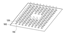
도 2는 본 발명에 의한 도전 와이어에 고경도 실리콘이 코팅되는 테스트 소켓의 부분 절개 사시도.
도 3 내지 도 6은 도 1의 제조 방법을 나타내는 사시도들.
110: 제1PCB 필름 120: 도전 와이어
122: 관통 홀 130: 절연 실리콘 고무
132: 제2패드 140: 제2PCB 필름
Claims (8)
- 다수 제1패드가 형성되는 제1PCB 필름;
상기 제1패드에 연결되는 도전 와이어;
상기 제1PCB 필름 상에 설치되고, 상기 도전 와이어에 대응되는 다수의 관통 홀이 형성되며, 상기 관통 홀에 상기 도전 와이어가 탑재되는 절연 실리콘 고무; 및
상기 절연 실리콘 고무 상에 설치되고, 제2패드를 통해 상기 도전 와이어와 연결되는 제2PCB 필름을 포함하여 구성됨을 특징으로 하는 테스트 소켓. - 제 1 항에 있어서,
상기 관통 홀은 상기 도전 와이어와 상기 절연 실리콘 고무를 상호 이격시켜 상기 도전 와이어에 대한 상기 절연 실리콘 고무의 간섭을 배제하는 것을 특징으로 하는 테스트 소켓. - 제 2 항에 있어서,
상기 도전 와이어의 외주면에는 상기 절연 실리콘 고무보다 경도가 높은 고경도 실리콘 고무가 코팅되는 것을 특징으로 하는 테스트 소켓. - 관통 홀을 포함하는 절연 실리콘 고무를 준비하는 단계;
제1PCB 필름을 준비하는 단계;
상기 제1PCB 필름 상에 도전 와이어를 연결하는 단계;
상기 제1PCB 필름 상에 절연 실리콘 고무를 설치하되, 상기 도전 와이어는 다수의 상기 관통 홀에 간섭 없이 탑재되는 단계; 및
상기 절연 실리콘 고무 상면에 제2PCB 필름이 설치되는 단계를 포함하여 구성됨을 특징으로 하는 테스트 소켓의 제조 방법. - 제 4 항에 있어서,
상기 도전 와이어를 연결한 후, 상기 도전 와이어에 고경도 실리콘 고무가 더 코팅되는 것을 특징으로 하는 테스트 소켓의 제조 방법. - 제 4 항에 있어서,
상기 도전 와이어는 상기 제1PCB 필름의 제1패드와 와이어 본딩 접합되고, 상기 제2PCB 필름의 제2패드와 도전 접착제 혹은 솔더링 접합부에 의하여 접합되는 것을 특징으로 하는 테스트 소켓의 제조 방법. - 제 4 항에 있어서,
상기 절연 실리콘 고무는 금형을 이용하여 소정 형상으로 패턴닝되고, 상기 금형에는 일정한 간격과 사이즈로 핀이 형성되며, 액상 실리콘 고무의 주입 시 상기 핀을 제외한 부분에 주입되어 상기 관통 홀이 형성되는 것을 특징으로 하는 테스트 소켓의 제조 방법. - 제 7 항에 있어서,
상기 절연 실리콘 고무는 상기 도전 와이어와 대응되지 않는 관통 홀을 더 포함하고, 상기 도전 와이어와 대응되지 않는 관통 홀은 상기 제1 및 제2PCB 필름에 의하여 커버되는 유니버셜 금형인 것을 특징으로 하는 테스트 소켓의 제조 방법.
Priority Applications (1)
| Application Number | Priority Date | Filing Date | Title |
|---|---|---|---|
| KR1020150181182A KR101800812B1 (ko) | 2015-12-17 | 2015-12-17 | 실리콘 고무에 관통 홀을 포함하는 테스트 소켓, 및 그 제조 방법 |
Applications Claiming Priority (1)
| Application Number | Priority Date | Filing Date | Title |
|---|---|---|---|
| KR1020150181182A KR101800812B1 (ko) | 2015-12-17 | 2015-12-17 | 실리콘 고무에 관통 홀을 포함하는 테스트 소켓, 및 그 제조 방법 |
Publications (2)
| Publication Number | Publication Date |
|---|---|
| KR20170072696A true KR20170072696A (ko) | 2017-06-27 |
| KR101800812B1 KR101800812B1 (ko) | 2017-11-27 |
Family
ID=59514833
Family Applications (1)
| Application Number | Title | Priority Date | Filing Date |
|---|---|---|---|
| KR1020150181182A Active KR101800812B1 (ko) | 2015-12-17 | 2015-12-17 | 실리콘 고무에 관통 홀을 포함하는 테스트 소켓, 및 그 제조 방법 |
Country Status (1)
| Country | Link |
|---|---|
| KR (1) | KR101800812B1 (ko) |
Cited By (4)
| Publication number | Priority date | Publication date | Assignee | Title |
|---|---|---|---|---|
| KR101969792B1 (ko) * | 2017-10-23 | 2019-04-17 | 주식회사 오킨스전자 | 보이드를 포함하는 테스트 소켓, 및 스페이서를 이용하는 그 제조 방법 |
| KR20210042736A (ko) | 2019-10-10 | 2021-04-20 | 한국전력공사 | 전주방호커버 |
| CN113109698A (zh) * | 2021-04-13 | 2021-07-13 | 深圳市三维电路科技有限公司 | 一种多层软硬结合线路板的缺陷测试方法 |
| CN113484560A (zh) * | 2021-07-07 | 2021-10-08 | 上海泽丰半导体科技有限公司 | 一种晶圆及成品测试共用电路板及其设计方法 |
Family Cites Families (3)
| Publication number | Priority date | Publication date | Assignee | Title |
|---|---|---|---|---|
| KR200446269Y1 (ko) | 2008-02-25 | 2009-10-29 | 주식회사 아이에스시테크놀러지 | 갭부재를 가진 테스트소켓 |
| JP2013185892A (ja) * | 2012-03-07 | 2013-09-19 | Advantest Corp | ソケット、ソケットボード、電子部品試験装置 |
| KR101544844B1 (ko) * | 2014-02-28 | 2015-08-20 | 김형익 | 와이어드 러버 컨택트 및 그 제조방법 |
-
2015
- 2015-12-17 KR KR1020150181182A patent/KR101800812B1/ko active Active
Cited By (4)
| Publication number | Priority date | Publication date | Assignee | Title |
|---|---|---|---|---|
| KR101969792B1 (ko) * | 2017-10-23 | 2019-04-17 | 주식회사 오킨스전자 | 보이드를 포함하는 테스트 소켓, 및 스페이서를 이용하는 그 제조 방법 |
| KR20210042736A (ko) | 2019-10-10 | 2021-04-20 | 한국전력공사 | 전주방호커버 |
| CN113109698A (zh) * | 2021-04-13 | 2021-07-13 | 深圳市三维电路科技有限公司 | 一种多层软硬结合线路板的缺陷测试方法 |
| CN113484560A (zh) * | 2021-07-07 | 2021-10-08 | 上海泽丰半导体科技有限公司 | 一种晶圆及成品测试共用电路板及其设计方法 |
Also Published As
| Publication number | Publication date |
|---|---|
| KR101800812B1 (ko) | 2017-11-27 |
Similar Documents
| Publication | Publication Date | Title |
|---|---|---|
| KR101737047B1 (ko) | 메탈 코어 솔더 볼을 이용하는 도전 와이어 본딩 구조체 및 그 제조방법, 그리고 이를 포함하는 테스트 소켓 | |
| KR101833009B1 (ko) | 도전성 파티클이 자화된 도전 와이어에 의하여 자성 배열되는 테스트 소켓 및 그 제조 방법 | |
| JP2016035441A (ja) | 弾性体sコンタクタを有する半導体デバイステスト用ソケット | |
| KR101800812B1 (ko) | 실리콘 고무에 관통 홀을 포함하는 테스트 소켓, 및 그 제조 방법 | |
| KR20170078457A (ko) | 와이어 실리콘 고무가 콘택 핀과 반도체 기기 사이에 인터포저 되는 번인 테스트 소켓 | |
| KR101921931B1 (ko) | 오픈 셀 구조의 fpcb 필름, 이를 포함하는 테스트 소켓, 및 그 제조 방법 | |
| KR101683017B1 (ko) | 테스트 소켓, 및 그 제조 방법 그리고 금형 | |
| KR101708487B1 (ko) | 도전 실리콘 고무 안에 더블 도전 와이어를 포함하는 테스트 소켓, 및 그 제조 방법 | |
| KR101683016B1 (ko) | 테스트 소켓, 및 그 제조 방법 | |
| KR101747385B1 (ko) | 마이크로 범프 실리콘 시트, 및 이를 포함하는 테스트 소켓 | |
| KR101311752B1 (ko) | 반도체 테스트용 콘텍터 및 그 제조방법 | |
| KR101735516B1 (ko) | 러버 범프를 포함하는 테스트 소켓 및 그 제조 방법 | |
| KR101556216B1 (ko) | 반도체 테스트 소켓 및 그 제조방법 | |
| KR101735521B1 (ko) | 스터드 범프를 포함하는 테스트 소켓 및 그 제조 방법 | |
| KR101726399B1 (ko) | 바텀 메탈 플레이트 범프를 포함하는 테스트 소켓 및 그 제조 방법 | |
| KR101802426B1 (ko) | 와이어 실리콘 보드에 의하여 mems 필름의 콘택 특성이 개선되는 하이브리드 테스트 소켓 | |
| CN112291948B (zh) | 聚硅氧烷接触元件 | |
| KR20160124347A (ko) | 고주파 디바이스 테스트용 양방향 도전성 소켓, 고주파 디바이스 테스트용 양방향 도전성 모듈 및 이의 제조방법 | |
| KR101882758B1 (ko) | 더블 s 와이어 콘택 구조의 테스트 소켓 | |
| KR101763369B1 (ko) | 개별 pcb 랜드를 포함하는 테스트 소켓 | |
| KR101717676B1 (ko) | 다수 와이어 복합체를 포함하는 테스트 소켓 | |
| KR20100069133A (ko) | 반도체소자 테스트 소켓용 스프링 컨택터 | |
| KR101744015B1 (ko) | 와이어 본딩 시 솔더 볼의 높이 편차가 해소되는 테스트 소켓의 제조 방법 | |
| KR101846303B1 (ko) | 양방향 도전성 모듈, 반도체 테스트 소켓, 그리고 그 제조방법 | |
| KR20190022249A (ko) | 양방향 도전성 모듈 및 그 제조방법 |
Legal Events
| Date | Code | Title | Description |
|---|---|---|---|
| A201 | Request for examination | ||
| PA0109 | Patent application |
Patent event code: PA01091R01D Comment text: Patent Application Patent event date: 20151217 |
|
| PA0201 | Request for examination | ||
| E902 | Notification of reason for refusal | ||
| PE0902 | Notice of grounds for rejection |
Comment text: Notification of reason for refusal Patent event date: 20170403 Patent event code: PE09021S01D |
|
| PG1501 | Laying open of application | ||
| E701 | Decision to grant or registration of patent right | ||
| PE0701 | Decision of registration |
Patent event code: PE07011S01D Comment text: Decision to Grant Registration Patent event date: 20170817 |
|
| GRNT | Written decision to grant | ||
| PR0701 | Registration of establishment |
Comment text: Registration of Establishment Patent event date: 20171117 Patent event code: PR07011E01D |
|
| PR1002 | Payment of registration fee |
Payment date: 20171120 End annual number: 3 Start annual number: 1 |
|
| PG1601 | Publication of registration | ||
| PR1001 | Payment of annual fee |
Payment date: 20201007 Start annual number: 4 End annual number: 4 |
|
| PR1001 | Payment of annual fee |
Payment date: 20211117 Start annual number: 5 End annual number: 5 |
|
| PR1001 | Payment of annual fee |
Payment date: 20221107 Start annual number: 6 End annual number: 6 |
|
| PR1001 | Payment of annual fee |
Payment date: 20241105 Start annual number: 8 End annual number: 8 |