KR20170077216A - Non-magnetic package and method of manufacture - Google Patents
Non-magnetic package and method of manufacture Download PDFInfo
- Publication number
- KR20170077216A KR20170077216A KR1020177014781A KR20177014781A KR20170077216A KR 20170077216 A KR20170077216 A KR 20170077216A KR 1020177014781 A KR1020177014781 A KR 1020177014781A KR 20177014781 A KR20177014781 A KR 20177014781A KR 20170077216 A KR20170077216 A KR 20170077216A
- Authority
- KR
- South Korea
- Prior art keywords
- magnetic
- package
- cavity
- lid
- sensitive component
- Prior art date
- Legal status (The legal status is an assumption and is not a legal conclusion. Google has not performed a legal analysis and makes no representation as to the accuracy of the status listed.)
- Granted
Links
Images



Classifications
-
- H—ELECTRICITY
- H10—SEMICONDUCTOR DEVICES; ELECTRIC SOLID-STATE DEVICES NOT OTHERWISE PROVIDED FOR
- H10W—GENERIC PACKAGES, INTERCONNECTIONS, CONNECTORS OR OTHER CONSTRUCTIONAL DETAILS OF DEVICES COVERED BY CLASS H10
- H10W76/00—Containers; Fillings or auxiliary members therefor; Seals
- H10W76/60—Seals
-
- H01L23/10—
-
- B—PERFORMING OPERATIONS; TRANSPORTING
- B81—MICROSTRUCTURAL TECHNOLOGY
- B81B—MICROSTRUCTURAL DEVICES OR SYSTEMS, e.g. MICROMECHANICAL DEVICES
- B81B7/00—Microstructural systems ; Auxiliary parts of microstructural devices or systems
- B81B7/0032—Packages or encapsulation
- B81B7/0077—Other packages not provided for in groups B81B7/0035 - B81B7/0074
-
- H01L23/29—
-
- H01L23/31—
-
- H—ELECTRICITY
- H10—SEMICONDUCTOR DEVICES; ELECTRIC SOLID-STATE DEVICES NOT OTHERWISE PROVIDED FOR
- H10W—GENERIC PACKAGES, INTERCONNECTIONS, CONNECTORS OR OTHER CONSTRUCTIONAL DETAILS OF DEVICES COVERED BY CLASS H10
- H10W74/00—Encapsulations, e.g. protective coatings
- H10W74/10—Encapsulations, e.g. protective coatings characterised by their shape or disposition
-
- H—ELECTRICITY
- H10—SEMICONDUCTOR DEVICES; ELECTRIC SOLID-STATE DEVICES NOT OTHERWISE PROVIDED FOR
- H10W—GENERIC PACKAGES, INTERCONNECTIONS, CONNECTORS OR OTHER CONSTRUCTIONAL DETAILS OF DEVICES COVERED BY CLASS H10
- H10W74/00—Encapsulations, e.g. protective coatings
- H10W74/40—Encapsulations, e.g. protective coatings characterised by their materials
-
- H01L2224/48091—
-
- H01L2224/49171—
-
- H01L2924/00014—
-
- H—ELECTRICITY
- H10—SEMICONDUCTOR DEVICES; ELECTRIC SOLID-STATE DEVICES NOT OTHERWISE PROVIDED FOR
- H10W—GENERIC PACKAGES, INTERCONNECTIONS, CONNECTORS OR OTHER CONSTRUCTIONAL DETAILS OF DEVICES COVERED BY CLASS H10
- H10W70/00—Package substrates; Interposers; Redistribution layers [RDL]
- H10W70/60—Insulating or insulated package substrates; Interposers; Redistribution layers
- H10W70/67—Insulating or insulated package substrates; Interposers; Redistribution layers characterised by their insulating layers or insulating parts
- H10W70/68—Shapes or dispositions thereof
- H10W70/682—Shapes or dispositions thereof comprising holes having chips therein
-
- H—ELECTRICITY
- H10—SEMICONDUCTOR DEVICES; ELECTRIC SOLID-STATE DEVICES NOT OTHERWISE PROVIDED FOR
- H10W—GENERIC PACKAGES, INTERCONNECTIONS, CONNECTORS OR OTHER CONSTRUCTIONAL DETAILS OF DEVICES COVERED BY CLASS H10
- H10W72/00—Interconnections or connectors in packages
- H10W72/01—Manufacture or treatment
- H10W72/013—Manufacture or treatment of die-attach connectors
- H10W72/01321—Manufacture or treatment of die-attach connectors using local deposition
- H10W72/01325—Manufacture or treatment of die-attach connectors using local deposition in solid form
-
- H—ELECTRICITY
- H10—SEMICONDUCTOR DEVICES; ELECTRIC SOLID-STATE DEVICES NOT OTHERWISE PROVIDED FOR
- H10W—GENERIC PACKAGES, INTERCONNECTIONS, CONNECTORS OR OTHER CONSTRUCTIONAL DETAILS OF DEVICES COVERED BY CLASS H10
- H10W72/00—Interconnections or connectors in packages
- H10W72/071—Connecting or disconnecting
- H10W72/073—Connecting or disconnecting of die-attach connectors
-
- H—ELECTRICITY
- H10—SEMICONDUCTOR DEVICES; ELECTRIC SOLID-STATE DEVICES NOT OTHERWISE PROVIDED FOR
- H10W—GENERIC PACKAGES, INTERCONNECTIONS, CONNECTORS OR OTHER CONSTRUCTIONAL DETAILS OF DEVICES COVERED BY CLASS H10
- H10W72/00—Interconnections or connectors in packages
- H10W72/071—Connecting or disconnecting
- H10W72/073—Connecting or disconnecting of die-attach connectors
- H10W72/07331—Connecting techniques
- H10W72/07336—Soldering or alloying
-
- H—ELECTRICITY
- H10—SEMICONDUCTOR DEVICES; ELECTRIC SOLID-STATE DEVICES NOT OTHERWISE PROVIDED FOR
- H10W—GENERIC PACKAGES, INTERCONNECTIONS, CONNECTORS OR OTHER CONSTRUCTIONAL DETAILS OF DEVICES COVERED BY CLASS H10
- H10W72/00—Interconnections or connectors in packages
- H10W72/071—Connecting or disconnecting
- H10W72/075—Connecting or disconnecting of bond wires
-
- H—ELECTRICITY
- H10—SEMICONDUCTOR DEVICES; ELECTRIC SOLID-STATE DEVICES NOT OTHERWISE PROVIDED FOR
- H10W—GENERIC PACKAGES, INTERCONNECTIONS, CONNECTORS OR OTHER CONSTRUCTIONAL DETAILS OF DEVICES COVERED BY CLASS H10
- H10W72/00—Interconnections or connectors in packages
- H10W72/071—Connecting or disconnecting
- H10W72/075—Connecting or disconnecting of bond wires
- H10W72/07531—Techniques
- H10W72/07532—Compression bonding, e.g. thermocompression bonding
- H10W72/07533—Ultrasonic bonding, e.g. thermosonic bonding
-
- H—ELECTRICITY
- H10—SEMICONDUCTOR DEVICES; ELECTRIC SOLID-STATE DEVICES NOT OTHERWISE PROVIDED FOR
- H10W—GENERIC PACKAGES, INTERCONNECTIONS, CONNECTORS OR OTHER CONSTRUCTIONAL DETAILS OF DEVICES COVERED BY CLASS H10
- H10W72/00—Interconnections or connectors in packages
- H10W72/30—Die-attach connectors
- H10W72/351—Materials of die-attach connectors
- H10W72/352—Materials of die-attach connectors comprising metals or metalloids, e.g. solders
-
- H—ELECTRICITY
- H10—SEMICONDUCTOR DEVICES; ELECTRIC SOLID-STATE DEVICES NOT OTHERWISE PROVIDED FOR
- H10W—GENERIC PACKAGES, INTERCONNECTIONS, CONNECTORS OR OTHER CONSTRUCTIONAL DETAILS OF DEVICES COVERED BY CLASS H10
- H10W72/00—Interconnections or connectors in packages
- H10W72/50—Bond wires
- H10W72/541—Dispositions of bond wires
- H10W72/5449—Dispositions of bond wires not being orthogonal to a side surface of the chip, e.g. fan-out arrangements
-
- H—ELECTRICITY
- H10—SEMICONDUCTOR DEVICES; ELECTRIC SOLID-STATE DEVICES NOT OTHERWISE PROVIDED FOR
- H10W—GENERIC PACKAGES, INTERCONNECTIONS, CONNECTORS OR OTHER CONSTRUCTIONAL DETAILS OF DEVICES COVERED BY CLASS H10
- H10W72/00—Interconnections or connectors in packages
- H10W72/851—Dispositions of multiple connectors or interconnections
- H10W72/874—On different surfaces
- H10W72/884—Die-attach connectors and bond wires
-
- H—ELECTRICITY
- H10—SEMICONDUCTOR DEVICES; ELECTRIC SOLID-STATE DEVICES NOT OTHERWISE PROVIDED FOR
- H10W—GENERIC PACKAGES, INTERCONNECTIONS, CONNECTORS OR OTHER CONSTRUCTIONAL DETAILS OF DEVICES COVERED BY CLASS H10
- H10W72/00—Interconnections or connectors in packages
- H10W72/90—Bond pads, in general
- H10W72/951—Materials of bond pads
- H10W72/952—Materials of bond pads comprising metals or metalloids, e.g. PbSn, Ag or Cu
-
- H—ELECTRICITY
- H10—SEMICONDUCTOR DEVICES; ELECTRIC SOLID-STATE DEVICES NOT OTHERWISE PROVIDED FOR
- H10W—GENERIC PACKAGES, INTERCONNECTIONS, CONNECTORS OR OTHER CONSTRUCTIONAL DETAILS OF DEVICES COVERED BY CLASS H10
- H10W76/00—Containers; Fillings or auxiliary members therefor; Seals
- H10W76/60—Seals
- H10W76/67—Seals characterised by their materials
-
- H—ELECTRICITY
- H10—SEMICONDUCTOR DEVICES; ELECTRIC SOLID-STATE DEVICES NOT OTHERWISE PROVIDED FOR
- H10W—GENERIC PACKAGES, INTERCONNECTIONS, CONNECTORS OR OTHER CONSTRUCTIONAL DETAILS OF DEVICES COVERED BY CLASS H10
- H10W90/00—Package configurations
- H10W90/701—Package configurations characterised by the relative positions of pads or connectors relative to package parts
- H10W90/731—Package configurations characterised by the relative positions of pads or connectors relative to package parts of die-attach connectors
- H10W90/734—Package configurations characterised by the relative positions of pads or connectors relative to package parts of die-attach connectors between a chip and a stacked insulating package substrate, interposer or RDL
-
- H—ELECTRICITY
- H10—SEMICONDUCTOR DEVICES; ELECTRIC SOLID-STATE DEVICES NOT OTHERWISE PROVIDED FOR
- H10W—GENERIC PACKAGES, INTERCONNECTIONS, CONNECTORS OR OTHER CONSTRUCTIONAL DETAILS OF DEVICES COVERED BY CLASS H10
- H10W90/00—Package configurations
- H10W90/701—Package configurations characterised by the relative positions of pads or connectors relative to package parts
- H10W90/751—Package configurations characterised by the relative positions of pads or connectors relative to package parts of bond wires
- H10W90/754—Package configurations characterised by the relative positions of pads or connectors relative to package parts of bond wires between a chip and a stacked insulating package substrate, interposer or RDL
Landscapes
- Engineering & Computer Science (AREA)
- Microelectronics & Electronic Packaging (AREA)
- Computer Hardware Design (AREA)
- Micromachines (AREA)
- Die Bonding (AREA)
- Physics & Mathematics (AREA)
- Health & Medical Sciences (AREA)
- Electromagnetism (AREA)
- Toxicology (AREA)
Abstract
비자성 밀봉 패키지는, 개방된 캐비티를 둘러싸는 벽 ― 벽의 상부 에지 둘레에, 일반적으로 평면인 비자성의 금속성 시일 링이 연속 루프로 배치됨 ― ; 캐비티 내에 결합되는 민감한 컴포넌트; 및 금속성 시일에 의해 캐비티를 폐쇄하기 위해 시일 링에 실링되는 비자성 덮개를 포함한다.The non-magnetic sealing package comprising: a non-magnetic metallic seal ring disposed in a continuous loop, generally planar, around the upper edge of the wall-wall surrounding the open cavity; A sensitive component coupled into the cavity; And a non-magnetic lid that is sealed to the seal ring to close the cavity by a metallic seal.
Description
본 출원은 2014년 10월 31일자로 출원된 미국 특허 출원 제14/529,311호에 대한 우선권을 주장하는데, 상기 출원의 전체는 참조에 의해 본원에 통합된다.This application claims priority to U.S. Patent Application No. 14 / 529,311, filed October 31, 2014, the entirety of which is incorporated herein by reference.
본 발명의 실시예는, 일반적으로, 온도, 습도, 및/또는 대기 성분에 민감한 디바이스의 패키징에 관한 것이다. 특정한 실시예는, 자기 공진 이미징(magnetic-resonance imaging; "MRI") 기기에서 그리고 비자성 컴포넌트를 필요로 하는 다른 애플리케이션에서 사용하기에 적합한 마이크로 전기기계 시스템(micro-electrical-mechanical systems; "MEMS")에 대한 패키지에 관한 것이다.Embodiments of the present invention generally relate to packaging devices that are sensitive to temperature, humidity, and / or ambient components. Certain embodiments include micro-electrical-mechanical systems ("MEMS") devices suitable for use in magnetic resonance imaging ("MRI") devices and in other applications requiring non- ). ≪ / RTI >
마이크로 전기기계 시스템("MEMS")은, 약 20 마이크로미터로부터 약 1 밀리미터(0.02-1.0 mm)까지의 범위 내에서 자신의 최대 치수를 갖는 디바이스이다. 이들 아주 작은 전기 기계는 예를 들면 다음과 같은 많은 애플리케이션에서 유용하다: 잉크젯 프린터의 카트리지로부터 잉크를 토출하여 페이지 상으로 글자를 쓰는 것; 셀룰러 폰 또는 게임 컨트롤러와 같은 핸드헬드 디바이스의 또는 차량의 가속도를 측정하는 것; 음압 파장 또는 표면 진동을 변환하여 사운드를 기록하는 것; 광섬유 어레이 사이에서 광학 신호를 스위칭하는 것; 등등.Microelectromechanical systems ("MEMS") are devices with their largest dimension in the range of about 20 micrometers to about 1 millimeter (0.02-1.0 mm). These very small electrical machines are useful, for example, in many applications such as: writing ink on a page by ejecting ink from a cartridge of an inkjet printer; Measuring the acceleration of a handheld device, such as a cellular phone or a game controller, or of a vehicle; Converting a sound pressure wave or surface vibration to record sound; Switching optical signals between optical fiber arrays; etc.
일반적으로, MEMS는, 작은 풋프린트 또는 볼륨 엔벨롭 내에서, 모션 감지와 같은, 고도로 응답성이 있는(작은 시간 상수의) 전기 기계 기능성을 신뢰성 있게 제공하는 데 유용하다. 따라서, MRI 시스템 내에서 감지 및 제어를 위해 MEMS를 사용하는 것이 수년 동안 소망되어 왔다. 그러나, MRI 시스템에서는, "비자성"인, 즉, 강자성(ferromagnetic)도 아니고 상자성(paramagnetic)도 아닌 컴포넌트를 제공하는 것이 필요하다.In general, MEMS is useful for reliably providing highly responsive (small time constant) electromechanical functionality, such as motion sensing, within a small footprint or volume envelope. Thus, the use of MEMS for sensing and control within an MRI system has been desired for many years. However, in an MRI system, it is necessary to provide a component that is "non-magnetic ", i.e., not ferromagnetic or paramagnetic.
현재까지, MEMS 패키징은, 강자성이거나 및/또는 상자성인 재료에 의존해 왔다. 이것은, 비자성의 재료, 예를 들면, 세라믹 또는 플라스틱으로부터 제조되는 패키지가, 패키지 내에 둘러싸이는(enclosed) MEMS에 대해 열 손상(예를 들면, 납땜(brazing)), 및/또는 화학적 손상(예를 들면, 휘발성 또는 침습성 결합제(moisture-permeable adhesive))을 주는 폐쇄 방법을 필요로 하는 것으로 이해되어 왔기 때문에, 부분적으로 이런 경우가 있어 왔다. MEMS는 그들의 환경, 미립자(particulate)에 민감하거나 또는 화학적으로 민감하고, 또한 패키징 프로세싱 조건에 민감하며, 따라서, 조건 및 패키지 환경을 제어하는 프로세스에 대한 필요성이 존재한다. 실제, MEMS는, 패키징에서 특수한 주의를 필요로 하는 "민감한" 컴포넌트의 카테고리를 대표한다. 이 카테고리의 다른 구성 요소는, 압전, 상자성, 및 형상 기억 합금 디바이스를 포함할 수도 있다.To date, MEMS packaging has relied on materials that are ferromagnetic and / or boxlike. This means that a package made from a non-magnetic material, e.g., ceramic or plastic, can be thermally damaged (e.g., brazing) and / or chemically damaged This has been the case, in part, because it has been understood to require a closure method that provides a moisture-permeable adhesive (e.g., a moisture-permeable adhesive). MEMS are sensitive to their environment, particulate, or chemically sensitive, and are also sensitive to packaging processing conditions, and therefore a need exists for processes that control conditions and package environments. In practice, MEMS represents a category of "sensitive" components that require special attention in packaging. Other components of this category may include piezoelectric, paramagnetic, and shape memory alloy devices.
상기의 관점에서, 비자성 밀봉 패키지(non-magnetic hermetic package) 내에 민감한 컴포넌트를 제공하는 것이 바람직하다. 이러한 패키지를 제공함에 있어서 주된 어려움은, 민감한 컴포넌트에 열적 및/또는 화학적 손상을 야기하지 않으면서, 민감한 컴포넌트를 개방된 비자성 패키지 캐비티 안으로 결합시키고, 그 다음, 패키지 캐비티를 실링하는(sealing) 방법을 발명하는 것이었다.In view of the above, it is desirable to provide a sensitive component in a non-magnetic hermetic package. A major difficulty in providing such a package is the method of sealing sensitive components into an open non-magnetic package cavity and then sealing the package cavity without causing thermal and / or chemical damage to the sensitive component Was invented.
본 발명의 실시예는 비자성 밀봉 MEMS 패키지를 제공하는데, 비자성 밀봉 MEMS 패키지는, 캐비티를 둘러싸는 벽을 구비하며, 일반적으로 평면인 비자성의 금속성 시일 링(seal ring)을 벽의 상부 에지 둘레에 배치한 비자성 세라믹 패키지 몸체(ceramic package body), 비자성 밀봉 MEMS 패키지; 캐비티 내에서 패키지 몸체에 결합되는 손상되지 않은 MEMS 디바이스; 및 밀봉 금속성 시일(hermetic metallic seal)에 의해 캐비티를 폐쇄하기(close) 위해, 패키지 몸체의 시일 링에 실링되는 비자성 덮개를 포함한다.An embodiment of the present invention provides a non-magnetic encapsulated MEMS package, the non-encapsulated encapsulated MEMS package having a wall enclosing the cavity and including a generally planar non-magnetic metallic seal ring around the upper edge of the wall A non-magnetic ceramic package body, a non-magnetic encapsulation MEMS package; An undamaged MEMS device coupled to the package body within the cavity; And a non-magnetic lid that is sealed to the seal of the package body to close the cavity by a hermetic metallic seal.
본 발명의 다른 실시예는 비자성 세라믹 패키지 몸체를 제공하는데, 비자성 세라믹 패키지 몸체는, 캐비티를 둘러싸는 벽; 벽의 상부 에지 둘레에 연속 루프로 배치되는 일반적으로 평면인 비자성의 금속성 시일 링; 및 캐비티 내에서 패키지 몸체에 결합되는 MEMS 디바이스를 제공한다.Another embodiment of the present invention provides a non-magnetic ceramic package body, comprising: a wall surrounding the cavity; A generally planar non-magnetic metallic seal ring disposed in a continuous loop around the upper edge of the wall; And a MEMS device coupled to the package body within the cavity.
본 발명의 다른 양태는, 개방된 캐비티를 둘러싸는 벽을 구비하는 비자성 세라믹 패키지 몸체를 형성하는 것; 패키지 몸체 벽의 상부 에지 둘레에 비자성이며 일반적으로 평면인 금속성 시일 링을 연속 루프로 설치하는 것; 캐비티 내에서 MEMS 디바이스를 패키지 몸체에 결합하는 것; 및 비자성 덮개를 시일 링에 실링하는 것을 포함하는 방법에 따라 비자성 밀봉 MEMS 패키지를 제조하는 것을 제공한다.Another aspect of the present invention is a method of forming a non-magnetic ceramic package comprising: forming a non-magnetic ceramic package body having a wall surrounding an open cavity; Mounting a non-magnetic, generally planar metallic seal ring around the upper edge of the package body wall in a continuous loop; Coupling the MEMS device to the package body within the cavity; And sealing the non-magnetic lid to the seal ring to provide a non-magnetic encapsulated MEMS package.
본 발명의 또 다른 양태는, MEMS 디바이스를 패키지 몸체에 무플럭스 솔더 결합(fluxless solder bond)하기 위한 방법을 제공하는데, 그 방법은, MEMS 디바이스의 그리고 패키지 몸체의 대향하는 면 사이에 인듐 프리폼(preform)을 제공하는 것; 플럭스 도입 없이, 리플로우 온도 범위 내에서 인듐 프리폼을 가열 및 유지하는 것; 및 인듐 프리폼을 리플로우하여 MEMS 디바이스에 그리고 패키지 몸체에 부착시키기 위해, 인듐 프리폼에 대해 MEMS 디바이스를 스크러빙(scrubbing)하는 것을 포함한다.Another aspect of the present invention provides a method for fluxless solder bonding a MEMS device to a package body, the method comprising the steps of: providing an indium preform between the opposing sides of the MEMS device and the package body; ); Heating and holding the indium preform within the reflow temperature range without flux introduction; And scrubbing the MEMS device against the indium preform to reflow the indium preform and attach it to the MEMS device and to the package body.
본 발명은, 첨부된 도면을 참조로, 비제한적인 실시예의 하기의 설명을 판독하는 것으로부터 더 잘 이해될 것인데, 이하의 도면에서:
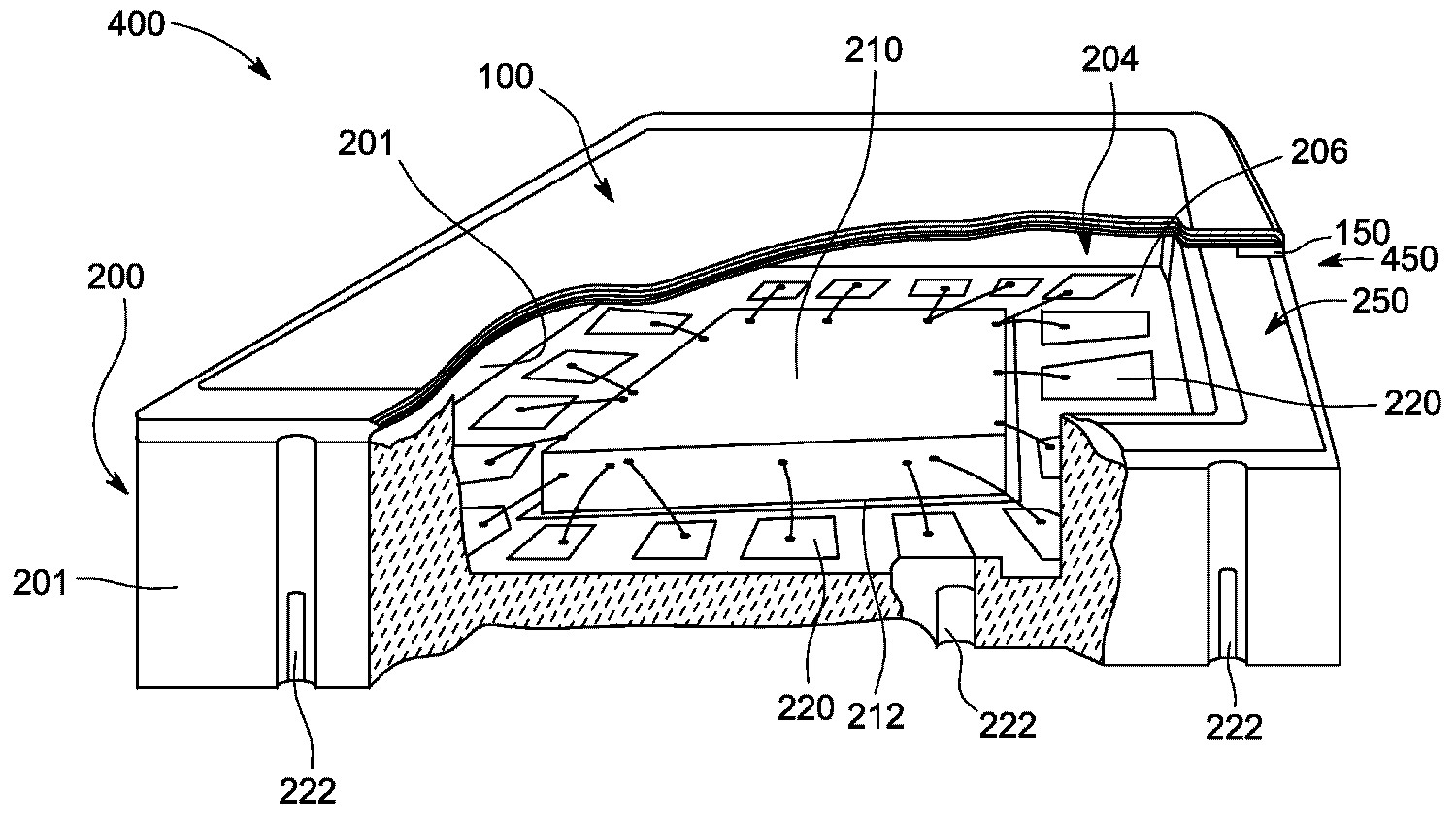
도 1은, 본 발명의 실시예에 따른, 비자성 패키지 몸체에 실링되는 예시적인 비자성 덮개를 포함하는 비자성 패키지의 부분적으로 절개된 투시도(perspective partially sectioned view)이다.
도 2는, 도 1의 비자성 덮개의 부분적으로 절개된 투시도이다.
도 3a 내지 도 3c는, 본 발명의 실시예를 제조하기 위해 사용되는 글로브 박스, 타카(tacker), 오븐, 및 심 씰러(seam sealer)의 투시도이다.
도 4는, 도 1의 비자성 덮개와 비자성 패키지 몸체 사이의 심 시일(seam-seal)의 부분적으로 절개된 상세도이다.BRIEF DESCRIPTION OF THE DRAWINGS The present invention will be better understood from reading the following description of a non-limiting embodiment, with reference to the accompanying drawings, in which:
BRIEF DESCRIPTION OF THE DRAWINGS Figure 1 is a perspective partially sectioned view of a non-magnetic package including an exemplary non-magnetic lid that is sealed to a non-magnetic package body, in accordance with an embodiment of the present invention.
Figure 2 is a partially cut away perspective view of the nonmagnetic cover of Figure 1;
Figures 3A-3C are perspective views of a glove box, a tacker, an oven, and a seam sealer used to make an embodiment of the present invention.
4 is a partially cut away detail view of a seam-seal between the non-magnetic lid of Fig. 1 and the non-magnetic package body.
하기에서는, 본 발명의 예시적인 실시예에 대한 상세한 참조가 이루어질 것인데, 본 발명의 예시적인 실시예의 예는 첨부의 도면에서 예시된다. 가능할 때마다, 도면 전체에 걸쳐 사용되는 동일한 도면 부호는, 반복적인 설명이 없는 동일한 또는 유사한 부분을 가리킨다. 비록 본 발명의 예시적인 실시예가 MRI 시스템에서의 그들의 사용과 관련하여 설명되지만, 본 발명의 실시예는, 비자성 스위치 또는 센서로부터 이익을 얻을 수 있는 임의의 설정에서의 사용을 위해 적용될 수 있다.In the following, a detailed reference will be made to an exemplary embodiment of the invention, examples of which are illustrated in the accompanying drawings. Wherever possible, the same reference numbers used throughout the drawings refer to the same or similar parts without repeating the description. Although an exemplary embodiment of the present invention is described in connection with their use in an MRI system, embodiments of the present invention may be applied for use in any configuration that may benefit from a non-magnetic switch or sensor.
본원에서 사용되는 바와 같이, 용어 "실질적으로", "일반적으로", 및 "약"은, 컴포넌트 또는 어셈블리의 기능적 목적을 달성하는 데 적합한 이상적인 소망하는 조건에 대한, 합리적으로 달성가능한 제조 및 조립 허용 오차 이내의 조건을 나타낸다.As used herein, the terms "substantially "," generally ", and "about ", when used in connection with a component or assembly, Indicates conditions within error.
예시적인 실시예에서, 도 1에서 도시되는 바와 같이, 비자성 MEMS 패키지 몸체(200)는, 일반적으로 평면인 금속성 시일 링(250)이 상부에 놓이는 벽(201)을 포함한다. 벽(201)은 캐비티(204)를 둘러싼다. 캐비티(204) 내에서는, MEMS(마이크로 전기기계) 디바이스(210)가 패키지 몸체(200) 내에서, 저온 무플럭스 인듐 솔더링 프로세스에 의해, 플로어(206)에 마운팅되는데, 플로어(206)는 다수의 레벨 또는 단(step)을 포함할 수 있다. 예시적인 "저온" 솔더링 프로세스는, 인듐 프리폼(212)을 패키지 몸체(200) 안으로 배치하는 것, 패키지 몸체를 결합 스테이지 상으로 배치하는 것, MEMS 디바이스(210)를 인듐 프리폼 상으로 배치하는 것, MEMS 디바이스 및 패키지 몸체를 약 150℃의 그러나 200℃ 이하의 리플로우 온도로 가열하는 것, 리플로우 온도에서 적어도 약 15초 동안 유지하는 것, 및 (옵션적으로, 냉각 블로우를 사용하여) 리플로우 온도로부터 냉각시키는 것을 포함한다. 통상적으로, MEMS 디바이스(210)의 하면(undersurface)("이면(backside)")뿐만 아니라 패키지 몸체 플로어(206)의 결합 영역 중 어느 하나 또는 둘 다는, TiW/Au, W/Cu/Au, 또는 W/Cu/Pd/Au와 같은 비자성의 솔더링 가능한(solderable) 코팅(도시되지 않음)으로 미리 코팅되었을 것이다.In the exemplary embodiment, as shown in FIG. 1, the non-magnetic
MEMS 구조물은, 약 200℃ 위에서 열화하거나 또는 변형하는 경향이 있는 AuNi, NiW, 또는 등등과 같은 온도에 민감한 재료 또는 합금으로부터 제조될 수 있다. 따라서, 예를 들면, 약 210℃를 초과하지 않는 결합 스테이지 헤드 온도를 갖는 저온에서의 솔더링은, MEMS 디바이스(210)에 대한 손상을 방지한다. 또한, 플럭스를 사용하지 않는 솔더링은, 플럭스 가스 배출로부터의 잠재적인 휘발성 화학약품의 소스를 제거하고, 따라서, 심 실링 이후에 MEMS 패키지(400) 내에서 화학적으로 불활성인 건조한 공기 환경이 유지되는 것을 가능하게 한다. 그러나, 산화물 및 표면 오염의 부식을 통상적으로 늦추어 솔더의 젖음성/표면 장력 및 표면 부착성을 향상시키는 플럭스를 사용하지 않으면, 산화물 불순물이 여전히 그 자리에 있는 상태에서 양호한 솔더 결합을 획득하는 것은 어려울 수 있다.MEMS structures may be fabricated from temperature sensitive materials or alloys such as AuNi, NiW, or the like which tend to degrade or deform at about 200 [deg.] C. Thus, for example, soldering at low temperatures with a combined stage head temperature that does not exceed about 210 캜 prevents damage to the
따라서, 리플로우 온도에서의 유지 동안, 플럭스 또는 불활성 대기, 즉 성형 가스(forming gas)의 사용 없이, MEMS 디바이스와 패키지 몸체(200) 사이의 양호한 기계적 결합을 달성하기 위해, 집어서 배치하는 툴(pick and place tool)이 사용되어 인듐 프리폼을 가로질러 MEMS 디바이스(210)를 스크러빙하거나 또는 왕복하고, 그에 의해 산화물을 분쇄하고 프리폼의 리플로우를 향상시킨다. MEMS 디바이스(210)의 스크러빙 모션은 순전히 횡방향의 왕복일 수도 있거나, 또는 지면의 엔벨롭(areal envelope) 내에서 또는 엄격하게는 Z 모션에서, 즉, 탭핑 모션으로서 또는 심지어 표면 장력 및 다이에 대한 솔더 산화물 층의 초기 결합을 파괴할 수도 있는 단일의 상하 모션으로서, 선회 또는 사이드 스텝식(side-stepped) 모션 또는 랜덤 모션일 수 있다. MEMS 디바이스(210)의 스크러빙 모션은 리플로우 온도 프로파일의 드웰 단계(dwell stage) 동안 달성될 수도 있다. MEMS 디바이스가 약 3 mm2인 실시예에서, MEMS 디바이스(210)에 대한 집어서 배치하는 툴의 접촉 부하는 리플로우를 달성하기 위해 적어도 약 0.2 뉴턴일 수도 있지만, MEMS 디바이스 또는 기판에 대한 설계 부하를 초과하는 것을 방지하기 위해 약 6 뉴턴 이하일 수도 있다. 소정의 실시예에서, 접촉 부하는 약 5 뉴턴일 수도 있다. 적절한 접촉 부하는 MEMS 디바이스(210)의 사이즈 및 내구성에 따라 변할 것이다. 집는 툴(pick tool)은 스크러빙 모션 내내 MEMS 디바이스(210)와 접촉하고, 집는 툴 헤드는 MEMS 디바이스를 통한 솔더로의 열 전달을 보조하도록 가열된다. 예를 들면, 집는 툴 헤드는, MEMS 디바이스에 인접한 솔더의 완전한 가열을 위해 적어도 약 150℃까지, 또는 약 180℃ 정도까지 높게 가열될 수도 있지만, MEMS 디바이스(210)에 대한 손상을 방지하기 위해 약 210℃ 이하까지 가열될 수도 있다.Thus, in order to achieve good mechanical coupling between the MEMS device and the
한 실시예에서, 시일 링(250)은 세 개의 층으로 형성된다: 텅스텐의 전이 층(252), 구리의 씨드 층(254), 및 금의 시일 층(256). 시일 링 층 재료의 각각은 인접한 층에 대한 최적의 결합을 위해 선택되는데, 예를 들면, 텅스텐 전이 층(252)은 세라믹 벽(201)에 대한 결합에 최적으로 적합되고, 한편 구리 씨드 층(254)은 텅스텐 및 금 시일 층 둘 다와 최적으로 적합된다. MEMS 디바이스(210)의 온도 제한으로 인해, 시일 링(250)은, MEMS 디바이스가 캐비티(204) 안으로 마운팅되기 이전에, 세라믹 벽(201)의 상부 에지에 형성된다. 옵션적으로, 구리와 금 사이에 팔라듐의 층의 제공될 수 있다.In one embodiment, the
일단 MEMS 디바이스(210)가, 캐비티(204)의 플로어(206)에서, 패키지 몸체(200) 상으로 기계적으로 솔더 결합되면, 그 다음, MEMS 디바이스(210)는 콘택(220)에 전기적으로 와이어본딩될 수 있는데, 콘택(220)은 캐비티(204) 내부에서부터 패키지 몸체(200)를 통해 외부 핀(222)까지 연장한다. 소정의 실시예에서, 설치된 MEMS 디바이스(210)를 통한, 외부 핀(222)의 각각의 쌍 사이의 설치시 용량(as-installed capacitance)은 약 2 pF 미만이다. 상기에서 설명되는 바와 같은 솔더 본딩 및 와이어본딩 단계에 대한 대안으로서, MEMS 디바이스(210)의 외부 금 지점(gold point)이, 대신, 패키지 몸체 상에 형성되는 금 전기 콘택(220)에 초음파로 용접될 수도 있다.Once the
와이어 본딩에 후속하여, MEMS 패키지 몸체(200), MEMS 디바이스(210), 및 덮개(100)는 (솔더 프리폼의 부착 이전에) 습기 및 다른 휘발 물질의 제거를 위해 진공 베이킹될 수도 있다. 예를 들면, 100℃/30분 드웰이 진공 오븐에서 구현될 수도 있다. 진공 베이킹 직후에, 패키지 몸체(200) 및 MEMS 디바이스(210)는 상업적으로 이용가능한 산소 애싱 프로세스(oxygen ashing process)를 사용하여 애싱될 수도 있다.Following wire bonding, the MEMS
패키지 몸체(200)의 산소 애싱 이후 약 한 시간 이내에, 그리고 통상적으로는 애싱 이후 약 30분 이내에, 덮개(100)가 (옵션적인 가고정(tacking)의 예비 단계를 가지고) 심 실링에 의해 패키지 몸체에 결합된다. 심 실링 및 가고정은 깨끗하고 "건조한 공기", 즉, 미립자가 제거된 그리고 수증기가 -40℃ 미만의 이슬점까지 또는 10,000 ppm까지 제거된 표준 공기로 채워진 글로브 박스 환경 내에서 달성된다. 예를 들면, 깨끗하고 건조한 공기는 적어도 ISO 클래스 8을; 몇몇 실시예에서는, 적어도 ISO 클래스 6을; 소정의 실시예에서는, 적어도 ISO 클래스 4를 충족하도록 필터링될 수도 있다. 상당한 분량의 산소(약 21%)를 포함하는 공기 하에서의 심 실링은, 제작시 디바이스(as-built device)에 대한 소정의 성능 목표를 달성하는 데 도움이 될 수 있다는 것을 유의해야 한다.Within about one hour after oxygen ashing of the
예를 들면, 소정의 실시예에서, MEMS 디바이스(210)의 온-저항(on-resistance)은, 초기 번인(burn-in) 이후, 1 옴(ohm) 이하로 드리프트한다. 깨끗하고 건조한 표준 공기의 밀봉 시일(hermetic seal)이, 패키지(400) 내에서, MEMS 스위치 디바이스 콘택 및 다른 표면의 평형을 이룬 산화로 귀결되기 때문에, 낮은 드리프트가 달성될 수 있다. 실링되지 않은 패키지에서 평형을 이룬 산화가 발생할 수 없다는 사실로 미루어, 그것은 또한 산소가 없는(예를 들면 불활성 가스 또는 진공의) 실링된 패키지 내에서 발생할 수 없다. 평형을 이룬 산소 층은 MEMS 스위치 콘택의 기계적 및 전기적 성능을 안정화시키도록 작용하고, 그에 의해 온-저항 드리프트를 1 옴 미만으로 유지한다.For example, in some embodiments, the on-resistance of the
계속 도 1을 참조하면, 비자성 덮개(100)(이것의 예시적 실시예는 도 2에서 더 상세히 도시된다)는 비자성 MEMS 패키지 몸체(200) 상으로 심 실링되어 밀봉된 비자성 MEMS 패키지(400)를 제공할 수 있다. 비자성 덮개(100)는, 최소한도로, 몰리브덴 기판(110) 및 덮개의 실링 표면(104)의 외주부(102) 둘레로 연장하는 금/주석 솔더 프리폼(150)을 포함한다. 도 4는, 상기에서 논의되는 바와 같이, 덮개(100)의 프리폼(150)과 패키지 몸체(200)의 시일 링(250) 사이에 형성되는 밀봉 심 시일(450)의 부분적으로 절개된 개략도를 도시한다. 본원에서 사용되는 바와 같이, "밀봉"은, 적어도 60 psi 헬륨 하에서의 두 시간 유지 이후에 헬륨 미세 누출 테스트기(helium fine leak tester)(예를 들면, Alcatel™ ASM180 모델)를 사용하여 3×10^-8 mBarr L/s 이하의 헬륨 누설율을 획득하는 것; 및 FC-40의 125C 용액에서 기포를 보이지 않는 것; 또는 등가의 테스트 결과를 의미한다.1, a non-magnetic lid 100 (an exemplary embodiment of which is shown in more detail in FIG. 2) includes a non-magnetic MEMS package (not shown) that is sealed and sealed on a non-magnetic
이제 도 3a 내지 도 3c를 참조하면, 비자성 덮개(100)는, 건조 공기 글로브 박스(310) 내에 수용되는 심 씰러(300) 및 가용접기(tack welder)(320)를 사용하는 것에 의해 비자성 MEMS 패키지 몸체(200) 상으로 실링된다. 심 씰러(300)는 자신의 전극(302)으로부터의 전류를 덮개(110)로 그리고 패키지 몸체(200)의 패턴화된 금속성 시일 링(250)으로 점진적으로 인가하고, 그에 의해 Au/Sn 프리폼을 로컬하게 리플로우하고 덮개(100)를 금속성 시일 링(250)과 함께 실링한다. 특히, 덮개(100)의 에지(102) 둘레에서의 팔라듐 층(140), 및/또는 금 코팅(160)의 결합은, 필렛(450)이 덮개의 에지를 넘어 연장하는 것을 가능하게 하고, 그에 의해 심의 실링을 향상시킨다.3A-3C, the
도 2를 특히 참조하면, 덮개(100)의 예시적인 실시예는 몰리브덴 기판(110)을 포함한다. 예를 들면, 기판(110)은 편평한 형상으로 스탬핑 또는 절단될 수도 있거나, 또는 그것은 오목한 또는 단차를 갖는(stepped) 형상으로 스탬핑 또는 묘화될 수도 있다. 기판은 적어도 약 5 밀(0.005 인치) 두께이고, 보통은 약 10 밀 두께이지만, 더 두꺼울 수 있다. 일반적으로, 기판(110)에 대한 최소 두께는, 기판의 영구적 변형 없이, 심지어 감압된 항공 화물 운송 동안에도, 패키지(400) 내에 대기압의 건조한 공기(예를 들면, 약 10,000 ppm 미만의 수증기, 또는 -40℃ 미만의 이슬점)를 유지하려는 소망에 의해 설정되며; 최대 두께는 제조의 실용성에 의해, 그리고 총 어셈블리 중량을 감소시키려는 일반적인 소망에 의해 제한된다. 몰리브덴 기판은 또한, 바람직하게는, 상기에서 설명되는 바와 같이, 로컬화된 전기적 가열에 의해 심 실링(seam-sealing)을 용이하게 할 열적 및 전기적 벌크 저항(bulk resistivity)을 제공한다.With particular reference to FIG. 2, an exemplary embodiment of
덮개(100)의 예시적인 실시예는 또한, 몰리브덴 기판(110) 위에, 적어도 약 500 옹스트롬 두께이며 약 2000 옹스트롬 두께까지 될 수 있는 결합제 층(120)을 포함한다. 결합제 층은, 티타늄으로부터 또는 탄탈 또는 크롬과 같은 유사한 몰리브덴 호환 금속으로부터 기판(110) 상으로 스퍼터링될 수 있다. 소정의 실시예에서, 스퍼터링 대신 물리적 증착(physical vapor deposition; PVD)의 등가의 방법이 사용될 수 있다. PVD 프로세스는, 음극 아크(cathodic arc), 전자 빔, 저항 증발, 펄스화된 레이저, 및 자기 스퍼터링 퇴적 기술을 포함한다. 소정의 실시예에서, 자기 스퍼터링은, 주로 전기 도금 또는 화학적 증착(chemical vapor deposition; CVD)에서의 화학적 어려움에 기인한, 코팅 방법이다. 스퍼터링된 결합제 층은, 도금된 또는 CVD 결합제 층보다 더 균일한 것으로 판명되었고 더 나은 부착성을 제공하며, 스퍼터 시스템은 부착성을 더 향상시키기 위해 백 스퍼터 성능(back sputter capability)을 제공한다. 다른 PVD 기술은, 전기화학 또는 CVD 기술과 비교하여 동등하게 적합한 것으로 여겨진다. 결합제 층(120)은 기판의 대향하는 넓은 표면 상으로 스퍼터링되고, 적어도, 스퍼터링된 영역의 에지가 연결되어 기판의 에지를 피복할 만큼 충분히 두껍고; 따라서, 결합제 층의 최소로 수용가능한 두께는 기판의 두께에 따라 변할 것이다. 결합제 층(120)은, 일반적으로, 두 개의 넓은 표면으로부터 기판의 에지를 피복하는 데 필요로 되는 것보다 훨씬 더 두껍지는 않다.An exemplary embodiment of the
결합제 층(120) 위에서, 덮개는, 적어도 약 1000 옹스트롬 두께로 스퍼터링되는 구리 씨드 층(130)을 갖는다. 구리는, 티타늄/탄탈/크롬 결합제 층과의 그것의 호환성의 관점에서, 그리고 팔라듐 전기 도금에 대한 그것의 수용성의 관점에서, 씨드 층(130)에 적합한 것으로 판명되었다. 결합제 층(120)이 기판(110)에 대한 씨드 층(130)의 부착을 크게 향상시키는 것으로 판명되었기 때문에, 씨드 층(130)은 몰리브덴 상으로 직접적으로 스퍼터링되지 않는다. 몇몇 실시예에서, 씨드 층(130)은 약 2000 옹스트롬 두께이며, 소정의 실시예에서 씨드 층은 약 6000 옹스트롬 두께만큼 두꺼울 수도 있다. 더 두꺼운 씨드 층은 전기 도금의 후속 단계로부터의 백 에칭(back-etch)을 완충하는 것을 돕고, 기판의 에지를 피복하는 것을 돕는다. 한편, 증가된 두께는 비용 및 무게를 추가하며, 고도로 열 도전성인 구리의 과도한 두께는, MEMS 패키지를 폐쇄하기 위해 덮개를 심 실링하는 후속 단계에서 문제점을 제시할 수도 있다.On the
씨드 층(130) 외부에서, 덮개(100)는, 약 1-2 ㎛ 두께인 팔라듐 솔더 베이스 층(140)을 포함하는데, 여기에서도 역시 두께는 기판(110)의 에지가 피복되는 것을 보장하도록 선택된다. 팔라듐 솔더 베이스 층(140)은, 통상적으로, 구리 씨드 층(130) 상으로 전기 도금된다. 따라서, 팔라듐 솔더 베이스 층(140)은, 구리 씨드 층의 변색(tarnishing)을 완화하도록 덮개(100)의 전체 표면을 피복할 것이다. 다른 실시예에서, 솔더 베이스 층(140)은 덮개(100)의 단지 하나의 표면(실링 표면(104)) 상으로 스퍼터링될 수도 있다.Outside of the
그 다음, 덮개(100)의 그 에지 근처의 실링 표면(104) 상에서, 금/주석 솔더 프리폼(150)이, 예를 들면, 가용접에 의해 솔더 베이스 층(140)에 부착된다. 전체적으로, 덮개(100)의 재료 및 다양한 층 두께는, 덮개 그 자체를 용접하는 것과는 대조적으로, 솔더 프리폼(150)의 스팟 심 실링을 위한 전류를 집중시키기에 충분히 높은 벌크 저항을 덮개가 가지도록 선택된다. 따라서, 본 발명의 덮개(100)는, 덮개의 또는 덮개가 부착되는 구조물의 벌크 가열(bulk heating)을 부과하지 않는 저전력 심 실링 프로세스를 허용한다. 따라서, 패키지 내의 MEMS 디바이스에 열 손상을 줄 위험성 없이, MEMS 패키지의 밀봉 실링에 대해 덮개를 사용하는 것이 가능하다. 덮개(100)는 또한, 팔라듐 솔더 베이스 층(140)과 솔더 프리폼(150) 사이에 금 플래시 층(160)을 포함할 수도 있다.A gold /
도 3을 다시 참조하면, 가고정 및 심 실링의 단계는, 건조한 조건(약 -40℃ 미만의 이슬점, 0% 상대 습도, 약 10,000 ppm 미만의 수증기) 하에서 깨끗한 공기를 유지하는 글로브 박스(310) 내에서 달성된다. 가고정 동안, 덮개(100)는 패키지 몸체(200) 상으로 배치되고 두 개의 컴포넌트가 글로브 박스 내의 가용접기(320) 안으로 함께 배치된다. 가용접기(320)는 덮개(100)를 아래로 약하게 누르기 위해 그리고 금/주석 솔더 프리폼(150)을 갖는 덮개를 하나 또는 두 위치에서 금속성 시일 링(250) 상으로 가고정하기 위해 사용된다. 가고정 이전에, 덮개(100) 및 패키지 몸체(200)는 O2 애싱/세정될 수도 있고 그 다음 CDA(하기에서 논의되는 바와 같은 깨끗하고 건조한 공기(clean dry air))로 퍼징되고(purged) 진공 오븐(330)에서 가열되는데, 진공 오븐(330)은 글로브 박스(310)와 연결되고 글로브(310) 안으로 개방되어 있다. 심 실링을 위해, 패키지 몸체(200)는 글로브 박스 내에서 심 씰러(300)의 회전가능한 스테이지(304) 상으로 이송된다.3, the steps of temporary fixing and simulated sealing are performed in a
그 다음, 심 씰러(300)는, 프리폼(150) 및 시일 링(250)이 점진적으로 로컬하게 가열되고 용접되어 솔더 베이스 층과 반대쪽 시일 링 사이에 밀봉 용접 또는 솔더 필렛을 형성하도록 덮개(100)의 에지(102)를 따라 전극 콘택을 이동시키기 위해, 전극(302)을 수축 및 연장시키면서, 덮개 및 몸체와 함께 스테이지(304)를 회전시키도록 동작된다. 이와 관련하여, 도 4에서 도시되는 바와 같이, 균일한 필렛(450)을 형성하기 위해, 기판(110)의 에지가 솔더 베이스 층(140)과 종속 층(subordinate layer)(120, 130)에 의해 완전히 피복되게 하는 것이 도움이 된다. 추가적으로, 덮개 및 패키지 몸체를, 전극(302)이 심 실링 프로세스를 시작할 단지 하나의 위치에서 함께 가고정되게 하는 것이 도움이 된다.The
본 발명의 한 양태에 따르면, 납땜(이것은 솔더 프리폼을 실링하는 것으로 잘 알려져 있음)과는 대조적으로, 로컬화된 저항 용접/가열 프로세스인 심 실링이 사용 가능하다. 비록 본 발명의 패키지(400)와 같은 패키지를 밀봉하기 위해서는 납땜 및 노(furnace) 솔더 리플로우가 통상적이었지만, 납땜 동안 획득되는 일반화된 고온은, 밀봉 MEMS 패키지 내에 둘러싸일 것으로 의도된 MEMS 디바이스를 손상 및 변형시킬 수 있다는 것이 밝혀졌다. 또한, 노에서, CDA 환경을 확립하는 것은 어렵다. 노는, 통상적으로, 대류 가열(convective heating)을 위한 성형 가스 또는 불활성 대기를 가지며, 글로브 박스 및 심 실링은 대류 가열에 대한 필요성을 제거하고 그에 의해 깨끗하고 건조한 공기의 사용을 가능하게 한다. 그러나, 심 실링을 구현하기 위해서는, 덮개(100)는 로컬화된 가열을 저항적으로 가능하게 해야 한다. 많은 비자성 금속은, 로컬 영역에서만 열을 제공하는 것을 아주 어렵게 만드는데, 그 이유는 이러한 금속이 열적으로 및/또는 전기적으로 도전성이 높은 경향이 있기 때문이다. 따라서, 덮개(100)의 재료 및 층 두께는, 이전에 고려되지 않은 방식으로 심 실링을 최적화하기 위해, 조심스럽게 선택된다.According to one aspect of the present invention, in contrast to soldering (which is well known for sealing solder preforms), simulated sealing, a localized resistance welding / heating process, is available. Although soldering and furnace solder reflow were common to seal a package such as the
상기에서 설명되는 바와 같은 프로세스는, MRI 엔클로저를 포함하는 다양한 애플리케이션에서 사용 가능한 밀봉의 그리고 비자성의 MEMS 패키지(400)로 귀결된다. 대기압의 건조한 공기가 패키지(400) 내부에서 포착되기 때문에, 그것은 또한 MEMS가 이전에는 고려되지 않았던 다른 환경에서 사용 가능할 수도 있다.The process as described above results in a sealed and
본 발명의 실시예는 비자성 밀봉 패키지를 제공하는데, 비자성 밀봉 패키지는, 내부 캐비티를 정의하는 벽 - 벽의 상부 에지 둘레에, 일반적으로 평면인 비자성의 금속성 시일 링이 배치됨 - ; 내부로부터 벽을 통해 외부 핀까지 연장하는 내부 캐비티의 적어도 하나의 전기 콘택; 캐비티 내에서 패키지 몸체에 결합되는 손상되지 않은 민감한 컴포넌트; 및 밀봉 금속성 실에 의해 캐비티를 폐쇄하기 위해 패키지 몸체의 시일 링에 실링되는 비자성 덮개를 포함한다. 시일 링은, 패키지 몸체 벽에 결합되는 텅스텐 층, 텅스텐 층 위의 구리 층, 및 구리 층 위의 금 층을 포함하는데, 금 층은 금속성 시일에 결합된다. 대안적으로, 시일 링은 W/Cu/Pd/Au 층을 포함할 수 있다. 금속성 시일은 금/주석 솔더에 의해 형성될 수도 있다. 예를 들면, 금속성 시일은, 금/주석 솔더를, 금속성 시일 링의 금 층에 심 실링하는 것에 의해 형성될 수도 있다. 따라서, 비자성 덮개는, 덮개의 실링 표면에서, 금/주석 솔더 프리폼을 포함할 수도 있다. 패키지는 또한, 민감한 컴포넌트와 전기적으로 연결되는, 캐비티 내부의 전기적 콘택을 포함할 수도 있고, 패키지 벽 상에 형성되며 캐비티 내부의 전기적 콘택 및 민감한 컴포넌트를 통해 서로 전기적으로 연결되는 외부 핀을 더 포함할 수도 있는데, 민감한 컴포넌트를 통한 외부 핀 사이의 캐패시턴스는 약 2 pF 미만이다. 민감한 컴포넌트는 MEMS 디바이스일 수도 있으며, 특히 번인 이후에 1 옴 미만으로 드리프트하는 안정된 온-저항, 및/또는 적어도 약 250 V의 차단 전압(blocking voltage)을 갖는 스위치일 수도 있다. 비자성 덮개는, 대략적으로 대기 산소 농도를 갖는 깨끗하고 건조한 공기에서 시일 링에 심 실링될 수도 있다.An embodiment of the present invention provides a non-magnetic encapsulation package, wherein a non-magnetic metallic seal ring, which is generally planar, is disposed around the upper edge of the wall-wall defining the inner cavity; At least one electrical contact of the inner cavity extending from the interior to the exterior pin through the wall; An undamaged sensitive component coupled to the package body within the cavity; And a non-magnetic lid that is sealed to the seal ring of the package body for closing the cavity by the sealed metallic seal. The seal ring includes a tungsten layer coupled to the package body wall, a copper layer over the tungsten layer, and a gold layer over the copper layer, wherein the gold layer is bonded to the metallic seal. Alternatively, the seal ring may comprise a W / Cu / Pd / Au layer. The metallic seal may be formed by gold / tin solder. For example, the metallic seal may be formed by simul- tively sealing the gold / tin solder to the gold layer of the metallic seal ring. Thus, the nonmagnetic lid may comprise a gold / tin solder preform on the sealing surface of the lid. The package may also include an electrical contact inside the cavity, electrically connected to the sensitive component, and further comprising an outer pin formed on the package wall and electrically connected to the electrical contact and the sensitive component within the cavity The capacitance between the external pin through the sensitive component is less than about 2 pF. The sensitive component may be a MEMS device, in particular a switch with stable on-resistance drifting below 1 ohm after burn-in, and / or a blocking voltage of at least about 250 volts. The nonmagnetic lid may be simul-sealed to the seal in clean, dry air with approximately atmospheric oxygen concentration.
본 발명의 다른 실시예는 비자성 세라믹 패키지를 제공하는데, 비자성 세라믹 패키지는, 캐비티를 둘러싸는 벽; 벽의 상부 에지 둘레의 일반적으로 평면인 비자성의 금속성 시일 링; 및 내부로부터 벽을 통해 외부 핀까지 연장하는 내부 캐비티 내의 적어도 하나의 전기적 콘택을 포함한다. 시일 링은, 패키지 몸체 벽에 결합된 텅스텐 층, 텅스텐 층 위의 구리 층, 및 구리 층 위의 금 층을 포함한다. 시일 링은 또한, 금 층과 구리 층 사이에 팔라듐 층을 포함할 수도 있다. 민감한 컴포넌트는, 무플럭스의 저온 솔더 프로세스를 사용하여 패키지 몸체에 결합되었을 수도 있다. 솔더 프로세스에서 인듐이 사용되었을 수도 있다.Another embodiment of the present invention provides a non-magnetic ceramic package, the non-magnetic ceramic package comprising: a wall surrounding the cavity; A generally planar non-magnetic metallic seal ring around the upper edge of the wall; And at least one electrical contact in the interior cavity extending from the interior to the exterior pin through the wall. The seal ring includes a tungsten layer coupled to the package body wall, a copper layer over the tungsten layer, and a gold layer over the copper layer. The seal ring may also include a palladium layer between the gold layer and the copper layer. Sensitive components may be coupled to the package body using a fluxless low temperature solder process. Indium may have been used in the solder process.
본 발명의 다른 양태는, 개방된 캐비티를 둘러싸는 벽을 구비하는 그리고 패키지 몸체 벽의 상부 에지 둘레에 비자성이며 일반적으로 평면인 금속성 시일 링을 연속 루프로 구비하는 비자성 세라믹 패키지 몸체를 형성하는 것; 캐비티 내에서 패키지 몸체에 민감한 컴포넌트를 결합하는 것; 및 비자성 덮개를 시일 링에 실링하는 것을 포함하는 방법에 따라 비자성 밀봉 패키지를 제조하는 것을 제공한다. 시일 링을 설치하는 것은, 패키지 몸체 벽에 결합될 텅스텐 층을 먼저 형성하는 것에 의해 비자성이며 일반적으로 평면인 금속성 시일 링은 형성하는 것, 그 다음 구리 층을 텅스텐 층 상으로 퇴적하는 것, 및 그 다음 구리 층 위로 금 층을 퇴적하는 것을 포함할 수도 있다. 몇몇 양태에서, 시일 링을 설치하는 것은, 패키지 몸체 벽의 상부 에지 둘레에 텅스텐 층을 연속 루프로 퇴적하는 것, 그 다음 구리 층을 텅스텐 층 상으로 퇴적하는 것, 및 그 다음, 금 층을 구리 층 위로 퇴적하는 것을 포함할 수도 있다. 민감한 컴포넌트를 결합하는 것은 무플럭스의 저온 솔더 프로세스를 포함할 수도 있는데, 무플럭스의 저온 솔더 프로세스에서는 인듐이 저온 솔더로서 사용될 수도 있다. 저온 솔더 프로세스는, 패키지 몸체와 관련한, 민감한 컴포넌트의 스크러빙 모션을 포함할 수도 있다. 방법의 소정의 양태는, 민감한 컴포넌트의 그리고 패키지 몸체 캐비티의 대향하는 면을, 본질적으로 TiW/Au 또는 W/Cu/Au로 구성되는 비자성의 솔더링 가능한 코팅으로 미리 코팅하는 것을 포함할 수도 있다. 비자성 덮개를 실링하는 것은, 심 실링 프로세스로서 실행될 수도 있다. 옵션적으로, 패키지 몸체 및 민감한 컴포넌트는, 비자성 덮개를 비자성의 금속성 시일 링에 실링하기 이전에 애싱될 수도 있고 및/또는 진공 베이킹될 수도 있다. 옵션적으로, 비자성 덮개를 심 실링하는 것은 약 1 atm의 건조한 공기 하에서 달성될 수도 있다. 추가적으로, 패키지 몸체, 민감한 컴포넌트, 및 덮개는, 비자성 덮개를 비자성의 금속성 시일 링에 실링하기 이전에, 오븐에서 약 1atm의 건조한 공기 하에서 가열될 수도 있다.Another aspect of the invention is a method of forming a non-magnetic ceramic package body having a wall surrounding an open cavity and comprising a metallic seal ring in a continuous loop that is non-magnetic and generally planar about an upper edge of the package body wall that; Combining sensitive components in the package body within the cavity; And sealing the non-magnetic lid to the seal ring to produce a non-magnetic encapsulation package. Providing the seal ring can be accomplished by first forming a tungsten layer to be bonded to the package body wall, thereby forming a metallic seal that is non-magnetic and generally planar, then depositing the copper layer onto the tungsten layer, and And then depositing a gold layer over the copper layer. In some aspects, installing the seal ring may include depositing a tungsten layer in a continuous loop around the upper edge of the package body wall, then depositing the copper layer onto the tungsten layer, Depositing on top of the layer. Combining sensitive components may include a fluxless low-temperature solder process, where indium may be used as a low-temperature solder in a fluxless low-temperature solder process. The low temperature solder process may include scrubbing motion of the sensitive component with respect to the package body. Certain aspects of the method may include precoating the opposite side of the sensitive component and the package body cavity with a nonmagnetic, solderable coating consisting essentially of TiW / Au or W / Cu / Au. Sealing the nonmagnetic lid may also be performed as a simmering process. Optionally, the package body and the sensitive component may be ashed and / or vacuum baked prior to sealing the non-magnetic lid to the non-magnetic metallic seal ring. Optionally, simmering the non-magnetic sheath may be accomplished under dry air at about 1 atm. Additionally, the package body, the sensitive component, and the cover may be heated in an oven at about 1 atm of dry air prior to sealing the non-magnetic lid to the non-magnetic metallic seal ring.
본 발명의 다른 양태는, MEMS 디바이스를 패키지 몸체에 무플럭스 솔더 결합하기 위한 방법을 제공하는데, 그 방법은, MEMS 디바이스의 그리고 패키지 몸체의 대향하는 면 사이에 인듐 프리폼을 제공하는 것; 플럭스 또는 성형 가스 도입 없이, 리플로우 온도 범위 내에서 인듐 프리폼을 가열 및 유지하는 것; 및 인듐 프리폼을 리플로우하여 MEMS 디바이스에 그리고 패키지 몸체에 부착시키기 위해, 인듐 프리폼에 대해 MEMS 디바이스를 스크러빙하는 것을 포함한다. 방법은 또한, 대향하는 면 중 적어도 하나를 비자성의 솔더링 가능한 코팅으로 미리 코팅하는 것을 포함할 수도 있다. 예를 들면, 비자성의 솔더링 가능한 코팅은 TiW/Au 또는 W/Cu/Au 중 어느 하나를 포함할 수도 있다. 리플로우 온도 범위는 약 150℃와 약 210℃ 사이에 있을 수도 있다. 예를 들면, 인듐 프리폼은 약 200℃에서 그러나 약 210℃ 이하에서 유지될 수도 있다. 인듐 프리폼은 패키지 몸체를 통해 그리고 MEMS 디바이스를 통해 가열될 수도 있다.Another aspect of the invention provides a method for fluxless solder bonding a MEMS device to a package body, the method comprising: providing an indium preform between the opposing sides of the MEMS device and the package body; Heating and holding the indium preform within the reflow temperature range without flux or molding gas introduction; And scrubbing the MEMS device against the indium preform to reflow and attach the indium preform to the MEMS device and to the package body. The method may also include precoating at least one of the opposing surfaces with a nonmagnetic, solderable coating. For example, the non-magnetic, solderable coating may comprise either TiW / Au or W / Cu / Au. The reflow temperature range may be between about 150 ° C and about 210 ° C. For example, the indium preform may be maintained at about 200 캜 but below about 210 캜. The indium preform may be heated through the package body and through the MEMS device.
상기 설명은 제한적인 것이 아니라 예시적인 것으로 의도된다는 것이 이해되어야 한다. 예를 들면, 상기 설명된 실시예(및/또는 그 양태)는 서로 조합하여 사용될 수도 있다. 또한, 본 발명의 범위를 벗어나지 않으면서 특정한 상황 또는 재료를 본 발명의 교시에 적응시키기 위해 많은 수정이 이루어질 수도 있다. 본원에서 설명되는 재료의 치수 및 타입은 본 발명의 파라미터를 정의하도록 의도되지만, 이들은 결코 제한하는 것이 아니며 예시적인 실시예가다. 상기 설명의 검토시, 많은 다른 실시예가 기술 분야의 숙련된 자에게 명백할 것이다. 따라서, 본 발명의 범위는, 첨부된 청구범위의 자격이 부여되는 등가의 완전한 범위와 함께, 첨부된 청구범위를 참조하여 결정된다. 첨부된 청구범위에서, 용어 "포함하는(including)" 및 "~는데(in which)"는 각각의 용어 "포함하는(comprising)" 및 "~는데(wherein)"의 평문 영어의 등가물로서 사용된다. 또한, 하기의 청구범위에서, "제1", "제2", "제3", "상위(upper)", "하위(lower)", "저부(bottom)", "상부(top)", 등등은 단지 라벨로서 사용되며, 그들 대상물에 수치적 또는 위치적 요건을 부과하도록 의도되지는 않는다. 또한, 하기의 청구범위의 제한사항(limitations)은, 이러한 청구범위 제한사항이 추가적인 구조물 없이 기능의 진술이 후속하는 어구 "~위한 수단"을 명시적으로 사용하지 않는 한 그리고 명시적으로 사용할 때까지, 기능식 청구항(means-plus-function) 포맷으로 작성되지 않으며 35 U.S.C. §112, 제6 패러그래프에 기초하여 해석되도록 의도되지 않는다.It is to be understood that the above description is intended to be illustrative, not limiting. For example, the above-described embodiments (and / or aspects thereof) may be used in combination with one another. In addition, many modifications may be made to adapt a particular situation or material to the teachings of the invention without departing from its scope. The dimensions and types of materials described herein are intended to define the parameters of the present invention, but they are by no means limiting and are exemplary embodiments. Many other embodiments will be apparent to those skilled in the art upon review of the above description. Accordingly, the scope of the invention is to be determined with reference to the appended claims, along with the full scope of equivalents to which such claims are entitled. In the appended claims, the terms "including" and "in which" are used as the equivalent of each word "comprising" and " . Also, in the following claims, the terms "first," "second," "third," "upper," "lower," "bottom," " , Etc. are used merely as labels and are not intended to impose numerical or positional requirements on their objects. Also, the limitations of the following claims are not to be construed as limitations of the claims until such claim restrictions are explicitly used and unless expressly used by the phrase "means for " , Is not written in a means-plus-function format, and is 35 USC It is not intended to be interpreted on the basis of §112, sixth paragraph.
이 작성된 설명은, 최상의 모드를 비롯한, 본 발명의 여러가지 실시예를 개시하기 위해, 그리고 또한 기술 분야의 숙련된 자가, 임의의 디바이스 또는 시스템을 만들고 사용하는 것 및 임의의 통합된 방법을 수행하는 것을 비롯하여, 본 발명의 실시예를 실시하는 것을 가능하게 하기 위해, 예를 사용한다. 본 발명의 특허가능한 범위는 청구범위에 의해 정의되며, 기술 분야에서 숙련된 자 중 한 명이 떠올리는 다른 예를 포함할 수도 있다. 이러한 다른 예는, 이러한 다른 예가 청구범위의 문자적 언어와는 상이하지 않은 구조적 엘리먼트를 가지면, 또는 이러한 다른 예가 청구범위의 문자적 언어와는 비실질적 차이(insubstantial difference)를 갖는 등가의 구조적 엘리먼트를 포함하면, 청구범위의 범위 내에 있는 것으로 의도된다.This written description uses examples to describe various embodiments of the present invention, including the best mode, and also to enable any person skilled in the art to make and use any device or system, and to perform any integrated method In order to enable implementation of the embodiments of the present invention, an example is used. The patentable scope of the invention is defined by the claims, and may include other examples of which one skilled in the art will recognize. Another such example is that if such another example has a structural element that is not different from the literal language of the claims, or if such other example has an equivalent structural element with an insubstantial difference from the literal language of the claims Are intended to be within the scope of the claims.
본원에서 사용되는 바와 같이, 단수형으로 언급되는 그리고 단어 "한(a)" 또는 "한(an)"으로 진행하는 엘리먼트 또는 단계는, 배제가 명시적으로 언급되지 않는 한, 상기 엘리먼트 또는 단계의 복수형을 배제하지 않는 것으로 이해되어야 한다. 또한, "하나의 실시예"에 대한 언급은, 열거된 피쳐를 또한 통합하는 추가적인 실시예의 존재를 배제하는 것으로 해석되도록 의도되지는 않는다. 또한, 명시적으로 반대로 언급되지 않는 한, 특정한 속성을 구비하는 엘리먼트 또는 복수의 엘리먼트를 "포함하는(comprising)", 포함하는(including), 또는 "구비하는(having)" 실시예는, 그 속성을 구비하지 않는 추가적인 이러한 엘리먼트를 포함할 수도 있다.As used herein, an element or step referred to in the singular and proceeding with the words "a" or " an "means that, unless an exclusion is explicitly stated, And the like. In addition, references to "one embodiment" are not intended to be construed as excluding the existence of additional embodiments that also incorporate the listed features. In addition, unless explicitly stated to the contrary, the term "comprising," "including," or "having" an element or elements having a particular attribute, And may include additional such elements without.
본원에서 수반되는 본 발명의 취지와 범위를 벗어나지 않으면서, 상기 설명된 물품 및 제조 방법에서 소정의 변경이 이루어질 수도 있기 때문에, 상기 설명의 또는 첨부의 도면에서 도시되는 주제(subject matter)의 전체는, 단지 본원의 발명적 개념을 예시하는 예로서 해석되어야 하고 본 발명을 제한하는 것으로서 간주되지 않아야 한다는 것이 의도된다.As certain changes may be made in the above described articles and manufacturing methods without departing from the spirit and scope of the invention as hereinafter claimed, all of the subject matter shown in the above description or in the accompanying drawings , It is to be construed as merely illustrative of the inventive concept of the present application and should not be construed as limiting the present invention.
Claims (29)
개방된 캐비티를 둘러싸는 벽 ― 상기 벽의 상부 에지 둘레에, 일반적으로 평면인 비자성의 금속성 시일 링(seal ring)이 연속 루프로 배치됨 ― ;
상기 캐비티 내에 결합되는(bonded) 민감한 컴포넌트(sensitive component); 및
금속성 시일에 의해 상기 캐비티를 폐쇄하기 위해 상기 시일 링에 실링되는(sealed) 비자성 덮개
를 포함하는, 비자성 밀봉 패키지.In a non-magnetic hermetic package,
A wall surrounding the open cavity - around the upper edge of the wall, a generally planar non-magnetic metallic seal ring is disposed in a continuous loop;
A sensitive component bonded within the cavity; And
A non-magnetic lid sealed to the seal ring for closing the cavity by a metallic seal,
/ RTI > The non-magnetic encapsulation package of claim <
상기 시일 링은, 패키지 몸체 벽에 결합되는 텅스텐 층, 상기 텅스텐 층 위의 구리 층, 및 상기 구리 층 위의 금 층을 포함하며, 상기 금 층은 상기 금속성 시일에 결합되는 것인, 비자성 밀봉 패키지.The method according to claim 1,
Wherein the seal ring comprises a tungsten layer coupled to the package body wall, a copper layer over the tungsten layer, and a gold layer over the copper layer, wherein the gold layer is bonded to the metallic seal. package.
상기 시일 링은, 상기 벽에 결합되는 텅스텐 층, 상기 텅스텐 층 위의 구리 층, 상기 구리 층 위의 팔라듐 층, 및 상기 금속성 시일에 결합되는 금 층을 포함하는 것인, 비자성 밀봉 패키지.The method according to claim 1,
Wherein the seal ring comprises a tungsten layer coupled to the wall, a copper layer over the tungsten layer, a palladium layer over the copper layer, and a gold layer bonded to the metallic seal.
상기 금속성 시일은 금/주석 솔더에 의해 형성되는 것인, 비자성 밀봉 패키지.The method according to claim 1,
Wherein the metallic seal is formed by a gold / tin solder.
상기 민감한 컴포넌트와 전기적으로 연결되는, 상기 캐비티 내부의 전기적 콘택을 더 포함하는, 비자성 밀봉 패키지.The method according to claim 1,
Further comprising an electrical contact within the cavity, the electrical contact electrically coupled to the sensitive component.
상기 패키지 벽 상에 형성되며 상기 캐비티 내부의 상기 전기적 콘택 및 상기 민감한 컴포넌트를 통해 서로 전기적으로 연결되는 외부 핀을 더 포함하고, 상기 민감한 컴포넌트를 통한 상기 외부 핀 사이의 캐패시턴스는 약 2 pF 미만인 것인, 비자성 밀봉 패키지.6. The method of claim 5,
Further comprising an outer pin formed on the package wall and electrically connected to each other through the electrical contact and the sensitive component within the cavity, wherein a capacitance between the outer pin through the sensitive component is less than about 2 pF , Non-magnetic sealing package.
상기 민감한 컴포넌트는 MEMS 디바이스인 것인, 비자성 밀봉 패키지.The method according to claim 1,
Wherein the sensitive component is a MEMS device.
상기 MEMS 디바이스는, 번인(burn-in) 이후 1 옴 미만으로 드리프트하는 안정된 온-저항(on-resistance)을 갖는 스위치인 것인, 비자성 밀봉 패키지.8. The method of claim 7,
Wherein the MEMS device is a switch having a stable on-resistance that drifts less than one ohm after burn-in.
상기 MEMS 디바이스는, 적어도 약 250 V의 차단 전압(blocking voltage)을 갖는 스위치인 것인, 비자성 밀봉 패키지.8. The method of claim 7,
Wherein the MEMS device is a switch having a blocking voltage of at least about 250 volts.
상기 비자성 덮개는, 대략적으로 대기 산소 농도를 갖는 깨끗하고 건조한 공기에서 상기 시일 링에 심 실링되는(seam sealed), 비자성 밀봉 패키지.The method according to claim 1,
The nonmagnetic lid is seam sealed to the seal ring in clean, dry air having an approximately atmospheric oxygen concentration.
상기 패키지는 기체 산소를 포함하는, 비자성 밀봉 패키지.The method according to claim 1,
Wherein the package comprises gaseous oxygen.
상기 패키지는 약 -40℃ 미만의 이슬점을 갖는 깨끗하고 건조한 공기를 포함하는, 비자성 밀봉 패키지.12. The method of claim 11,
Wherein the package comprises clean, dry air having a dew point of less than about -40 占 폚.
상기 덮개는 비자성인 것인, 비자성 밀봉 패키지.The method according to claim 1,
Wherein the lid is non-permeable.
상기 덮개는 금속성인 것인, 비자성 밀봉 패키지.14. The method of claim 13,
Wherein the cover is metallic.
상기 덮개는 몰리브덴을 포함하는 것인, 비자성 밀봉 패키지.15. The method of claim 14,
Wherein the lid comprises molybdenum.
내부 캐비티를 정의하는 벽;
상기 벽의 상부 에지 둘레의 일반적으로 평면인 비자성의 금속성 시일 링; 및
내부로부터 상기 벽을 통해 외부 핀까지 연장하는 상기 내부 캐비티 내의 적어도 하나의 전기적 콘택
을 포함하고,
상기 시일 링은 텅스텐 층, 구리 층, 팔라듐 층, 및 금 층을 포함하는 것인, 비자성 패키지.In a non-magnetic package,
A wall defining an internal cavity;
A generally planar non-magnetic metallic seal ring around the upper edge of said wall; And
At least one electrical contact in the inner cavity extending from the interior to the exterior pin through the wall,
/ RTI >
Wherein the seal ring comprises a tungsten layer, a copper layer, a palladium layer, and a gold layer.
무플럭스 저온 프로세스(fluxless low temperature process)를 사용하여 상기 캐비티 안으로 결합되는 민감한 컴포넌트를 더 포함하는, 비자성 패키지.17. The method of claim 16,
The non-magnetic package further comprising a sensitive component coupled into the cavity using a fluxless low temperature process.
상기 결합 프로세스에서 인듐 솔더가 사용되는 것인, 비자성 패키지.18. The method of claim 17,
Wherein indium solder is used in the bonding process.
상기 결합 프로세스는, 상기 패키지 몸체 내의 상기 민감한 컴포넌트의 스크러빙(scrubbing) 모션을 포함하는 것인, 비자성 패키지.19. The method of claim 18,
Wherein the coupling process comprises scrubbing motion of the sensitive component in the package body.
상기 결합 프로세스는 상기 적어도 하나의 전기적 콘택에 대한 상기 민감한 컴포넌트의 초음파 용접을 포함하는 것인, 비자성 패키지.18. The method of claim 17,
Wherein the bonding process comprises ultrasonic welding of the sensitive component to the at least one electrical contact.
개방된 캐비티를 둘러싸는 벽을 구비하며 상기 벽의 상부 에지 둘레에 비자성이며 일반적으로 평면인 금속성 시일 링을 연속 루프로 구비하는 비자성 세라믹 패키지 몸체를 획득하는 단계;
상기 캐비티 내에서 민감한 컴포넌트를 결합하는 단계; 및
비자성 덮개를 상기 시일 링에 실링하는 단계
를 포함하는, 비자성 밀봉 패키지를 제조하기 위한 방법.A method for manufacturing a non-magnetic encapsulation package,
Obtaining a non-magnetic ceramic package body having a wall surrounding the open cavity and having a metallic seal ring in a continuous loop that is non-magnetic and generally planar about the upper edge of the wall;
Coupling a sensitive component within the cavity; And
Sealing the non-magnetic lid to the seal ring
0.0 > a < / RTI > non-magnetic encapsulation package.
상기 민감한 컴포넌트를 결합하는 단계는 무플럭스의 저온 솔더 프로세스를 포함하는 것인, 비자성 밀봉 패키지를 제조하기 위한 방법.22. The method of claim 21,
Wherein coupling the sensitive component comprises a fluxless solder process of fluxlessness.
상기 저온 솔더로서 인듐이 사용되는 것인, 비자성 밀봉 패키지를 제조하기 위한 방법.23. The method of claim 22,
Wherein indium is used as said low temperature solder.
상기 결합 프로세스는, 상기 패키지 몸체와 관련한 상기 민감한 컴포넌트의 스크러빙 모션을 포함하는 것인, 비자성 밀봉 패키지를 제조하기 위한 방법.22. The method of claim 21,
Wherein the bonding process comprises scrubbing motion of the sensitive component with respect to the package body.
상기 비자성 덮개를 실링하는 단계는 산소 하에서 달성되는 것인, 비자성 밀봉 패키지를 제조하기 위한 방법.22. The method of claim 21,
Wherein the step of sealing the nonmagnetic lid is accomplished under oxygen.
상기 비자성 덮개를 실링하는 단계는 심 실링 프로세스인 것인, 비자성 밀봉 패키지를 제조하기 위한 방법.22. The method of claim 21,
Wherein the step of sealing the non-magnetic lid is a simulated sealing process.
상기 민감한 컴포넌트의 그리고 상기 캐비티의 대향하는 면을, 본질적으로 TiW/Au 또는 W/Cu/Au로 구성되는 비자성의 솔더링 가능한 코팅(non-magnetic solderable coating)으로 미리 코팅하는 단계를 더 포함하는, 비자성 밀봉 패키지를 제조하기 위한 방법.22. The method of claim 21,
Further comprising precoating the opposite side of the sensitive component and the cavity with a non-magnetic solderable coating consisting essentially of TiW / Au or W / Cu / Au. A method for manufacturing a hermetic seal package.
상기 비자성 덮개를 상기 비자성의 금속성 시일 링에 실링하기 이전에 상기 패키지 몸체 및 상기 민감한 컴포넌트를 애싱하고 진공 베이킹하는 단계를 더 포함하는, 비자성 밀봉 패키지를 제조하기 위한 방법.22. The method of claim 21,
Further comprising ashing and vacuum baking the package body and the sensitive component prior to sealing the non-magnetic lid to the non-magnetic metallic seal ring.
상기 MEMS 디바이스의 그리고 상기 패키지 몸체의 대향하는 면 사이에 인듐 프리폼(preform)을 제공하는 단계;
플럭스 또는 성형 가스(forming gas)를 도입하지 않으면서, 상기 인듐 프리폼을 리플로우 온도 범위 내에서 가열하고 유지하는 단계; 및
상기 인듐 프리폼을 상기 MEMS 디바이스로 그리고 상기 패키지 몸체로 리플로우하여 부착하기 위해 상기 인듐 프리폼에 대해 상기 MEMS 디바이스를 스크러빙하는 단계
를 포함하는, MEMS 디바이스를 패키지 몸체에 무플럭스 솔더 결합하기 위한 방법.A method for fluxless solder bonding a MEMS device to a package body,
Providing an indium preform between the opposing sides of the MEMS device and the package body;
Heating and maintaining the indium preform within the reflow temperature range without introducing a flux or forming gas; And
Scrubbing the MEMS device against the indium preform to reflow and attach the indium preform to the MEMS device and to the package body
Wherein the MEMS device is mounted on the package body.
Applications Claiming Priority (3)
| Application Number | Priority Date | Filing Date | Title |
|---|---|---|---|
| US14/529,311 | 2014-10-31 | ||
| US14/529,311 US10431509B2 (en) | 2014-10-31 | 2014-10-31 | Non-magnetic package and method of manufacture |
| PCT/US2015/057517 WO2016069560A1 (en) | 2014-10-31 | 2015-10-27 | Non-magnetic package and method of manufacture |
Publications (2)
| Publication Number | Publication Date |
|---|---|
| KR20170077216A true KR20170077216A (en) | 2017-07-05 |
| KR102483117B1 KR102483117B1 (en) | 2022-12-29 |
Family
ID=55853508
Family Applications (1)
| Application Number | Title | Priority Date | Filing Date |
|---|---|---|---|
| KR1020177014781A Active KR102483117B1 (en) | 2014-10-31 | 2015-10-27 | Non-magnetic package and method of manufacture |
Country Status (8)
| Country | Link |
|---|---|
| US (2) | US10431509B2 (en) |
| EP (1) | EP3213101B1 (en) |
| JP (1) | JP6629317B2 (en) |
| KR (1) | KR102483117B1 (en) |
| CN (1) | CN107004642B (en) |
| CA (1) | CA2966183C (en) |
| SG (1) | SG11201703295RA (en) |
| WO (1) | WO2016069560A1 (en) |
Families Citing this family (12)
| Publication number | Priority date | Publication date | Assignee | Title |
|---|---|---|---|---|
| US10431509B2 (en) * | 2014-10-31 | 2019-10-01 | General Electric Company | Non-magnetic package and method of manufacture |
| CN106772142A (en) * | 2016-11-25 | 2017-05-31 | 中国科学院地质与地球物理研究所 | A kind of fluxgate sensor and its manufacture method |
| US11309251B2 (en) | 2017-07-31 | 2022-04-19 | AdTech Ceramics Company | Selective metallization of integrated circuit packages |
| JP6784317B2 (en) * | 2018-10-15 | 2020-11-11 | 三菱マテリアル株式会社 | Package lid material and package manufacturing method |
| CN110112039A (en) * | 2019-05-24 | 2019-08-09 | 中汇瑞德电子(芜湖)有限公司 | A kind of sealed relay and its encapsulating method |
| US12235144B2 (en) * | 2020-09-17 | 2025-02-25 | Applied Materials, Inc.—Robotics | Micro-electromechanical device for use in a flow control apparatus |
| CN115312549A (en) * | 2021-05-05 | 2022-11-08 | 胜丽国际股份有限公司 | Sensor packaging structure |
| CN117242567A (en) * | 2021-05-12 | 2023-12-15 | 三菱电机株式会社 | Hermetically sealed components and component modules |
| JP7652160B2 (en) | 2022-09-08 | 2025-03-27 | 株式会社村田製作所 | Electronic component package and method for manufacturing the same |
| BE1031732B1 (en) * | 2023-06-22 | 2025-02-03 | C Mac Electromag Bvba | SEMICONDUCTOR COVER WITH SOLDER MATERIAL GASKET |
| WO2025034788A1 (en) * | 2023-08-10 | 2025-02-13 | Kyocera International, Inc. | Microelectronic package with non-magnetic plating structure |
| JP2025079604A (en) | 2023-11-10 | 2025-05-22 | 日本特殊陶業株式会社 | Semiconductor Substrate |
Citations (5)
| Publication number | Priority date | Publication date | Assignee | Title |
|---|---|---|---|---|
| KR20020074277A (en) * | 2001-03-19 | 2002-09-30 | 앰코 테크놀로지 코리아 주식회사 | Device for manufacturing semiconductor package and method for manufacturing the same |
| US20050012188A1 (en) * | 2001-11-09 | 2005-01-20 | Christian Val | Device for the hermetic encapsulation of a component that must be protected against all stresses |
| KR20070017584A (en) * | 2002-06-21 | 2007-02-12 | 동경 엘렉트론 주식회사 | MEMS array and manufacturing method thereof, and manufacturing method of MEMS device based thereon |
| US20120177853A1 (en) * | 2010-06-30 | 2012-07-12 | Vectron International Gmbh & Co. Kg | Metallization for a cavity housing and a nonmagnetic sealed cavity housing |
| KR20130100441A (en) * | 2012-03-02 | 2013-09-11 | 홍익대학교 산학협력단 | Manufacturing method for flip chip packages using bumps of complex structure and flip chip packages produced using the same method |
Family Cites Families (40)
| Publication number | Priority date | Publication date | Assignee | Title |
|---|---|---|---|---|
| GB1431919A (en) | 1973-08-15 | 1976-04-14 | Atomic Energy Authority Uk | Microcircuit packages |
| US4506108A (en) | 1983-04-01 | 1985-03-19 | Sperry Corporation | Copper body power hybrid package and method of manufacture |
| US4582240A (en) | 1984-02-08 | 1986-04-15 | Gould Inc. | Method for low temperature, low pressure metallic diffusion bonding of piezoelectric components |
| US4659006A (en) * | 1985-09-26 | 1987-04-21 | Rca Corporation | Method of bonding a die to a substrate |
| US4866505A (en) | 1986-03-19 | 1989-09-12 | Analog Devices, Inc. | Aluminum-backed wafer and chip |
| US5178745A (en) | 1991-05-03 | 1993-01-12 | At&T Bell Laboratories | Acidic palladium strike bath |
| US5200640A (en) | 1991-08-12 | 1993-04-06 | Electron Power Inc. | Hermetic package having covers and a base providing for direct electrical connection |
| JPH06125018A (en) * | 1992-10-14 | 1994-05-06 | Sumitomo Electric Ind Ltd | Cap for semiconductor element |
| JP3417608B2 (en) | 1993-08-03 | 2003-06-16 | 日本特殊陶業株式会社 | Ceramic lid substrate for semiconductor package |
| US5446316A (en) * | 1994-01-06 | 1995-08-29 | Harris Corporation | Hermetic package for a high power semiconductor device |
| US6390353B1 (en) | 1998-01-06 | 2002-05-21 | Williams Advanced Materials, Inc. | Integral solder and plated sealing cover and method of making the same |
| JP2002353251A (en) * | 2001-05-22 | 2002-12-06 | Rohm Co Ltd | Semiconductor element mounting structure |
| EP1415328A2 (en) * | 2001-08-01 | 2004-05-06 | Lilogix, Inc. doing business as RD Automation | Process and apparatus for mounting semiconductor components to substrates and parts therefor |
| KR100442830B1 (en) * | 2001-12-04 | 2004-08-02 | 삼성전자주식회사 | Low temperature hermetic sealing method having a passivation layer |
| US6962338B2 (en) | 2002-02-22 | 2005-11-08 | Jds Uniphase Inc. | Hermetic seal and a method of making such a hermetic seal |
| JP4088867B2 (en) | 2002-05-01 | 2008-05-21 | 株式会社リコー | Method for fixing semiconductor light emitting device |
| US6953985B2 (en) * | 2002-06-12 | 2005-10-11 | Freescale Semiconductor, Inc. | Wafer level MEMS packaging |
| WO2004068189A2 (en) * | 2003-01-27 | 2004-08-12 | David Stark | Hermetic window assemblies and frames |
| US6848610B2 (en) | 2003-03-25 | 2005-02-01 | Intel Corporation | Approaches for fluxless soldering |
| US20040232535A1 (en) * | 2003-05-22 | 2004-11-25 | Terry Tarn | Microelectromechanical device packages with integral heaters |
| US7253029B2 (en) | 2004-03-10 | 2007-08-07 | M/A-Com, Inc. | Non-magnetic, hermetically-sealed micro device package |
| DE112005000051T5 (en) | 2004-11-05 | 2006-08-31 | Neomax Materials Co., Ltd., Suita | Hermetic sealing cap, method of making a hermetic sealing cap, and storage packaging for an electronic component |
| US7743963B1 (en) | 2005-03-01 | 2010-06-29 | Amerasia International Technology, Inc. | Solderable lid or cover for an electronic circuit |
| US7495462B2 (en) * | 2005-03-24 | 2009-02-24 | Memsic, Inc. | Method of wafer-level packaging using low-aspect ratio through-wafer holes |
| US8786165B2 (en) * | 2005-09-16 | 2014-07-22 | Tsmc Solid State Lighting Ltd. | QFN/SON compatible package with SMT land pads |
| TWI313501B (en) * | 2006-03-22 | 2009-08-11 | Ind Tech Res Inst | A process for manufacture plastic package of mems devices and the structure for the same |
| US7755292B1 (en) | 2007-01-22 | 2010-07-13 | The United States Of America As Represented By The Administrator Of The National Aeronautics And Space Administration | Ultraminiature broadband light source and method of manufacturing same |
| DE112009001079B4 (en) * | 2008-05-02 | 2020-02-06 | Hitachi Metals, Ltd. | Hermetically sealing cap |
| JP2009285810A (en) * | 2008-05-30 | 2009-12-10 | Toshiba Corp | Semiconductor device and manufacturing method for the same |
| US7800190B2 (en) | 2008-06-16 | 2010-09-21 | Honeywell International Inc. | Getter on die in an upper sense plate designed system |
| JP5624058B2 (en) | 2009-01-30 | 2014-11-12 | ケイアム・コーポレーションKaiam Corp. | Optical assembly aligned by micromechanism |
| CN201450001U (en) * | 2009-06-25 | 2010-05-05 | 南京中旭电子科技有限公司 | Non-magnetic ceramic air-tight packaging outer casing structure of high-reliability hall integrated circuit |
| US9137903B2 (en) * | 2010-12-21 | 2015-09-15 | Tessera, Inc. | Semiconductor chip assembly and method for making same |
| US8749237B2 (en) * | 2011-01-11 | 2014-06-10 | General Electric Company | Optically controlled MEMS switch and method of using the same |
| WO2012106326A1 (en) | 2011-01-31 | 2012-08-09 | The Regents Of The University Of California | Using millisecond pulsed laser welding in mems packaging |
| US8536663B1 (en) | 2011-04-28 | 2013-09-17 | Amkor Technology, Inc. | Metal mesh lid MEMS package and method |
| JP2013206949A (en) * | 2012-03-27 | 2013-10-07 | Kyocera Corp | Lid and package for housing optical semiconductor element using the same |
| US10211115B2 (en) * | 2014-05-21 | 2019-02-19 | Materion Corporation | Method of making a ceramic combo lid with selective and edge metallizations |
| US10431509B2 (en) * | 2014-10-31 | 2019-10-01 | General Electric Company | Non-magnetic package and method of manufacture |
| US10196745B2 (en) * | 2014-10-31 | 2019-02-05 | General Electric Company | Lid and method for sealing a non-magnetic package |
-
2014
- 2014-10-31 US US14/529,311 patent/US10431509B2/en active Active
-
2015
- 2015-10-27 CN CN201580059055.2A patent/CN107004642B/en active Active
- 2015-10-27 EP EP15854828.9A patent/EP3213101B1/en active Active
- 2015-10-27 WO PCT/US2015/057517 patent/WO2016069560A1/en not_active Ceased
- 2015-10-27 CA CA2966183A patent/CA2966183C/en active Active
- 2015-10-27 JP JP2017522479A patent/JP6629317B2/en active Active
- 2015-10-27 KR KR1020177014781A patent/KR102483117B1/en active Active
- 2015-10-27 SG SG11201703295RA patent/SG11201703295RA/en unknown
-
2018
- 2018-11-30 US US16/205,451 patent/US10804174B2/en active Active
Patent Citations (5)
| Publication number | Priority date | Publication date | Assignee | Title |
|---|---|---|---|---|
| KR20020074277A (en) * | 2001-03-19 | 2002-09-30 | 앰코 테크놀로지 코리아 주식회사 | Device for manufacturing semiconductor package and method for manufacturing the same |
| US20050012188A1 (en) * | 2001-11-09 | 2005-01-20 | Christian Val | Device for the hermetic encapsulation of a component that must be protected against all stresses |
| KR20070017584A (en) * | 2002-06-21 | 2007-02-12 | 동경 엘렉트론 주식회사 | MEMS array and manufacturing method thereof, and manufacturing method of MEMS device based thereon |
| US20120177853A1 (en) * | 2010-06-30 | 2012-07-12 | Vectron International Gmbh & Co. Kg | Metallization for a cavity housing and a nonmagnetic sealed cavity housing |
| KR20130100441A (en) * | 2012-03-02 | 2013-09-11 | 홍익대학교 산학협력단 | Manufacturing method for flip chip packages using bumps of complex structure and flip chip packages produced using the same method |
Also Published As
| Publication number | Publication date |
|---|---|
| JP6629317B2 (en) | 2020-01-15 |
| CN107004642B (en) | 2020-09-04 |
| JP2017534178A (en) | 2017-11-16 |
| EP3213101B1 (en) | 2022-05-18 |
| KR102483117B1 (en) | 2022-12-29 |
| CA2966183C (en) | 2023-03-28 |
| US20190103331A1 (en) | 2019-04-04 |
| EP3213101A1 (en) | 2017-09-06 |
| CN107004642A (en) | 2017-08-01 |
| EP3213101A4 (en) | 2018-07-04 |
| WO2016069560A1 (en) | 2016-05-06 |
| US10431509B2 (en) | 2019-10-01 |
| CA2966183A1 (en) | 2016-05-06 |
| US10804174B2 (en) | 2020-10-13 |
| US20160126195A1 (en) | 2016-05-05 |
| SG11201703295RA (en) | 2017-05-30 |
Similar Documents
| Publication | Publication Date | Title |
|---|---|---|
| US10804174B2 (en) | Non-magnetic package and method of manufacture | |
| US10208382B2 (en) | Method for making a seam-sealable non-magnetic lid and package | |
| KR20160065864A (en) | Method for producing a metal-ceramic soldered connection | |
| CN102017132A (en) | Hermetic sealing cap | |
| JPWO2018066473A1 (en) | Welding electronic components, mounting board and temperature sensor | |
| JP6429266B2 (en) | Electronic component equipment | |
| JP2000236035A (en) | Electronic component package and piezoelectric vibration device | |
| KR102117466B1 (en) | Electronic component package | |
| US6809259B2 (en) | Through terminal and X-ray tube | |
| JP2007012728A (en) | Piezoelectric vibrator package, manufacturing method thereof, and physical quantity sensor | |
| JP2009117869A (en) | Method for manufacturing functional device package | |
| JP3401781B2 (en) | Electronic component package and method of manufacturing electronic component package | |
| US20050121420A1 (en) | Electric welder, electrode and method of use thereof for spot-weld tacking eutectic solder to thin film depositions on non-conductive substrates | |
| JP4799211B2 (en) | Lid and electronic device using the same | |
| JP2007043106A (en) | Lid material for airtight sealing and manufacturing method therefor, as well as package for electronic components | |
| JP2003197797A (en) | Hermetic sealing method for piezoelectric element |
Legal Events
| Date | Code | Title | Description |
|---|---|---|---|
| PA0105 | International application |
St.27 status event code: A-0-1-A10-A15-nap-PA0105 |
|
| PG1501 | Laying open of application |
St.27 status event code: A-1-1-Q10-Q12-nap-PG1501 |
|
| PA0201 | Request for examination |
St.27 status event code: A-1-2-D10-D11-exm-PA0201 |
|
| E902 | Notification of reason for refusal | ||
| PE0902 | Notice of grounds for rejection |
St.27 status event code: A-1-2-D10-D21-exm-PE0902 |
|
| E13-X000 | Pre-grant limitation requested |
St.27 status event code: A-2-3-E10-E13-lim-X000 |
|
| P11-X000 | Amendment of application requested |
St.27 status event code: A-2-2-P10-P11-nap-X000 |
|
| P13-X000 | Application amended |
St.27 status event code: A-2-2-P10-P13-nap-X000 |
|
| E902 | Notification of reason for refusal | ||
| PE0902 | Notice of grounds for rejection |
St.27 status event code: A-1-2-D10-D21-exm-PE0902 |
|
| P11-X000 | Amendment of application requested |
St.27 status event code: A-2-2-P10-P11-nap-X000 |
|
| P13-X000 | Application amended |
St.27 status event code: A-2-2-P10-P13-nap-X000 |
|
| E701 | Decision to grant or registration of patent right | ||
| PE0701 | Decision of registration |
St.27 status event code: A-1-2-D10-D22-exm-PE0701 |
|
| GRNT | Written decision to grant | ||
| PR0701 | Registration of establishment |
St.27 status event code: A-2-4-F10-F11-exm-PR0701 |
|
| PR1002 | Payment of registration fee |
St.27 status event code: A-2-2-U10-U12-oth-PR1002 Fee payment year number: 1 |
|
| PG1601 | Publication of registration |
St.27 status event code: A-4-4-Q10-Q13-nap-PG1601 |
|
| R18 | Changes to party contact information recorded |
Free format text: ST27 STATUS EVENT CODE: A-5-5-R10-R18-OTH-X000 (AS PROVIDED BY THE NATIONAL OFFICE) |
|
| R18-X000 | Changes to party contact information recorded |
St.27 status event code: A-5-5-R10-R18-oth-X000 |
|
| PR1001 | Payment of annual fee |
St.27 status event code: A-4-4-U10-U11-oth-PR1001 Fee payment year number: 4 |
|
| U11 | Full renewal or maintenance fee paid |
Free format text: ST27 STATUS EVENT CODE: A-4-4-U10-U11-OTH-PR1001 (AS PROVIDED BY THE NATIONAL OFFICE) Year of fee payment: 4 |
|
| P22-X000 | Classification modified |
St.27 status event code: A-4-4-P10-P22-nap-X000 |
|
| P22-X000 | Classification modified |
St.27 status event code: A-4-4-P10-P22-nap-X000 |