KR20170077216A - 비자성 패키지 및 제조 방법 - Google Patents
비자성 패키지 및 제조 방법 Download PDFInfo
- Publication number
- KR20170077216A KR20170077216A KR1020177014781A KR20177014781A KR20170077216A KR 20170077216 A KR20170077216 A KR 20170077216A KR 1020177014781 A KR1020177014781 A KR 1020177014781A KR 20177014781 A KR20177014781 A KR 20177014781A KR 20170077216 A KR20170077216 A KR 20170077216A
- Authority
- KR
- South Korea
- Prior art keywords
- magnetic
- package
- cavity
- lid
- sensitive component
- Prior art date
- Legal status (The legal status is an assumption and is not a legal conclusion. Google has not performed a legal analysis and makes no representation as to the accuracy of the status listed.)
- Granted
Links
Images



Classifications
-
- H—ELECTRICITY
- H10—SEMICONDUCTOR DEVICES; ELECTRIC SOLID-STATE DEVICES NOT OTHERWISE PROVIDED FOR
- H10W—GENERIC PACKAGES, INTERCONNECTIONS, CONNECTORS OR OTHER CONSTRUCTIONAL DETAILS OF DEVICES COVERED BY CLASS H10
- H10W76/00—Containers; Fillings or auxiliary members therefor; Seals
- H10W76/60—Seals
-
- H01L23/10—
-
- B—PERFORMING OPERATIONS; TRANSPORTING
- B81—MICROSTRUCTURAL TECHNOLOGY
- B81B—MICROSTRUCTURAL DEVICES OR SYSTEMS, e.g. MICROMECHANICAL DEVICES
- B81B7/00—Microstructural systems ; Auxiliary parts of microstructural devices or systems
- B81B7/0032—Packages or encapsulation
- B81B7/0077—Other packages not provided for in groups B81B7/0035 - B81B7/0074
-
- H01L23/29—
-
- H01L23/31—
-
- H—ELECTRICITY
- H10—SEMICONDUCTOR DEVICES; ELECTRIC SOLID-STATE DEVICES NOT OTHERWISE PROVIDED FOR
- H10W—GENERIC PACKAGES, INTERCONNECTIONS, CONNECTORS OR OTHER CONSTRUCTIONAL DETAILS OF DEVICES COVERED BY CLASS H10
- H10W74/00—Encapsulations, e.g. protective coatings
- H10W74/10—Encapsulations, e.g. protective coatings characterised by their shape or disposition
-
- H—ELECTRICITY
- H10—SEMICONDUCTOR DEVICES; ELECTRIC SOLID-STATE DEVICES NOT OTHERWISE PROVIDED FOR
- H10W—GENERIC PACKAGES, INTERCONNECTIONS, CONNECTORS OR OTHER CONSTRUCTIONAL DETAILS OF DEVICES COVERED BY CLASS H10
- H10W74/00—Encapsulations, e.g. protective coatings
- H10W74/40—Encapsulations, e.g. protective coatings characterised by their materials
-
- H01L2224/48091—
-
- H01L2224/49171—
-
- H01L2924/00014—
-
- H—ELECTRICITY
- H10—SEMICONDUCTOR DEVICES; ELECTRIC SOLID-STATE DEVICES NOT OTHERWISE PROVIDED FOR
- H10W—GENERIC PACKAGES, INTERCONNECTIONS, CONNECTORS OR OTHER CONSTRUCTIONAL DETAILS OF DEVICES COVERED BY CLASS H10
- H10W70/00—Package substrates; Interposers; Redistribution layers [RDL]
- H10W70/60—Insulating or insulated package substrates; Interposers; Redistribution layers
- H10W70/67—Insulating or insulated package substrates; Interposers; Redistribution layers characterised by their insulating layers or insulating parts
- H10W70/68—Shapes or dispositions thereof
- H10W70/682—Shapes or dispositions thereof comprising holes having chips therein
-
- H—ELECTRICITY
- H10—SEMICONDUCTOR DEVICES; ELECTRIC SOLID-STATE DEVICES NOT OTHERWISE PROVIDED FOR
- H10W—GENERIC PACKAGES, INTERCONNECTIONS, CONNECTORS OR OTHER CONSTRUCTIONAL DETAILS OF DEVICES COVERED BY CLASS H10
- H10W72/00—Interconnections or connectors in packages
- H10W72/01—Manufacture or treatment
- H10W72/013—Manufacture or treatment of die-attach connectors
- H10W72/01321—Manufacture or treatment of die-attach connectors using local deposition
- H10W72/01325—Manufacture or treatment of die-attach connectors using local deposition in solid form
-
- H—ELECTRICITY
- H10—SEMICONDUCTOR DEVICES; ELECTRIC SOLID-STATE DEVICES NOT OTHERWISE PROVIDED FOR
- H10W—GENERIC PACKAGES, INTERCONNECTIONS, CONNECTORS OR OTHER CONSTRUCTIONAL DETAILS OF DEVICES COVERED BY CLASS H10
- H10W72/00—Interconnections or connectors in packages
- H10W72/071—Connecting or disconnecting
- H10W72/073—Connecting or disconnecting of die-attach connectors
-
- H—ELECTRICITY
- H10—SEMICONDUCTOR DEVICES; ELECTRIC SOLID-STATE DEVICES NOT OTHERWISE PROVIDED FOR
- H10W—GENERIC PACKAGES, INTERCONNECTIONS, CONNECTORS OR OTHER CONSTRUCTIONAL DETAILS OF DEVICES COVERED BY CLASS H10
- H10W72/00—Interconnections or connectors in packages
- H10W72/071—Connecting or disconnecting
- H10W72/073—Connecting or disconnecting of die-attach connectors
- H10W72/07331—Connecting techniques
- H10W72/07336—Soldering or alloying
-
- H—ELECTRICITY
- H10—SEMICONDUCTOR DEVICES; ELECTRIC SOLID-STATE DEVICES NOT OTHERWISE PROVIDED FOR
- H10W—GENERIC PACKAGES, INTERCONNECTIONS, CONNECTORS OR OTHER CONSTRUCTIONAL DETAILS OF DEVICES COVERED BY CLASS H10
- H10W72/00—Interconnections or connectors in packages
- H10W72/071—Connecting or disconnecting
- H10W72/075—Connecting or disconnecting of bond wires
-
- H—ELECTRICITY
- H10—SEMICONDUCTOR DEVICES; ELECTRIC SOLID-STATE DEVICES NOT OTHERWISE PROVIDED FOR
- H10W—GENERIC PACKAGES, INTERCONNECTIONS, CONNECTORS OR OTHER CONSTRUCTIONAL DETAILS OF DEVICES COVERED BY CLASS H10
- H10W72/00—Interconnections or connectors in packages
- H10W72/071—Connecting or disconnecting
- H10W72/075—Connecting or disconnecting of bond wires
- H10W72/07531—Techniques
- H10W72/07532—Compression bonding, e.g. thermocompression bonding
- H10W72/07533—Ultrasonic bonding, e.g. thermosonic bonding
-
- H—ELECTRICITY
- H10—SEMICONDUCTOR DEVICES; ELECTRIC SOLID-STATE DEVICES NOT OTHERWISE PROVIDED FOR
- H10W—GENERIC PACKAGES, INTERCONNECTIONS, CONNECTORS OR OTHER CONSTRUCTIONAL DETAILS OF DEVICES COVERED BY CLASS H10
- H10W72/00—Interconnections or connectors in packages
- H10W72/30—Die-attach connectors
- H10W72/351—Materials of die-attach connectors
- H10W72/352—Materials of die-attach connectors comprising metals or metalloids, e.g. solders
-
- H—ELECTRICITY
- H10—SEMICONDUCTOR DEVICES; ELECTRIC SOLID-STATE DEVICES NOT OTHERWISE PROVIDED FOR
- H10W—GENERIC PACKAGES, INTERCONNECTIONS, CONNECTORS OR OTHER CONSTRUCTIONAL DETAILS OF DEVICES COVERED BY CLASS H10
- H10W72/00—Interconnections or connectors in packages
- H10W72/50—Bond wires
- H10W72/541—Dispositions of bond wires
- H10W72/5449—Dispositions of bond wires not being orthogonal to a side surface of the chip, e.g. fan-out arrangements
-
- H—ELECTRICITY
- H10—SEMICONDUCTOR DEVICES; ELECTRIC SOLID-STATE DEVICES NOT OTHERWISE PROVIDED FOR
- H10W—GENERIC PACKAGES, INTERCONNECTIONS, CONNECTORS OR OTHER CONSTRUCTIONAL DETAILS OF DEVICES COVERED BY CLASS H10
- H10W72/00—Interconnections or connectors in packages
- H10W72/851—Dispositions of multiple connectors or interconnections
- H10W72/874—On different surfaces
- H10W72/884—Die-attach connectors and bond wires
-
- H—ELECTRICITY
- H10—SEMICONDUCTOR DEVICES; ELECTRIC SOLID-STATE DEVICES NOT OTHERWISE PROVIDED FOR
- H10W—GENERIC PACKAGES, INTERCONNECTIONS, CONNECTORS OR OTHER CONSTRUCTIONAL DETAILS OF DEVICES COVERED BY CLASS H10
- H10W72/00—Interconnections or connectors in packages
- H10W72/90—Bond pads, in general
- H10W72/951—Materials of bond pads
- H10W72/952—Materials of bond pads comprising metals or metalloids, e.g. PbSn, Ag or Cu
-
- H—ELECTRICITY
- H10—SEMICONDUCTOR DEVICES; ELECTRIC SOLID-STATE DEVICES NOT OTHERWISE PROVIDED FOR
- H10W—GENERIC PACKAGES, INTERCONNECTIONS, CONNECTORS OR OTHER CONSTRUCTIONAL DETAILS OF DEVICES COVERED BY CLASS H10
- H10W76/00—Containers; Fillings or auxiliary members therefor; Seals
- H10W76/60—Seals
- H10W76/67—Seals characterised by their materials
-
- H—ELECTRICITY
- H10—SEMICONDUCTOR DEVICES; ELECTRIC SOLID-STATE DEVICES NOT OTHERWISE PROVIDED FOR
- H10W—GENERIC PACKAGES, INTERCONNECTIONS, CONNECTORS OR OTHER CONSTRUCTIONAL DETAILS OF DEVICES COVERED BY CLASS H10
- H10W90/00—Package configurations
- H10W90/701—Package configurations characterised by the relative positions of pads or connectors relative to package parts
- H10W90/731—Package configurations characterised by the relative positions of pads or connectors relative to package parts of die-attach connectors
- H10W90/734—Package configurations characterised by the relative positions of pads or connectors relative to package parts of die-attach connectors between a chip and a stacked insulating package substrate, interposer or RDL
-
- H—ELECTRICITY
- H10—SEMICONDUCTOR DEVICES; ELECTRIC SOLID-STATE DEVICES NOT OTHERWISE PROVIDED FOR
- H10W—GENERIC PACKAGES, INTERCONNECTIONS, CONNECTORS OR OTHER CONSTRUCTIONAL DETAILS OF DEVICES COVERED BY CLASS H10
- H10W90/00—Package configurations
- H10W90/701—Package configurations characterised by the relative positions of pads or connectors relative to package parts
- H10W90/751—Package configurations characterised by the relative positions of pads or connectors relative to package parts of bond wires
- H10W90/754—Package configurations characterised by the relative positions of pads or connectors relative to package parts of bond wires between a chip and a stacked insulating package substrate, interposer or RDL
Landscapes
- Engineering & Computer Science (AREA)
- Microelectronics & Electronic Packaging (AREA)
- Computer Hardware Design (AREA)
- Micromachines (AREA)
- Die Bonding (AREA)
- Physics & Mathematics (AREA)
- Health & Medical Sciences (AREA)
- Electromagnetism (AREA)
- Toxicology (AREA)
Abstract
Description
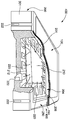
도 1은, 본 발명의 실시예에 따른, 비자성 패키지 몸체에 실링되는 예시적인 비자성 덮개를 포함하는 비자성 패키지의 부분적으로 절개된 투시도(perspective partially sectioned view)이다.
도 2는, 도 1의 비자성 덮개의 부분적으로 절개된 투시도이다.
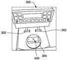
도 3a 내지 도 3c는, 본 발명의 실시예를 제조하기 위해 사용되는 글로브 박스, 타카(tacker), 오븐, 및 심 씰러(seam sealer)의 투시도이다.
도 4는, 도 1의 비자성 덮개와 비자성 패키지 몸체 사이의 심 시일(seam-seal)의 부분적으로 절개된 상세도이다.
Claims (29)
- 비자성 밀봉 패키지(non-magnetic hermetic package)에 있어서,
개방된 캐비티를 둘러싸는 벽 ― 상기 벽의 상부 에지 둘레에, 일반적으로 평면인 비자성의 금속성 시일 링(seal ring)이 연속 루프로 배치됨 ― ;
상기 캐비티 내에 결합되는(bonded) 민감한 컴포넌트(sensitive component); 및
금속성 시일에 의해 상기 캐비티를 폐쇄하기 위해 상기 시일 링에 실링되는(sealed) 비자성 덮개
를 포함하는, 비자성 밀봉 패키지. - 제1항에 있어서,
상기 시일 링은, 패키지 몸체 벽에 결합되는 텅스텐 층, 상기 텅스텐 층 위의 구리 층, 및 상기 구리 층 위의 금 층을 포함하며, 상기 금 층은 상기 금속성 시일에 결합되는 것인, 비자성 밀봉 패키지. - 제1항에 있어서,
상기 시일 링은, 상기 벽에 결합되는 텅스텐 층, 상기 텅스텐 층 위의 구리 층, 상기 구리 층 위의 팔라듐 층, 및 상기 금속성 시일에 결합되는 금 층을 포함하는 것인, 비자성 밀봉 패키지. - 제1항에 있어서,
상기 금속성 시일은 금/주석 솔더에 의해 형성되는 것인, 비자성 밀봉 패키지. - 제1항에 있어서,
상기 민감한 컴포넌트와 전기적으로 연결되는, 상기 캐비티 내부의 전기적 콘택을 더 포함하는, 비자성 밀봉 패키지. - 제5항에 있어서,
상기 패키지 벽 상에 형성되며 상기 캐비티 내부의 상기 전기적 콘택 및 상기 민감한 컴포넌트를 통해 서로 전기적으로 연결되는 외부 핀을 더 포함하고, 상기 민감한 컴포넌트를 통한 상기 외부 핀 사이의 캐패시턴스는 약 2 pF 미만인 것인, 비자성 밀봉 패키지. - 제1항에 있어서,
상기 민감한 컴포넌트는 MEMS 디바이스인 것인, 비자성 밀봉 패키지. - 제7항에 있어서,
상기 MEMS 디바이스는, 번인(burn-in) 이후 1 옴 미만으로 드리프트하는 안정된 온-저항(on-resistance)을 갖는 스위치인 것인, 비자성 밀봉 패키지. - 제7항에 있어서,
상기 MEMS 디바이스는, 적어도 약 250 V의 차단 전압(blocking voltage)을 갖는 스위치인 것인, 비자성 밀봉 패키지. - 제1항에 있어서,
상기 비자성 덮개는, 대략적으로 대기 산소 농도를 갖는 깨끗하고 건조한 공기에서 상기 시일 링에 심 실링되는(seam sealed), 비자성 밀봉 패키지. - 제1항에 있어서,
상기 패키지는 기체 산소를 포함하는, 비자성 밀봉 패키지. - 제11항에 있어서,
상기 패키지는 약 -40℃ 미만의 이슬점을 갖는 깨끗하고 건조한 공기를 포함하는, 비자성 밀봉 패키지. - 제1항에 있어서,
상기 덮개는 비자성인 것인, 비자성 밀봉 패키지. - 제13항에 있어서,
상기 덮개는 금속성인 것인, 비자성 밀봉 패키지. - 제14항에 있어서,
상기 덮개는 몰리브덴을 포함하는 것인, 비자성 밀봉 패키지. - 비자성 패키지에 있어서,
내부 캐비티를 정의하는 벽;
상기 벽의 상부 에지 둘레의 일반적으로 평면인 비자성의 금속성 시일 링; 및
내부로부터 상기 벽을 통해 외부 핀까지 연장하는 상기 내부 캐비티 내의 적어도 하나의 전기적 콘택
을 포함하고,
상기 시일 링은 텅스텐 층, 구리 층, 팔라듐 층, 및 금 층을 포함하는 것인, 비자성 패키지. - 제16항에 있어서,
무플럭스 저온 프로세스(fluxless low temperature process)를 사용하여 상기 캐비티 안으로 결합되는 민감한 컴포넌트를 더 포함하는, 비자성 패키지. - 제17항에 있어서,
상기 결합 프로세스에서 인듐 솔더가 사용되는 것인, 비자성 패키지. - 제18항에 있어서,
상기 결합 프로세스는, 상기 패키지 몸체 내의 상기 민감한 컴포넌트의 스크러빙(scrubbing) 모션을 포함하는 것인, 비자성 패키지. - 제17항에 있어서,
상기 결합 프로세스는 상기 적어도 하나의 전기적 콘택에 대한 상기 민감한 컴포넌트의 초음파 용접을 포함하는 것인, 비자성 패키지. - 비자성 밀봉 패키지를 제조하기 위한 방법에 있어서,
개방된 캐비티를 둘러싸는 벽을 구비하며 상기 벽의 상부 에지 둘레에 비자성이며 일반적으로 평면인 금속성 시일 링을 연속 루프로 구비하는 비자성 세라믹 패키지 몸체를 획득하는 단계;
상기 캐비티 내에서 민감한 컴포넌트를 결합하는 단계; 및
비자성 덮개를 상기 시일 링에 실링하는 단계
를 포함하는, 비자성 밀봉 패키지를 제조하기 위한 방법. - 제21항에 있어서,
상기 민감한 컴포넌트를 결합하는 단계는 무플럭스의 저온 솔더 프로세스를 포함하는 것인, 비자성 밀봉 패키지를 제조하기 위한 방법. - 제22항에 있어서,
상기 저온 솔더로서 인듐이 사용되는 것인, 비자성 밀봉 패키지를 제조하기 위한 방법. - 제21항에 있어서,
상기 결합 프로세스는, 상기 패키지 몸체와 관련한 상기 민감한 컴포넌트의 스크러빙 모션을 포함하는 것인, 비자성 밀봉 패키지를 제조하기 위한 방법. - 제21항에 있어서,
상기 비자성 덮개를 실링하는 단계는 산소 하에서 달성되는 것인, 비자성 밀봉 패키지를 제조하기 위한 방법. - 제21항에 있어서,
상기 비자성 덮개를 실링하는 단계는 심 실링 프로세스인 것인, 비자성 밀봉 패키지를 제조하기 위한 방법. - 제21항에 있어서,
상기 민감한 컴포넌트의 그리고 상기 캐비티의 대향하는 면을, 본질적으로 TiW/Au 또는 W/Cu/Au로 구성되는 비자성의 솔더링 가능한 코팅(non-magnetic solderable coating)으로 미리 코팅하는 단계를 더 포함하는, 비자성 밀봉 패키지를 제조하기 위한 방법. - 제21항에 있어서,
상기 비자성 덮개를 상기 비자성의 금속성 시일 링에 실링하기 이전에 상기 패키지 몸체 및 상기 민감한 컴포넌트를 애싱하고 진공 베이킹하는 단계를 더 포함하는, 비자성 밀봉 패키지를 제조하기 위한 방법. - MEMS 디바이스를 패키지 몸체에 무플럭스 솔더 결합하기 위한 방법에 있어서,
상기 MEMS 디바이스의 그리고 상기 패키지 몸체의 대향하는 면 사이에 인듐 프리폼(preform)을 제공하는 단계;
플럭스 또는 성형 가스(forming gas)를 도입하지 않으면서, 상기 인듐 프리폼을 리플로우 온도 범위 내에서 가열하고 유지하는 단계; 및
상기 인듐 프리폼을 상기 MEMS 디바이스로 그리고 상기 패키지 몸체로 리플로우하여 부착하기 위해 상기 인듐 프리폼에 대해 상기 MEMS 디바이스를 스크러빙하는 단계
를 포함하는, MEMS 디바이스를 패키지 몸체에 무플럭스 솔더 결합하기 위한 방법.
Applications Claiming Priority (3)
| Application Number | Priority Date | Filing Date | Title |
|---|---|---|---|
| US14/529,311 | 2014-10-31 | ||
| US14/529,311 US10431509B2 (en) | 2014-10-31 | 2014-10-31 | Non-magnetic package and method of manufacture |
| PCT/US2015/057517 WO2016069560A1 (en) | 2014-10-31 | 2015-10-27 | Non-magnetic package and method of manufacture |
Publications (2)
| Publication Number | Publication Date |
|---|---|
| KR20170077216A true KR20170077216A (ko) | 2017-07-05 |
| KR102483117B1 KR102483117B1 (ko) | 2022-12-29 |
Family
ID=55853508
Family Applications (1)
| Application Number | Title | Priority Date | Filing Date |
|---|---|---|---|
| KR1020177014781A Active KR102483117B1 (ko) | 2014-10-31 | 2015-10-27 | 비자성 패키지 및 제조 방법 |
Country Status (8)
| Country | Link |
|---|---|
| US (2) | US10431509B2 (ko) |
| EP (1) | EP3213101B1 (ko) |
| JP (1) | JP6629317B2 (ko) |
| KR (1) | KR102483117B1 (ko) |
| CN (1) | CN107004642B (ko) |
| CA (1) | CA2966183C (ko) |
| SG (1) | SG11201703295RA (ko) |
| WO (1) | WO2016069560A1 (ko) |
Families Citing this family (12)
| Publication number | Priority date | Publication date | Assignee | Title |
|---|---|---|---|---|
| US10431509B2 (en) * | 2014-10-31 | 2019-10-01 | General Electric Company | Non-magnetic package and method of manufacture |
| CN106772142A (zh) * | 2016-11-25 | 2017-05-31 | 中国科学院地质与地球物理研究所 | 一种磁通门传感器及其制造方法 |
| US11309251B2 (en) | 2017-07-31 | 2022-04-19 | AdTech Ceramics Company | Selective metallization of integrated circuit packages |
| JP6784317B2 (ja) * | 2018-10-15 | 2020-11-11 | 三菱マテリアル株式会社 | パッケージ用蓋材及びパッケージの製造方法 |
| CN110112039A (zh) * | 2019-05-24 | 2019-08-09 | 中汇瑞德电子(芜湖)有限公司 | 一种密封继电器及其密封方法 |
| US12235144B2 (en) * | 2020-09-17 | 2025-02-25 | Applied Materials, Inc.—Robotics | Micro-electromechanical device for use in a flow control apparatus |
| CN115312549A (zh) * | 2021-05-05 | 2022-11-08 | 胜丽国际股份有限公司 | 传感器封装结构 |
| CN117242567A (zh) * | 2021-05-12 | 2023-12-15 | 三菱电机株式会社 | 气密封装元件以及元件模块 |
| JP7652160B2 (ja) | 2022-09-08 | 2025-03-27 | 株式会社村田製作所 | 電子部品パッケージ及び電子部品パッケージの製造方法 |
| BE1031732B1 (nl) * | 2023-06-22 | 2025-02-03 | C Mac Electromag Bvba | Halfgeleider-afdekking met soldeermateriaalpakking |
| WO2025034788A1 (en) * | 2023-08-10 | 2025-02-13 | Kyocera International, Inc. | Microelectronic package with non-magnetic plating structure |
| JP2025079604A (ja) | 2023-11-10 | 2025-05-22 | 日本特殊陶業株式会社 | 半導体基板 |
Citations (5)
| Publication number | Priority date | Publication date | Assignee | Title |
|---|---|---|---|---|
| KR20020074277A (ko) * | 2001-03-19 | 2002-09-30 | 앰코 테크놀로지 코리아 주식회사 | 반도체 패키지 제조 장치 및 그 방법 |
| US20050012188A1 (en) * | 2001-11-09 | 2005-01-20 | Christian Val | Device for the hermetic encapsulation of a component that must be protected against all stresses |
| KR20070017584A (ko) * | 2002-06-21 | 2007-02-12 | 동경 엘렉트론 주식회사 | Mems 어레이 및 그 제조 방법과, 그것에 기초한mems 디바이스의 제조 방법 |
| US20120177853A1 (en) * | 2010-06-30 | 2012-07-12 | Vectron International Gmbh & Co. Kg | Metallization for a cavity housing and a nonmagnetic sealed cavity housing |
| KR20130100441A (ko) * | 2012-03-02 | 2013-09-11 | 홍익대학교 산학협력단 | 복합구조의 범프를 사용하여 이루어지는 플립칩 패키지의 제조방법 및 이에 의해 제조된 플립칩 패키지 |
Family Cites Families (40)
| Publication number | Priority date | Publication date | Assignee | Title |
|---|---|---|---|---|
| GB1431919A (en) | 1973-08-15 | 1976-04-14 | Atomic Energy Authority Uk | Microcircuit packages |
| US4506108A (en) | 1983-04-01 | 1985-03-19 | Sperry Corporation | Copper body power hybrid package and method of manufacture |
| US4582240A (en) | 1984-02-08 | 1986-04-15 | Gould Inc. | Method for low temperature, low pressure metallic diffusion bonding of piezoelectric components |
| US4659006A (en) * | 1985-09-26 | 1987-04-21 | Rca Corporation | Method of bonding a die to a substrate |
| US4866505A (en) | 1986-03-19 | 1989-09-12 | Analog Devices, Inc. | Aluminum-backed wafer and chip |
| US5178745A (en) | 1991-05-03 | 1993-01-12 | At&T Bell Laboratories | Acidic palladium strike bath |
| US5200640A (en) | 1991-08-12 | 1993-04-06 | Electron Power Inc. | Hermetic package having covers and a base providing for direct electrical connection |
| JPH06125018A (ja) * | 1992-10-14 | 1994-05-06 | Sumitomo Electric Ind Ltd | 半導体素子用キャップ |
| JP3417608B2 (ja) | 1993-08-03 | 2003-06-16 | 日本特殊陶業株式会社 | 半導体パッケージ用のセラミック製リッド基板 |
| US5446316A (en) * | 1994-01-06 | 1995-08-29 | Harris Corporation | Hermetic package for a high power semiconductor device |
| US6390353B1 (en) | 1998-01-06 | 2002-05-21 | Williams Advanced Materials, Inc. | Integral solder and plated sealing cover and method of making the same |
| JP2002353251A (ja) * | 2001-05-22 | 2002-12-06 | Rohm Co Ltd | 半導体素子の実装構造 |
| EP1415328A2 (en) * | 2001-08-01 | 2004-05-06 | Lilogix, Inc. doing business as RD Automation | Process and apparatus for mounting semiconductor components to substrates and parts therefor |
| KR100442830B1 (ko) * | 2001-12-04 | 2004-08-02 | 삼성전자주식회사 | 저온의 산화방지 허메틱 실링 방법 |
| US6962338B2 (en) | 2002-02-22 | 2005-11-08 | Jds Uniphase Inc. | Hermetic seal and a method of making such a hermetic seal |
| JP4088867B2 (ja) | 2002-05-01 | 2008-05-21 | 株式会社リコー | 半導体発光素子の固着方法 |
| US6953985B2 (en) * | 2002-06-12 | 2005-10-11 | Freescale Semiconductor, Inc. | Wafer level MEMS packaging |
| WO2004068189A2 (en) * | 2003-01-27 | 2004-08-12 | David Stark | Hermetic window assemblies and frames |
| US6848610B2 (en) | 2003-03-25 | 2005-02-01 | Intel Corporation | Approaches for fluxless soldering |
| US20040232535A1 (en) * | 2003-05-22 | 2004-11-25 | Terry Tarn | Microelectromechanical device packages with integral heaters |
| US7253029B2 (en) | 2004-03-10 | 2007-08-07 | M/A-Com, Inc. | Non-magnetic, hermetically-sealed micro device package |
| DE112005000051T5 (de) | 2004-11-05 | 2006-08-31 | Neomax Materials Co., Ltd., Suita | Hermetische Abdichtkappe, Verfahren zur Herstellung einer hermetischen Abdichtkappe sowie Aufbewahrungsverpackung für eine elektronische Komponente |
| US7743963B1 (en) | 2005-03-01 | 2010-06-29 | Amerasia International Technology, Inc. | Solderable lid or cover for an electronic circuit |
| US7495462B2 (en) * | 2005-03-24 | 2009-02-24 | Memsic, Inc. | Method of wafer-level packaging using low-aspect ratio through-wafer holes |
| US8786165B2 (en) * | 2005-09-16 | 2014-07-22 | Tsmc Solid State Lighting Ltd. | QFN/SON compatible package with SMT land pads |
| TWI313501B (en) * | 2006-03-22 | 2009-08-11 | Ind Tech Res Inst | A process for manufacture plastic package of mems devices and the structure for the same |
| US7755292B1 (en) | 2007-01-22 | 2010-07-13 | The United States Of America As Represented By The Administrator Of The National Aeronautics And Space Administration | Ultraminiature broadband light source and method of manufacturing same |
| DE112009001079B4 (de) * | 2008-05-02 | 2020-02-06 | Hitachi Metals, Ltd. | Hermetisch abdichtende Kappe |
| JP2009285810A (ja) * | 2008-05-30 | 2009-12-10 | Toshiba Corp | 半導体装置およびその製造方法 |
| US7800190B2 (en) | 2008-06-16 | 2010-09-21 | Honeywell International Inc. | Getter on die in an upper sense plate designed system |
| JP5624058B2 (ja) | 2009-01-30 | 2014-11-12 | ケイアム・コーポレーションKaiam Corp. | マイクロ機構により整列された光学アセンブリ |
| CN201450001U (zh) * | 2009-06-25 | 2010-05-05 | 南京中旭电子科技有限公司 | 高可靠霍尔集成电路无磁性陶瓷气密封装外売结构 |
| US9137903B2 (en) * | 2010-12-21 | 2015-09-15 | Tessera, Inc. | Semiconductor chip assembly and method for making same |
| US8749237B2 (en) * | 2011-01-11 | 2014-06-10 | General Electric Company | Optically controlled MEMS switch and method of using the same |
| WO2012106326A1 (en) | 2011-01-31 | 2012-08-09 | The Regents Of The University Of California | Using millisecond pulsed laser welding in mems packaging |
| US8536663B1 (en) | 2011-04-28 | 2013-09-17 | Amkor Technology, Inc. | Metal mesh lid MEMS package and method |
| JP2013206949A (ja) * | 2012-03-27 | 2013-10-07 | Kyocera Corp | 蓋体およびこれを用いた光半導体素子収納用パッケージ |
| US10211115B2 (en) * | 2014-05-21 | 2019-02-19 | Materion Corporation | Method of making a ceramic combo lid with selective and edge metallizations |
| US10431509B2 (en) * | 2014-10-31 | 2019-10-01 | General Electric Company | Non-magnetic package and method of manufacture |
| US10196745B2 (en) * | 2014-10-31 | 2019-02-05 | General Electric Company | Lid and method for sealing a non-magnetic package |
-
2014
- 2014-10-31 US US14/529,311 patent/US10431509B2/en active Active
-
2015
- 2015-10-27 CN CN201580059055.2A patent/CN107004642B/zh active Active
- 2015-10-27 EP EP15854828.9A patent/EP3213101B1/en active Active
- 2015-10-27 WO PCT/US2015/057517 patent/WO2016069560A1/en not_active Ceased
- 2015-10-27 CA CA2966183A patent/CA2966183C/en active Active
- 2015-10-27 JP JP2017522479A patent/JP6629317B2/ja active Active
- 2015-10-27 KR KR1020177014781A patent/KR102483117B1/ko active Active
- 2015-10-27 SG SG11201703295RA patent/SG11201703295RA/en unknown
-
2018
- 2018-11-30 US US16/205,451 patent/US10804174B2/en active Active
Patent Citations (5)
| Publication number | Priority date | Publication date | Assignee | Title |
|---|---|---|---|---|
| KR20020074277A (ko) * | 2001-03-19 | 2002-09-30 | 앰코 테크놀로지 코리아 주식회사 | 반도체 패키지 제조 장치 및 그 방법 |
| US20050012188A1 (en) * | 2001-11-09 | 2005-01-20 | Christian Val | Device for the hermetic encapsulation of a component that must be protected against all stresses |
| KR20070017584A (ko) * | 2002-06-21 | 2007-02-12 | 동경 엘렉트론 주식회사 | Mems 어레이 및 그 제조 방법과, 그것에 기초한mems 디바이스의 제조 방법 |
| US20120177853A1 (en) * | 2010-06-30 | 2012-07-12 | Vectron International Gmbh & Co. Kg | Metallization for a cavity housing and a nonmagnetic sealed cavity housing |
| KR20130100441A (ko) * | 2012-03-02 | 2013-09-11 | 홍익대학교 산학협력단 | 복합구조의 범프를 사용하여 이루어지는 플립칩 패키지의 제조방법 및 이에 의해 제조된 플립칩 패키지 |
Also Published As
| Publication number | Publication date |
|---|---|
| JP6629317B2 (ja) | 2020-01-15 |
| CN107004642B (zh) | 2020-09-04 |
| JP2017534178A (ja) | 2017-11-16 |
| EP3213101B1 (en) | 2022-05-18 |
| KR102483117B1 (ko) | 2022-12-29 |
| CA2966183C (en) | 2023-03-28 |
| US20190103331A1 (en) | 2019-04-04 |
| EP3213101A1 (en) | 2017-09-06 |
| CN107004642A (zh) | 2017-08-01 |
| EP3213101A4 (en) | 2018-07-04 |
| WO2016069560A1 (en) | 2016-05-06 |
| US10431509B2 (en) | 2019-10-01 |
| CA2966183A1 (en) | 2016-05-06 |
| US10804174B2 (en) | 2020-10-13 |
| US20160126195A1 (en) | 2016-05-05 |
| SG11201703295RA (en) | 2017-05-30 |
Similar Documents
| Publication | Publication Date | Title |
|---|---|---|
| US10804174B2 (en) | Non-magnetic package and method of manufacture | |
| US10208382B2 (en) | Method for making a seam-sealable non-magnetic lid and package | |
| KR20160065864A (ko) | 금속-세라믹 땜납 연결을 생성하는 방법 | |
| CN102017132A (zh) | 气密密封用盖 | |
| JPWO2018066473A1 (ja) | 溶接用電子部品、実装基板及び温度センサ | |
| JP6429266B2 (ja) | 電子部品装置 | |
| JP2000236035A (ja) | 電子部品用パッケージおよび圧電振動デバイス | |
| KR102117466B1 (ko) | 전자부품 패키지 | |
| US6809259B2 (en) | Through terminal and X-ray tube | |
| JP2007012728A (ja) | 圧電振動子パッケージ及びその製造方法ならびに物理量センサー | |
| JP2009117869A (ja) | 機能素子パッケージの製造方法 | |
| JP3401781B2 (ja) | 電子部品用パッケージおよび電子部品用パッケージの製造方法 | |
| US20050121420A1 (en) | Electric welder, electrode and method of use thereof for spot-weld tacking eutectic solder to thin film depositions on non-conductive substrates | |
| JP4799211B2 (ja) | 蓋体およびそれを用いた電子装置 | |
| JP2007043106A (ja) | 気密封止用リッド材およびその製造方法ならびに電子部品用パッケージ | |
| JP2003197797A (ja) | 圧電素子の気密封止方法 |
Legal Events
| Date | Code | Title | Description |
|---|---|---|---|
| PA0105 | International application |
St.27 status event code: A-0-1-A10-A15-nap-PA0105 |
|
| PG1501 | Laying open of application |
St.27 status event code: A-1-1-Q10-Q12-nap-PG1501 |
|
| PA0201 | Request for examination |
St.27 status event code: A-1-2-D10-D11-exm-PA0201 |
|
| E902 | Notification of reason for refusal | ||
| PE0902 | Notice of grounds for rejection |
St.27 status event code: A-1-2-D10-D21-exm-PE0902 |
|
| E13-X000 | Pre-grant limitation requested |
St.27 status event code: A-2-3-E10-E13-lim-X000 |
|
| P11-X000 | Amendment of application requested |
St.27 status event code: A-2-2-P10-P11-nap-X000 |
|
| P13-X000 | Application amended |
St.27 status event code: A-2-2-P10-P13-nap-X000 |
|
| E902 | Notification of reason for refusal | ||
| PE0902 | Notice of grounds for rejection |
St.27 status event code: A-1-2-D10-D21-exm-PE0902 |
|
| P11-X000 | Amendment of application requested |
St.27 status event code: A-2-2-P10-P11-nap-X000 |
|
| P13-X000 | Application amended |
St.27 status event code: A-2-2-P10-P13-nap-X000 |
|
| E701 | Decision to grant or registration of patent right | ||
| PE0701 | Decision of registration |
St.27 status event code: A-1-2-D10-D22-exm-PE0701 |
|
| GRNT | Written decision to grant | ||
| PR0701 | Registration of establishment |
St.27 status event code: A-2-4-F10-F11-exm-PR0701 |
|
| PR1002 | Payment of registration fee |
St.27 status event code: A-2-2-U10-U12-oth-PR1002 Fee payment year number: 1 |
|
| PG1601 | Publication of registration |
St.27 status event code: A-4-4-Q10-Q13-nap-PG1601 |
|
| R18 | Changes to party contact information recorded |
Free format text: ST27 STATUS EVENT CODE: A-5-5-R10-R18-OTH-X000 (AS PROVIDED BY THE NATIONAL OFFICE) |
|
| R18-X000 | Changes to party contact information recorded |
St.27 status event code: A-5-5-R10-R18-oth-X000 |
|
| PR1001 | Payment of annual fee |
St.27 status event code: A-4-4-U10-U11-oth-PR1001 Fee payment year number: 4 |
|
| U11 | Full renewal or maintenance fee paid |
Free format text: ST27 STATUS EVENT CODE: A-4-4-U10-U11-OTH-PR1001 (AS PROVIDED BY THE NATIONAL OFFICE) Year of fee payment: 4 |
|
| P22-X000 | Classification modified |
St.27 status event code: A-4-4-P10-P22-nap-X000 |
|
| P22-X000 | Classification modified |
St.27 status event code: A-4-4-P10-P22-nap-X000 |