KR20170077280A - Copper foil provided with carrier, and copper-clad laminate using said copper foil provided with carrier - Google Patents
Copper foil provided with carrier, and copper-clad laminate using said copper foil provided with carrier Download PDFInfo
- Publication number
- KR20170077280A KR20170077280A KR1020177017436A KR20177017436A KR20170077280A KR 20170077280 A KR20170077280 A KR 20170077280A KR 1020177017436 A KR1020177017436 A KR 1020177017436A KR 20177017436 A KR20177017436 A KR 20177017436A KR 20170077280 A KR20170077280 A KR 20170077280A
- Authority
- KR
- South Korea
- Prior art keywords
- layer
- total amount
- carrier
- copper foil
- resin
- Prior art date
- Legal status (The legal status is an assumption and is not a legal conclusion. Google has not performed a legal analysis and makes no representation as to the accuracy of the status listed.)
- Granted
Links
- 0 C*(OC)SOc1ccc(C)cc1 Chemical compound C*(OC)SOc1ccc(C)cc1 0.000 description 2
Images



Classifications
-
- C—CHEMISTRY; METALLURGY
- C25—ELECTROLYTIC OR ELECTROPHORETIC PROCESSES; APPARATUS THEREFOR
- C25D—PROCESSES FOR THE ELECTROLYTIC OR ELECTROPHORETIC PRODUCTION OF COATINGS; ELECTROFORMING; APPARATUS THEREFOR
- C25D7/00—Electroplating characterised by the article coated
- C25D7/06—Wires; Strips; Foils
- C25D7/0614—Strips or foils
-
- C—CHEMISTRY; METALLURGY
- C25—ELECTROLYTIC OR ELECTROPHORETIC PROCESSES; APPARATUS THEREFOR
- C25D—PROCESSES FOR THE ELECTROLYTIC OR ELECTROPHORETIC PRODUCTION OF COATINGS; ELECTROFORMING; APPARATUS THEREFOR
- C25D5/00—Electroplating characterised by the process; Pretreatment or after-treatment of workpieces
- C25D5/10—Electroplating with more than one layer of the same or of different metals
- C25D5/12—Electroplating with more than one layer of the same or of different metals at least one layer being of nickel or chromium
- C25D5/14—Electroplating with more than one layer of the same or of different metals at least one layer being of nickel or chromium two or more layers being of nickel or chromium, e.g. duplex or triplex layers
-
- C—CHEMISTRY; METALLURGY
- C25—ELECTROLYTIC OR ELECTROPHORETIC PROCESSES; APPARATUS THEREFOR
- C25D—PROCESSES FOR THE ELECTROLYTIC OR ELECTROPHORETIC PRODUCTION OF COATINGS; ELECTROFORMING; APPARATUS THEREFOR
- C25D5/00—Electroplating characterised by the process; Pretreatment or after-treatment of workpieces
- C25D5/60—Electroplating characterised by the structure or texture of the layers
- C25D5/605—Surface topography of the layers, e.g. rough, dendritic or nodular layers
-
- H—ELECTRICITY
- H05—ELECTRIC TECHNIQUES NOT OTHERWISE PROVIDED FOR
- H05K—PRINTED CIRCUITS; CASINGS OR CONSTRUCTIONAL DETAILS OF ELECTRIC APPARATUS; MANUFACTURE OF ASSEMBLAGES OF ELECTRICAL COMPONENTS
- H05K3/00—Apparatus or processes for manufacturing printed circuits
- H05K3/38—Improvement of the adhesion between the insulating substrate and the metal
- H05K3/382—Improvement of the adhesion between the insulating substrate and the metal by special treatment of the metal
-
- H—ELECTRICITY
- H05—ELECTRIC TECHNIQUES NOT OTHERWISE PROVIDED FOR
- H05K—PRINTED CIRCUITS; CASINGS OR CONSTRUCTIONAL DETAILS OF ELECTRIC APPARATUS; MANUFACTURE OF ASSEMBLAGES OF ELECTRICAL COMPONENTS
- H05K3/00—Apparatus or processes for manufacturing printed circuits
- H05K3/38—Improvement of the adhesion between the insulating substrate and the metal
- H05K3/389—Improvement of the adhesion between the insulating substrate and the metal by the use of a coupling agent, e.g. silane
-
- H—ELECTRICITY
- H05—ELECTRIC TECHNIQUES NOT OTHERWISE PROVIDED FOR
- H05K—PRINTED CIRCUITS; CASINGS OR CONSTRUCTIONAL DETAILS OF ELECTRIC APPARATUS; MANUFACTURE OF ASSEMBLAGES OF ELECTRICAL COMPONENTS
- H05K3/00—Apparatus or processes for manufacturing printed circuits
- H05K3/46—Manufacturing multilayer circuits
- H05K3/4644—Manufacturing multilayer circuits by building the multilayer layer by layer, i.e. build-up multilayer circuits
- H05K3/4652—Adding a circuit layer by laminating a metal foil or a preformed metal foil pattern
Landscapes
- Chemical & Material Sciences (AREA)
- Engineering & Computer Science (AREA)
- Chemical Kinetics & Catalysis (AREA)
- Electrochemistry (AREA)
- Materials Engineering (AREA)
- Metallurgy (AREA)
- Organic Chemistry (AREA)
- Manufacturing & Machinery (AREA)
- Microelectronics & Electronic Packaging (AREA)
- Electroplating Methods And Accessories (AREA)
- Parts Printed On Printed Circuit Boards (AREA)
- Laminated Bodies (AREA)
Abstract
동박 또는 구리 합금박 상에, 조화 (트리트) 처리를 실시함으로써 형성된 조화 처리층, 이 조화 처리층 상에 형성된 Ni-Co 층으로 이루어지는 내열층, 및 이 내열층 상에 형성된 Zn, Ni, Cr 을 함유하는 내후층 및 방청층으로 이루어지는 복수의 표면 처리층을 갖고, 상기 표면 처리층 중의 전체 Zn 량/(전체 Zn 량 + 전체 Ni 량) 이 0.02 이상 0.35 이하이고, 상기 표면 처리층 중의 전체 Ni 량이 1600 ㎍/d㎡ 이하인 것을 특징으로 하는 표면 처리층이 부착된 동박. 동박의 표면에 조화 처리를 형성한 후, 그 위에 내열층·방청층을 형성 후, 실란 커플링 처리가 실시된 인쇄 회로용 동박을 사용한 구리 피복 적층판에 있어서, 파인 패턴 인쇄 회로 형성 후에, 기판을 산 처리나 화학 에칭을 실시하였을 때에, 동박 회로와 기판 수지의 계면으로의 산의 스며듦에 의한 밀착성 저하의 억제를 향상시킬 수 있고, 내산성 밀착 강도 우수하고, 또한 알칼리 에칭성이 우수한 캐리어 부착 동박을 제공한다.A harmful treatment layer formed by subjecting a copper foil or a copper alloy foil to a harm treatment (try treatment), a heat-resistant layer comprising a Ni-Co layer formed on the roughened treatment layer, and Zn, Ni and Cr formed on the heat- (Total Zn amount + total Ni amount) in the surface treatment layer is 0.02 or more and 0.35 or less, and the total amount of Ni in the surface treatment layer is 1600 占 퐂 / dm2 or less. A copper clad laminate using a copper foil for a printed circuit which has been subjected to a silane coupling treatment after a roughening treatment is formed on the surface of the copper foil and a heat resistant layer and a rust preventive layer are formed thereon, It is possible to improve the suppression of decrease in adhesion due to permeation of acid to the interface between the copper foil circuit and the substrate resin when the acid treatment or the chemical etching is carried out and to provide a copper foil with a carrier excellent in acid- to provide.
Description
본 발명은 캐리어 부착 동박에 관한 것이다. 보다 상세하게는, 본 발명은 프린트 배선판이나 실드재의 재료로서 사용되는 캐리어 부착 동박에 관한 것이다.The present invention relates to a copper foil with a carrier. More particularly, the present invention relates to a copper foil with a carrier used as a material for a printed wiring board or a shield member.
구리 및 구리 합금박 (이하, 동박이라 칭한다) 은, 전기·전자 관련 산업의 발전에 크게 기여하고 있고, 특히 인쇄 회로재로서 불가결한 존재가 되어 있다. 인쇄 회로용 동박은 일반적으로, 합성 수지 보드, 폴리이미드 필름 등의 기재에 접착제를 개재하여, 또는 접착제를 사용하지 않고 고온 고압하에서 적층 접착하여, 또는, 폴리이미드 전구체를 도포·건조·경화하거나 하여 구리 피복 적층판을 제조하고, 그 후 목적으로 하는 회로를 형성하기 위해서, 레지스트 도포 및 노광 공정을 거쳐 필요한 회로를 인쇄한 후, 불필요부를 제거하는 에칭 처리가 실시된다. Copper and a copper alloy foil (hereinafter referred to as a copper foil) have contributed greatly to the development of the electric and electronic industry, and are indispensable as a printed circuit board. The copper foil for a printed circuit is generally produced by laminating and bonding a substrate such as a synthetic resin board or a polyimide film with an adhesive or without using an adhesive under high temperature and high pressure or by applying a polyimide precursor, A copper clad laminate is manufactured, and then a necessary circuit is printed through a resist coating and an exposing process in order to form a desired circuit, and then an etching process for removing unnecessary portions is performed.
최종적으로, 필요한 소자가 납땜되어, 일렉트로닉스 디바이스용의 여러 가지 인쇄 회로판을 형성한다. 인쇄 회로판용 동박은, 수지 기재와 접착되는 면 (조화면 (粗化面)) 과 비접착면 (광택면) 으로 상이한데, 각각 많은 방법이 제창되어 있다.Finally, the necessary elements are soldered to form various printed circuit boards for electronics devices. The copper foil for a printed circuit board differs in the surface (roughened surface) to be adhered to the resin base material and the non-adhered surface (glossy surface), and many methods are proposed respectively.
예를 들어, 동박에 형성되는 조화면에 대한 요구로는, 주로, 1) 보존시에 있어서의 산화 변색이 없을 것, 2) 기재와의 박리 강도가 고온 가열, 습식 처리, 납땜, 약품 처리 등의 후에도 충분할 것, 3) 기재와의 적층, 에칭 후에 생기는, 이른바 적층 오점이 없을 것 등을 들 수 있다.For example, the demand for roughened surfaces formed on the copper foil is mainly caused by: 1) there is no oxidation discoloration during storage; 2) the peeling strength with the substrate is high temperature heating, wet processing, brazing, (3) lamination with the substrate, and no so-called stacking fault after etching.
동박의 조화 처리는, 동박과 기재의 접착성을 결정하는 것으로서 큰 역할을 담당하고 있다. 이 조화 처리로는, 당초 구리를 전착하는 구리 조화 처리가 채용되어 있었지만, 그 후 다양한 기술이 제창되어, 내열 박리 강도, 내염산성 및 내산화성의 개선을 목적으로 하여 구리-니켈 조화 처리가 하나의 대표적 처리 방법으로서 정착하게 되었다.The roughening treatment of the copper foil plays a large role in determining the adhesion between the copper foil and the substrate. In this roughening treatment, copper roughening treatment for electrodepositing copper at first is adopted, but various techniques have been developed thereafter. For the purpose of improving heat-resisting peel strength, hydrochloric acid resistance and oxidation resistance, copper- And became a representative processing method.
본건 출원인은, 구리-니켈 조화 처리를 제창하고 (특허문헌 1 참조), 성과를 내어 왔다. 구리-니켈 처리 표면은 흑색을 나타내고, 특히 플렉시블 기판용 압연 처리박에서는, 이 구리-니켈 처리의 흑색이 상품으로서의 심볼로서 인정되기에 이르렀다.The applicant of the present application proposed a copper-nickel coarsening treatment (see Patent Document 1), and has achieved results. The copper-nickel-treated surface exhibited black color, and in the case of the rolled treated foil for a flexible substrate in particular, the copper-nickel-treated black color was recognized as a commodity as a commodity.
그러나, 구리-니켈 조화 처리는, 내열 박리 강도 및 내산화성 그리고 내염산성이 우수한 반면, 최근 파인 패턴용 처리로서 중요해져 온 알칼리 에칭액에 의한 에칭이 곤란하여, 150 ㎛ 피치 회로폭 이하의 파인 패턴 형성시에 처리층이 에칭 나머지가 되어 버린다. However, copper-nickel plating treatment is excellent in heat peel strength, oxidation resistance and hydrochloric acid resistance, while etching with an alkaline etching solution, which has recently become important as a treatment for fine patterning, is difficult and fine pattern formation The treatment layer becomes the etch residue.
그래서, 파인 패턴용 처리로서, 본건 출원인은, 먼저 Cu-Co 처리 (특허문헌 2 및 특허문헌 3 참조) 및 Cu-Co-Ni 처리 (특허문헌 4 참조) 를 개발하였다.Thus, as the treatment for the fine pattern, the Applicant has developed Cu-Co treatment (see Patent Document 2 and Patent Document 3) and Cu-Co-Ni treatment (see Patent Document 4).
이들 조화 처리는, 에칭성, 알칼리 에칭성 및 내염산성에 대해서는 양호하였지만, 아크릴계 접착제를 사용했을 때의 내열 박리 강도가 저하되는 것이 다시 판명되었고, 또 내산화성도 소기 (所期) 만큼 충분하지 않고 그리고 색조도 흑색까지는 도달하지 않아, 갈색 내지 짙은 갈색이었다.These coarsening treatments were good in terms of the etching property, the alkali etching property and the hydrochloric acid resistance, but it was again proved that the heat peeling strength was lowered when the acrylic adhesive was used, and the oxidation resistance was not sufficient in the expected period And color tone did not reach to black, and it was brown to dark brown.
이러한 요망에 따라, 본 출원인은, 동박의 표면에 구리-코발트-니켈 합금 도금에 의한 조화 처리 후, 코발트 도금층 혹은 코발트-니켈 합금 도금층을 형성함으로써, 인쇄 회로용 동박으로서 상기 서술한 많은 일반적 특성을 구비하는 것은 물론, 특히 Cu-Ni 처리와 필적하는 상기 서술한 제특성을 구비하고, 게다가 아크릴계 접착제를 사용했을 때의 내열 박리 강도를 저하시키지 않고, 내산화성이 우수하고 그리고 표면 색조도 흑색인 동박 처리 방법을 개발하는 것에 성공하였다 (특허문헌 5 참조).According to this demand, the present applicant has found that by forming a cobalt plated layer or a cobalt-nickel alloy plated layer on the surface of a copper foil after roughening treatment by copper-cobalt-nickel alloy plating, A copper foil having an excellent oxidation resistance and a black color on the surface of the copper foil, which does not deteriorate the heat peel strength when the acrylic adhesive is used, and which has the above- (See Patent Document 5).
또한, 전자 기기의 발전이 진행되는 가운데 동박 회로 기판의 내열 박리성 향상의 요구가 엄격해졌기 때문에, 본 출원인은, 동박의 표면에 구리-코발트-니켈 합금 도금에 의한 조화 처리 후, 코발트-니켈 합금 도금층을 형성하고, 추가로 아연-니켈 합금 도금층을 형성하는, 내열성이 우수한 인쇄용 동박 처리 방법을 개발하는 것에 성공하였다 (특허문헌 6 참조). 이것은 매우 유효한 발명이며, 오늘날 동박 회로 재료의 주요 제품의 하나로 되어 있다.In addition, since the demand for improvement of the heat peelability of the copper foil circuit board has become stricter in the progress of the development of electronic devices, the present applicant has found that after the copper foil surface is roughened by copper-cobalt-nickel alloy plating, (Refer to Patent Document 6), which is excellent in heat resistance, in which a zinc-nickel alloy plating layer is formed, and further a zinc-nickel alloy plating layer is formed. This is a very effective invention and today it is one of the main products of copper foil circuit material.
그 후, 전자 기기의 발전에 의해 반도체 디바이스의 소형화, 고집적화가 더욱 진행되어, FPC 의 다층 기판 기술이 급속히 진전되었다. 이 FPC 다층 기판의 제조 공정에 있어서는, 구리 피복 적층판으로 파인 패턴 회로 형성 후에, 레지스트 필름 압착 공정이나 금속 도금 공정에 있어서의 동박 회로 기판을 청정화하기 위한 전처리로서, 황산과 과산화수소를 함유하는 에칭액이나, 황산 수용액을 사용한 용액 등에 의한 복수 회의 표면 에칭 처리가 사용되게 되었다.Since then, miniaturization and high integration of semiconductor devices have progressed owing to the development of electronic devices, and the technology of multi-layer substrate of FPC has progressed rapidly. In the manufacturing process of the FPC multi-layer substrate, an etching solution containing sulfuric acid and hydrogen peroxide, or an etching solution containing sulfuric acid and hydrogen peroxide as a pretreatment for cleaning the copper foil circuit board in the resist film pressing step or the metal plating step after formation of a fine pattern circuit with a copper- A plurality of surface etching processes using a solution using an aqueous solution of sulfuric acid or the like have been used.
그런데 상기 FPC 다층판 제조 공정에 있어서의 표면 에칭 처리에 있어서, 특허문헌 6 에 참조되는 동박의 표면에 구리-코발트-니켈 합금 도금에 의한 조화 처리 후, 코발트-니켈 합금 도금층을 형성하고, 추가로 아연-니켈 합금 도금층을 형성하는 인쇄용 동박을 사용한 구리 피복 적층판의 파인 패턴 회로에 있어서, 동박 회로와 기판 수지의 계면을 표면 에칭액이 침식하여, 동박 회로와 기판 수지의 밀착성이 저하되어 버려, FPC 특성으로서 전기 회로 불량을 발생시킨다는 문제가 발생했기 때문에, 이것을 해결하는 것이 요구되고 있다.However, in the surface etching treatment in the FPC multilayered plate manufacturing process, the surface of the copper foil referred to in Patent Document 6 is subjected to a roughening treatment by copper-cobalt-nickel alloy plating, a cobalt-nickel alloy plating layer is formed, In the fine pattern circuit of the copper clad laminate using the printing-use copper foil for forming the zinc-nickel alloy plating layer, the surface etchant is eroded at the interface between the copper foil circuit and the substrate resin and the adhesion between the copper foil circuit and the substrate resin is lowered, It is required to solve this problem.
본 출원인은, 하기 특허문헌 7 에, 동박의 표면에, 구리-코발트-니켈 합금 도금에 의한 조화 처리층, 이 조화 처리층 상에 형성한 코발트-니켈 합금 도금층 및 이 코발트-니켈 합금 도금층 상에, 아연-니켈 합금 도금층을 형성한 인쇄 회로용 동박에 있어서, 아연-니켈 합금 도금층의 총량, 니켈량, 니켈의 비율을 기정 (旣定) 한 기술을 제안하였다.The applicant of the present invention has disclosed in Patent Document 7 the following Patent Document 7 discloses a method for manufacturing a copper-chromium-nickel alloy plating layer, , A zinc-nickel alloy plating layer is formed on a copper foil for a printed circuit, and the total amount of the zinc-nickel alloy plating layer, the amount of nickel, and the ratio of nickel are defined.
이 기술은 유효하지만, Ni 는 아연-니켈 합금층뿐만 아니라, 조화 처리층, 내열층, 내후층 모두에 함유시키는 것이 가능하기 때문에, 표면 에칭에 있어서의 회로 침식 방지, 및 일반적인 FPC 특성에 매우 우수한 효과를 발휘할 수 있는 인쇄 회로용 동박을 얻기 위해서는, 조화 처리층, 내열층, 및 내후층 모두의 전체 Ni 량을 더욱 검토할 필요가 있는 것을 알았다. Although this technique is effective, since Ni can be contained not only in the zinc-nickel alloy layer but also in the roughened layer, the heat resistant layer and the inner layer, it is possible to prevent circuit erosion in surface etching, In order to obtain a copper foil for a printed circuit that can exert its effect, it has been found that it is necessary to further examine the total amount of Ni in both the coarsened layer, the heat resistant layer and the inner layer.
또한 Zn 은 아연-니켈 합금층뿐만 아니라, 내후층, 방청층 모두에 함유시키는 것이 가능하기 때문에, 내후층, 방청층 모두의 전체 Zn 량에 대해, 나아가서는 상기 전체 Ni 량과의 비율에 대해 검토할 필요가 있는 것을 알았다.Since Zn can be contained not only in the zinc-nickel alloy layer but also in both the inner layer and the rust-preventive layer, the ratio of the total amount of Ni to the total amount of Zn in both the inner layer and the rust- I knew I needed to do it.
프린트 배선판은 동박에 절연 기판을 접착시켜 구리 피복 적층판으로 한 후에, 에칭에 의해 동박면에 도체 패턴을 형성한다는 공정을 거쳐 제조되는 것이 일반적이다. 최근 전자 기기의 소형화, 고성능화 요구의 증대에 수반하여 탑재 부품의 고밀도 실장화나 신호의 고주파화가 진전되고, 프린트 배선판에 대해 도체 패턴의 미세화 (파인 피치화) 나 고주파 대응 등이 요구되고 있다.The printed wiring board is generally manufactured through a step of bonding an insulating substrate to a copper foil to form a copper clad laminate, and then forming a conductor pattern on the copper foil surface by etching. In recent years, along with an increase in the demand for miniaturization and high performance of electronic devices, mounting of high-density mounting parts and high frequency signals have progressed, and a printed circuit board has been required to have finer conductor patterns (fine pitch) and high frequency response.
파인 피치화에 대응하여, 최근에는 두께 9 ㎛ 이하, 나아가서는 두께 5 ㎛ 이하의 동박이 요구되고 있지만, 이와 같은 극박의 동박은 기계적 강도가 낮아 프린트 배선판의 제조시에 깨지거나, 주름이 발생하거나 하기 쉽기 때문에, 두께가 있는 금속박을 캐리어로서 이용하고, 이것에 박리층을 개재하여 극박 구리층을 전착시킨 캐리어 부착 동박이 등장하고 있다. 극박 구리층의 표면을 절연 기판에 첩합 (貼合) 하여 열 압착 후에, 캐리어를 박리층을 개재하여 박리한다는 것이 캐리어 부착 동박의 일반적인 사용 방법이다.In response to the fine pitching, a copper foil having a thickness of 9 占 퐉 or less and further having a thickness of 5 占 퐉 or less is required in recent years. However, such a copper foil with a very thin foil has low mechanical strength and is cracked, wrinkled A copper foil with a carrier in which a thin metal foil is used as a carrier and an extremely thin copper layer is electrodeposited with a release layer interposed therebetween has appeared. The surface of the ultra-thin copper layer is bonded to an insulating substrate, and after the thermocompression bonding, the carrier is peeled off through the peeling layer.
여기서, 수지와의 접착면이 되는 캐리어 부착 동박의 극박 구리층의 면에 대해서는, 주로, 극박 구리층과 수지 기재의 박리 강도가 충분한 것, 그리고 그 박리 강도가 고온 가열, 습식 처리, 납땜, 약품 처리 등의 후에도 충분히 유지되고 있는 것이 요구된다.Here, regarding the surface of the ultra-thin copper layer of the copper foil with a carrier to be bonded to the resin, the peeling strength between the ultra-thin copper layer and the resin substrate is sufficient, and the peel strength thereof is high temperature heating, wet processing, It is required to be sufficiently retained even after treatment or the like.
극박 구리층과 수지 기재 사이의 박리 강도를 높이는 방법으로는, 일반적으로, 표면의 프로파일 (요철, 거칠기) 을 크게 한 극박 구리층 상에 다량의 조화 입자를 부착시키는 방법이 대표적이다.As a method of increasing the peeling strength between the ultra-thin copper layer and the resin substrate, a method of attaching a large amount of coarse particles on the ultra-thin copper layer having a generally increased profile (unevenness and roughness) of the surface is typical.
그러나, 프린트 배선판 중에서도 특히 미세한 회로 패턴을 형성할 필요가 있는 반도체 패키지 기판에, 이와 같은 프로파일 (요철, 거칠기) 이 큰 극박 구리층을 사용하면, 회로 에칭시에 불필요한 구리 입자가 남아 버려, 회로 패턴 사이의 절연 불량 등의 문제가 발생한다.However, when a very thin copper layer having such a profile (irregularity and roughness) is used for a semiconductor package substrate which needs to form a particularly fine circuit pattern among printed wiring boards, unnecessary copper particles remain in circuit etching, And the like.
이 때문에, 반도체 패키지 기판을 비롯한 미세 회로 용도의 캐리어 부착 동박으로는, 극박 구리층의 표면에 조화 처리를 실시하지 않은 캐리어 부착 동박을 사용하는 것이 시도되고 있다. 이와 같은 조화 처리를 실시하지 않은 극박 구리층과 수지의 밀착성 (박리 강도) 은, 그 낮은 프로파일 (요철, 조도, 거칠기) 의 영향으로 일반적인 프린트 배선판용 동박과 비교하면 저하되는 경향이 있다. (특허문헌 8) For this reason, it has been attempted to use a copper foil with a carrier not subjected to a roughening treatment on the surface of the ultra-thin copper layer as a copper foil with a carrier for use in a fine circuit including a semiconductor package substrate. The adhesion (peel strength) between the ultra-thin copper layer and the resin not subjected to such roughening treatment tends to be lowered as compared with a general copper foil for a printed wiring board due to its low profile (unevenness, roughness and roughness). (Patent Document 8)
그 때문에, 캐리어 부착 동박에 대해 추가적인 개선이 요구되고 있다.Therefore, further improvement is required for the copper foil with a carrier.
본 발명은 캐리어 부착 동박 및 구리 피복 적층판에 관한 것이며, 특히 동박의 표면에 조화 처리를 형성한 후, 그 위에 내열층·내후층·방청층을 형성 후, 실란 커플링 처리가 실시된 캐리어 부착 동박을 사용한 구리 피복 적층판에 있어서, 파인 패턴 인쇄 회로 형성 후에, 기판을 산 처리나 화학 에칭을 실시하였을 때에, 동박 회로와 기판 수지의 계면으로의 산의 「스며듦」 에 의한 밀착성 저하의 억제를 향상시킬 수 있고, 내산성 밀착 강도 우수하고, 또한 알칼리 에칭성이 우수한 캐리어 부착 동박에 관한 것이다.The present invention relates to a copper foil with a carrier and a copper clad laminate, and more particularly to a copper foil with a carrier and a copper clad laminate having a copper foil coated with a carrier to which a silane coupling treatment has been applied after forming a heat resistant layer, It is possible to improve the suppression of the decrease in adhesion due to " penetration " of the acid at the interface between the copper foil circuit and the substrate resin when the substrate is subjected to the acid treatment or the chemical etching after the formation of the fine pattern printed circuit To a copper foil with a carrier excellent in acid resistance and excellent in alkali etching property.
전자 기기의 발전이 진행되는 가운데, 반도체 디바이스의 소형화, 고집적화가 더욱 진행되어, 이들 인쇄 회로의 제조 공정에서 실시되는 처리가 한층 엄격히 요구되고 있다. 본원 발명은 이들 요구에 부응하는 기술을 제공하는 것을 과제로 한다.As the development of electronic devices progresses, miniaturization and high integration of semiconductor devices are further advanced, and processing performed in the manufacturing process of these printed circuits is more strictly demanded. It is an object of the present invention to provide a technique that meets these needs.
이상으로부터, 본원은 다음의 발명을 제공한다.From the above, the present invention provides the following invention.
1) 동박 또는 구리 합금박 상에, 조화 (트리트) 처리를 실시함으로써 형성된 조화 처리층, 이 조화 처리층 상에 형성된 Ni-Co 층으로 이루어지는 내열층, 및 이 내열층 상에 형성된 Zn, Ni, Cr 을 함유하는 내후층 및 방청층을 갖는 표면 처리층을 갖고, 상기 표면 처리층 중의 전체 Zn 량/(전체 Zn 량 + 전체 Ni 량) 이 0.02 이상 0.35 이하이고, 상기 표면 처리층 중의 전체 Ni 량이 1600 ㎍/d㎡ 이하인 것을 특징으로 하는 캐리어 부착 동박.1) A heat-resistant layer comprising a roughened treatment layer formed by subjecting a copper foil or a copper alloy foil to a treatment (treatment), a Ni-Co layer formed on the roughened treatment layer, Cr and a rust preventive layer, wherein the total amount of Zn / (total amount of Zn + total amount of Ni) in the surface treatment layer is 0.02 or more and 0.35 or less, and the total amount of Ni in the surface- 1600 占 퐂 / dm2 or less.
2) 상기 표면 처리층 중의 전체 Zn 량/(전체 Zn 량 + 전체 Ni 량) 이 0.02 이상 0.23 이하이고, 상기 표면 처리층 중의 전체 Ni 량이 1150 ㎍/d㎡ 이하인 것을 특징으로 하는, 1) 에 기재된 캐리어 부착 동박.2) The method according to 1), wherein the total amount of Zn in the surface-treated layer / total Zn amount + total Ni amount is 0.02 or more and 0.23 or less, and the total amount of Ni in the surface treatment layer is 1150 占 퐂 / Copper with a carrier.
3) 상기 표면 처리층 중의 전체 Ni 량이 350 ∼ 1350 ㎍/d㎡ 인 것을 특징으로 하는 1) 또는 2) 에 기재된 캐리어 부착 동박.3) The copper foil with a carrier according to 1) or 2), wherein the total amount of Ni in the surface treatment layer is 350 to 1350 占 퐂 / dm2.
4) 상기 표면 처리층 중의 전체 Ni 량이 450 ∼ 1100 ㎍/d㎡ 인 것을 특징으로 하는 상기 1) ∼ 3) 중 어느 한 항에 기재된 캐리어 부착 동박.4) The copper foil with a carrier according to any one of 1) to 3) above, wherein the total amount of Ni in the surface treatment layer is 450 to 1100 占 퐂 / dm2.
5) 상기 표면 처리층 중의 전체 Co 량이 770 ∼ 3200 ㎍/d㎡ 이고, 전체 Co 량/(전체 Zn 량 + 전체 Ni 량) 이 3.4 이하인 것을 특징으로 하는 1) ∼ 4) 중 어느 한 항에 기재된 캐리어 부착 동박.(5) The method according to any one of (1) to (4) above, which is characterized in that the total amount of Co in the surface treatment layer is 770 to 3200 쨉 g / dm 2 and the total amount of Co / (total amount of Zn + total amount of Ni) Copper with a carrier.
6) 상기 표면 처리층 중의 전체 Co 량이 770 ∼ 2500 ㎍/d㎡ 이고, 전체 Co 량/(전체 Zn 량 + 전체 Ni 량) 가 3.0 이하인 것을 특징으로 하는 상기 1) ∼ 5) 중 어느 한 항에 기재된 캐리어 부착 동박.6) The method according to any one of 1) to 5) above, wherein the total amount of Co in the surface treatment layer is 770 to 2500 占 퐂 / dm2 and the total amount of Co / (total amount of Zn + total amount of Ni) ≪ / RTI >
7) 상기 표면 처리층 중의 전체 Cr 량이 50 ∼ 120 ㎍/d㎡ 인 것을 특징으로 하는 상기 1) ∼ 6) 중 어느 한 항에 기재된 캐리어 부착 동박.7) The copper foil with a carrier according to any one of 1) to 6) above, wherein the total amount of Cr in the surface treatment layer is 50 to 120 占 퐂 / dm2.
또, 본원은 다음의 발명을 제공한다.The present invention also provides the following invention.
8) 상기 조화 처리층의 Ni 가 50 ∼ 550 ㎍/d㎡ 인 것을 특징으로 하는 상기 1) ∼ 7) 중 어느 한 항에 기재된 캐리어 부착 동박.8) The copper foil with a carrier according to any one of 1) to 7) above, wherein the coarsened layer has Ni of 50 to 550 占 퐂 / dm2.
9) 상기 조화 처리층이 Co, Cu, Ni 의 원소로 이루어지는 조화 처리층인 것을 특징으로 하는 상기 1) ∼ 8) 중 어느 하나에 기재된 캐리어 부착 동박.(9) The copper foil with a carrier according to any one of (1) to (8) above, wherein the roughening treatment layer is a roughened treatment layer made of elements of Co, Cu and Ni.
10) 상기 조화 처리층이 평균 입자경 0.05 ∼ 0.60 ㎛ 의 미세 입자로 이루어지는 것을 특징으로 하는 1) ∼ 9) 중 어느 한 항에 기재된 캐리어 부착 동박.10) The copper foil with a carrier according to any one of 1) to 9), wherein the roughening treatment layer is composed of fine particles having an average particle diameter of 0.05 to 0.60 μm.
11) 상기 조화 처리층이 평균 입자경 0.05 ∼ 0.60 ㎛ 의 Cu, Co, Ni 로 이루어지는 3 원계 합금의 미세 입자로 이루어지는 것을 특징으로 하는 상기 1) ∼ 10) 중 어느 한 항에 기재된 캐리어 부착 동박.(11) The copper foil with a carrier according to any one of (1) to (10) above, wherein the roughening treatment layer is composed of fine particles of a ternary alloy comprising Cu, Co and Ni having an average particle size of 0.05 to 0.60 μm.
12) 상기 조화 처리층이, 평균 입자경 0.25 ∼ 0.45 ㎛ 의 1 차 입자층과, 그 위에 형성된 평균 입자경이 0.05 ∼ 0.25 ㎛ 인 2 차 입자층으로 이루어지는 것을 특징으로 하는 1) ∼ 11) 중 어느 한 항에 기재된 캐리어 부착 동박.(12) The method according to any one of (1) to (11), wherein the harmonizing treatment layer is composed of a primary particle layer having an average particle diameter of 0.25 to 0.45 μm and a secondary particle layer having an average particle diameter of 0.05 to 0.25 μm formed thereon ≪ / RTI >
13) 상기 조화 처리층이, 평균 입자경 0.25 ∼ 0.45 ㎛ 의 Cu 의 1 차 입자층과, 그 위에 형성된 평균 입자경이 0.05 ∼ 0.25 ㎛ 인 Cu, Co, Ni 로 이루어지는 3 원계 합금으로 이루어지는 2 차 입자층으로 이루어지는 것을 특징으로 하는 상기 1) ∼ 12) 중 어느 한 항에 기재된 캐리어 부착 동박.(13) The method according to any one of the above items (1) to (3), wherein the roughening treatment layer comprises a primary particle layer of Cu having an average particle diameter of 0.25 to 0.45 탆 and a secondary particle layer composed of a ternary alloy composed of Cu, Co and Ni having an average particle diameter of 0.05 to 0.25 탆 The copper foil with a carrier according to any one of 1) to 12) above,
14) 상기 1) ∼ 13) 중 어느 한 항에 기재된 캐리어 부착 동박의 상기 극박 구리층으로 이루어지는 인쇄 회로용 동박.14) A copper foil for a printed circuit comprising the ultra-thin copper layer of the copper foil with a carrier according to any one of 1) to 13) above.
15) 상기 표면 처리층 상에 수지층을 구비하는 1) ∼ 13) 중 어느 한 항에 기재된 캐리어 부착 동박.15) The copper foil with a carrier according to any one of 1) to 13), which has a resin layer on the surface treatment layer.
16) 상기 14) 기재의 인쇄 회로용 동박을 수지 기판에 적층 접착한 구리 피복 적층판.16) A copper clad laminate according to item 14), wherein the copper foil for a printed circuit is laminated and bonded to a resin substrate.
17) 상기 1) ∼ 13) 중 어느 한 항에 기재된 캐리어 부착 동박을 사용하여 제조한 프린트 배선판.(17) A printed wiring board produced by using the copper foil with a carrier according to any one of (1) to (13).
18) 상기 1) ∼ 13) 중 어느 한 항에 기재된 캐리어 부착 동박을 사용하여 제조한 프린트 회로판.(18) A printed circuit board manufactured by using the copper foil with a carrier according to any one of (1) to (13).
19) 상기 1) ∼ 13) 중 어느 한 항에 기재된 캐리어 부착 동박을 사용하여 제조한 구리 피복 적층판.(19) A copper clad laminate produced by using the copper foil with a carrier according to any one of (1) to (13).
20) 상기 1) ∼ 13) 중 어느 한 항에 기재된 캐리어 부착 동박과 절연 기판을 준비하는 공정,20) A method for manufacturing a semiconductor device, comprising the steps of: preparing the copper foil with a carrier and the insulating substrate according to any one of 1) to 13)
상기 캐리어 부착 동박과 절연 기판을 적층하는 공정,A step of laminating the copper foil with a carrier and an insulating substrate,
상기 캐리어 부착 동박과 절연 기판을 적층한 후에, 상기 캐리어 부착 동박의 캐리어를 박리하는 공정을 거쳐 구리 피복 적층판을 형성하고, After the step of laminating the carrier-bonded copper foil with the insulating substrate and the step of peeling the carrier of the carrier-coated copper foil, a copper clad laminate is formed,
그 후, 세미 애디티브법, 서브트랙티브법, 파틀리 애디티브법 또는 모디파이드 세미 애디티브법 중 어느 방법에 의해 회로를 형성하는 공정Thereafter, a step of forming a circuit by any one of the semi-additive method, the subtractive method, the protein additive method, and the modified semi-
을 포함하는 프린트 배선판의 제조 방법.Wherein the step of forming the printed wiring board comprises the steps of:
21) 상기 1) ∼ 13) 중 어느 한 항에 기재된 캐리어 부착 동박의 상기 극박 구리층측 표면에 회로를 형성하는 공정,(21) a step of forming a circuit on the surface of the ultra-thin copper layer side of the copper foil with a carrier according to any one of (1) to (13)
상기 회로가 매몰하도록 상기 캐리어 부착 동박의 상기 극박 구리층측 표면에 수지층을 형성하는 공정, A step of forming a resin layer on the surface of the ultra thin copper layer side of the copper foil with a carrier so that the circuit is buried,
상기 수지층 상에 회로를 형성하는 공정,A step of forming a circuit on the resin layer,
상기 수지층 상에 회로를 형성한 후에, 상기 캐리어를 박리시키는 공정, 및, A step of forming a circuit on the resin layer and thereafter peeling the carrier,
상기 캐리어를 박리시킨 후에, 상기 극박 구리층을 제거함으로써, 상기 극박 구리층측 표면에 형성한, 상기 수지층에 매몰되어 있는 회로를 노출시키는 공정을 포함하는 프린트 배선판의 제조 방법.Exposing a circuit buried in the resin layer formed on the extremely thin copper layer side surface by removing the extremely thin copper layer after peeling the carrier.
22) 상기 수지층 상에 회로를 형성하는 공정이,22) A process for forming a circuit on the resin layer,
상기 수지층 상에 다른 캐리어 부착 동박을 극박 구리층측으로부터 첩합하고, 상기 수지층에 첩합한 캐리어 부착 동박을 사용하여 상기 회로를 형성하는 공정인, 21) 에 기재된 프린트 배선판의 제조 방법.And the other copper-coated copper foil on the resin layer is laminated from the ultra-thin copper layer side, and the circuit is formed by using the copper foil with a carrier bonded to the resin layer.
23) 상기 수지층 상에 첩합하는 캐리어 부착 동박이 1) ∼ 13) 중 어느 한 항에 기재된 캐리어 부착 동박인, 22) 에 기재된 프린트 배선판의 제조 방법.(23) A copper foil with a carrier to be bonded onto the resin layer, wherein the copper foil is a copper foil with a carrier according to any one of (1) to (13).
24) 상기 수지층 상에 회로를 형성하는 공정이 세미 애디티브법, 서브트랙티브법, 파틀리 애디티브법 또는 모디파이드 세미 애디티브법 중 어느 방법에 의해 실시되는, 21) ∼ 23) 중 어느 한 항에 기재된 프린트 배선판의 제조 방법.(24) The process for producing a circuit according to any one of (21) to (23), wherein the step of forming a circuit on the resin layer is carried out by any one of a semiadditive method, a subtractive method, a patelly additive method and a modified semi- A method for producing a printed wiring board according to any one of claims 1 to 5.
25) 캐리어를 박리하기 전에, 캐리어 부착 동박의 캐리어측 표면에 기판을 형성하는 공정을 추가로 포함하는 21) ∼ 24) 중 어느 한 항에 기재된 프린트 배선판의 제조 방법.(25) The method for producing a printed wiring board according to any one of (21) to (24), further comprising a step of forming a substrate on the carrier-side surface of the copper foil with a carrier before peeling off the carrier.
본 발명은 인쇄 회로용 동박 및 구리 피복 적층판용의 캐리어 부착 동박에 관한 것이며, 특히 캐리어, 중간층, 극박 구리층이 이 순서로 적층되어 있는 캐리어 부착 동박의 상기 극박 구리층의 표면에 조화 처리를 형성한 후, 그 위에 내열층·내후층·방청층을 형성 후, 실란 커플링 처리가 실시된 캐리어 부착 동박의 극박 구리층을 사용한 구리 피복 적층판에 있어서, 파인 패턴 인쇄 회로 형성 후에, 기판을 산 처리나 화학 에칭을 실시하였을 때에, 동박 회로와 기판 수지의 계면으로의 산의 「스며듦」 에 의한 밀착성 저하의 억제를 향상시킬 수 있고, 내산성 밀착 강도 우수하고, 또한 알칼리 에칭성이 우수한 캐리어 부착 동박에 관한 것이다.The present invention relates to a copper foil for a printed circuit and a copper foil with a carrier for a copper clad laminate, and more particularly to a copper foil with a carrier, an intermediate layer and an ultra-thin copper layer laminated in this order, In which a heat resistant layer, an inner layer and an anticorrosion layer are formed thereon, and then a silane coupling treatment is applied to the copper clad laminate, It is possible to improve the suppression of the adhesion deterioration due to " permeation " of the acid to the interface between the copper foil circuit and the substrate resin, and to provide a copper foil with a carrier excellent in acid- .
전자 기기의 발전이 진행되는 가운데, 반도체 디바이스의 소형화, 고집적화가 더욱 진행되어, 이들 인쇄 회로의 제조 공정에서 실시되는 처리가 한층 엄격히 요구되고 있다. 본원 발명은 이들 요구에 부응하는 우수한 기술이다.As the development of electronic devices progresses, miniaturization and high integration of semiconductor devices are further advanced, and processing performed in the manufacturing process of these printed circuits is more strictly demanded. The present invention is an excellent technique to meet these demands.
도 1 은, 과산화수소와 황산 용액을 사용하여 표면 에칭했을 경우의, 동박 회로 주변으로부터, 에칭액이 침식했을 경우의 모습 나타내는 설명도이다.
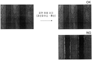
도 2 는, 파인 패턴 인쇄 회로 형성 후에, 기판을 표면 에칭 (과산화수소와 황산의 용액에 의한) 했을 경우의, 동박 회로와 기판 수지의 계면으로의 에칭액의 「스며듦」 을 관찰한 결과를 나타내는 도면 (사진) 이다. 위의 도면 (사진) 이 「스며듦」 이 없는 경우, 아래의 도면 (사진) 이 「스며듦」 이 있는 경우이다.
도 3 은, 표면에 조화 처리층이 형성된 극박 구리층을 갖는 캐리어 부착 동박 (A) 을, 극박 구리층의 조화 처리층 상에 레지스트를 도포하고, 노광·현상을 실시하고, 레지스트를 소정의 형상으로 에칭하고 (B), 회로용 도금을 형성한 후, 레지스트를 제거함으로써, 소정 형상의 회로 도금을 형성하는 (C) 것을 설명하는 설명도이다.
도 4 는, 회로 도금을 덮도록 극박 구리층 상에 매립 수지를 형성하여 수지층을 적층하고, 계속해서 다른 캐리어 부착 동박 (2 층째) 을 극박 구리층측으로부터 접착시키고 (D), 2 층째의 캐리어 부착 동박으로부터 캐리어를 박리하고 (E), 수지층의 소정 위치에 레이저 구멍 형성을 실시하고, 회로 도금을 노출시켜 블라인드 비아를 형성하는 (F) 것을 설명하는 설명도이다.
도 5 는, 블라인드 비아에 구리를 매립하여 비아 필을 형성하고 (G), 비아 필 상에 회로 도금을 형성하고 (H), 1 층째의 캐리어 부착 동박으로부터 캐리어를 박리하는 (I) 것을 설명하는 설명도이다.
도 6 은, 플래시 에칭에 의해 양 표면의 극박 구리층을 제거하고, 수지층 내의 회로 도금의 표면을 노출시키고 (J), 수지층 내의 회로 도금 상에 범프를 형성하고, 당해 범프 상에 구리 필러를 형성하여 (K), 본 발명의 캐리어 부착 동박을 사용한 프린트 배선판을 제조하는 것을 설명하는 설명도이다.BRIEF DESCRIPTION OF DRAWINGS FIG. 1 is an explanatory view showing a state in which an etchant is eroded from the periphery of a copper foil circuit when surface etching is performed using a hydrogen peroxide and a sulfuric acid solution; FIG.
2 is a view showing the result of observing " penetration " of an etching solution to an interface between a copper foil circuit and a substrate resin when a substrate is etched by surface etching (by a solution of hydrogen peroxide and sulfuric acid) after forming a fine pattern printed circuit Photo). In the case where the above drawing (photograph) does not have "seeping", the following drawing (photograph) has "seeping".
Fig. 3 is a schematic view showing a state in which a copper foil with a carrier (A) having an ultra-thin copper layer having a surface roughening treatment layer formed thereon is formed by applying a resist on a roughened treatment layer of an ultra-thin copper layer, performing exposure and development, (B), forming a circuit plating, removing the resist, and forming a circuit plating of a predetermined shape (C).
Fig. 4 is a cross-sectional view showing a state in which a buried resin is formed on the extremely thin copper layer to cover the circuit plating, the resin layers are laminated, and then another carrier-adhered copper foil (second layer) (E) peeling the carrier from the attached copper foil, forming a laser hole at a predetermined position of the resin layer, and exposing the circuit plating to form a blind via (F).
Fig. 5 explains (I) that copper is buried in a blind via to form a via fill (G), circuit plating is formed on the via fill (H), and the carrier is peeled from the first- Fig.
Fig. 6 is a plan view showing a state in which the extremely thin copper layer on both surfaces is removed by flash etching, the surface of the circuit plating in the resin layer is exposed (J), the bumps are formed on the circuit plating in the resin layer, (K) to illustrate the production of a printed wiring board using the copper foil with a carrier according to the present invention.
본원 발명은, FPC 다층 기판의 제조 공정에 있어서의 전처리 공정에 있어서의, 표면 에칭시에 발생하는 회로 침식을 방지하는 것이 주된 목적이다. The main object of the present invention is to prevent circuit erosion which occurs during the surface etching in the pre-treatment step in the manufacturing process of the FPC multilayer substrate.
본원 발명의 캐리어 부착 동박은, 동박 또는 구리 합금박 상에, 조화 (트리트) 처리를 실시함으로써 형성된 조화 처리층, 이 조화 처리층 상에 형성된 Ni-Co 층으로 이루어지는 내열층, 및 이 내열층 상에 형성된 Zn, Ni, Cr 을 함유하는 내후층 및 방청층으로 이루어지는 복수의 표면 처리층을 갖는다. 그리고, 상기 표면 처리층 중의 전체 Zn 량/(전체 Zn 량 + 전체 Ni 량) 이 0.02 이상 0.35 이하로 한다.The copper foil with a carrier according to the present invention is characterized by comprising a roughened treatment layer formed by subjecting a copper foil or a copper alloy foil to a roughening treatment, a heat-resistant layer comprising a Ni-Co layer formed on the roughened treatment layer, And a plurality of surface treatment layers composed of an inner layer and an anti-rust layer containing Zn, Ni, and Cr formed on the substrate. The total Zn amount / (total Zn amount + total Ni amount) in the surface treatment layer is 0.02 or more and 0.35 or less.
이것이, 표면 에칭시에 발생하는 「스며듦」 을 효과적으로 방지할 수 있는 주된 조건이다. Zn 은, 동박의 표면 처리층 중에서 내후층, 방청층의 구성 성분이고, Ni 는 조화 처리층, 내열층, 내후층의 구성 성분이며, Zn 과 Ni 는 동박의 표면 처리층의 구성 성분으로는 중요한 성분이다.This is the main condition that can effectively prevent " permeation " occurring during surface etching. Zn is a constituent component of the inner layer and the rust preventive layer in the surface treatment layer of the copper foil and Ni is a constituent component of the roughened layer, the heat resistant layer and the inner layer, and Zn and Ni are important components Component.
그러나, Zn 은 내후성에 효과가 있는 성분이지만, 파인 패턴 회로 형성 공정에서의 내약품 특성에는 바람직하지 않은 성분이고, 회로 형성의 에칭에 있어서 「스며듦」 이 일어나기 쉬워진다. However, although Zn is a component effective for weather resistance, it is an undesirable component for the characteristics of the chemical resistance in the fine pattern circuit forming step, and is liable to be "permeated" in etching of circuit formation.
한편, Ni 는 「스며듦」 에는 효과가 있는 성분이지만, 지나치게 많으면 알칼리 에칭성을 저하시켜, 인쇄 회로용으로는 부적합해진다.On the other hand, Ni is a component effective for "seeping", but if it is excessively large, it lowers the alkaline etching property and becomes unsuitable for a printed circuit.
그래서, Zn 과 Ni 의 밸런스가 중요해지는 것을 알아낸 것이 본 발명이다. 즉, 표면 처리층 중의 전체 Zn 량/(전체 Zn 량 + 전체 Ni 량) 이 0.02 이상 0.35 이하이다. 바람직한 실시의 양태에 있어서, 표면 처리층 중의 전체 Zn 량/(전체 Zn 량 + 전체 Ni 량) 은 0.02 이상 0.23 이하로 할 수 있고, 더욱 바람직하게는 0.04 이상 0.23 이하로 할 수 있다. Thus, it is the present invention that the balance between Zn and Ni becomes important. That is, the total Zn amount / (total Zn amount + total Ni amount) in the surface treatment layer is 0.02 or more and 0.35 or less. In a preferred embodiment, the total Zn content / (total Zn content + total Ni content) in the surface treatment layer can be 0.02 or more and 0.23 or less, more preferably 0.04 or more and 0.23 or less.
0.02 미만인 경우에는, Zn 이 지나치게 적은 케이스와 Ni 가 지나치게 많은 케이스가 있으며, Zn 이 지나치게 적은 케이스에서는 내후성이 나빠지고, Ni 가 지나치게 많은 케이스에서는 에칭성이 문제가 되어, 어느 케이스도 바람직하지 않다. 한편, 0.35 를 넘는 경우에는 내산성이 악화되기 쉬워지므로, 에칭시에 「스며듦」 이 일어나기 쉬워져, 바람직하지 않다.When it is less than 0.02, there are cases where Zn is excessively small and cases where Ni is excessively large. In cases where Zn is too small, weatherability is poor. In cases where Ni is excessively large, etchability becomes a problem. On the other hand, if it exceeds 0.35, the acid resistance tends to be deteriorated, so that " permeation " tends to occur at the time of etching, which is not preferable.
또한, 상기 전체 Zn 량의 정의로는, 「동박 상의 조화 처리층, 내열층, 내후층, 방청층 중에 함유되는 Zn 의 총량」 이다. 조화 처리층, 내열층에 Zn 이 함유되어 있지 않은 경우에는, 전체 Zn 량은 내후층, 방청층의 2 층에 함유되는 Zn 량의 합계가 된다. 또한, 중간층에 Zn 이 함유되는 경우에는, 캐리어로부터 극박 구리층을 박리한다. 그 후에, 수지 등으로 조화 처리층측의 극박 구리층의 표면을 마스킹한 후, 극박 구리층의 중간층측의 표면을 산세하고, 극박 구리층의 중간층측의 표면에 함유되는 Zn 을 제거한다. 그 후에, 상기 극박 구리층에 대해 Zn 량을 측정하면 된다. 또한, 극박 구리층의 중간층측의 표면의 산세는, 질산:물 = 1:2 (체적) 의 비율로 혼합한 질산 수용액으로 실시하면 된다.The total amount of Zn is defined as " the total amount of Zn contained in the roughened treatment layer, heat-resistant layer, inner layer and rust-preventive layer on the copper foil. &Quot; In the case where Zn is not contained in the harmony treatment layer or the heat resistant layer, the total amount of Zn is the sum of the amount of Zn contained in the two layers of the inner layer and the rust preventive layer. When Zn is contained in the intermediate layer, the ultra-thin copper layer is peeled from the carrier. Thereafter, the surface of the ultra-thin copper layer on the side of the roughened layer is masked with a resin or the like, and then the surface of the ultra-thin copper layer on the side of the intermediate layer is pickled to remove Zn contained in the surface of the ultra- Thereafter, the amount of Zn may be measured with respect to the extremely thin copper layer. The acid pickling on the surface of the intermediate layer side of the ultra-thin copper layer may be performed with a nitric acid aqueous solution mixed in a ratio of nitric acid: water = 1: 2 (volume).
동일하게, 전체 Ni 량의 정의로는, 「동박 (캐리어 부착 동박의 극박 구리층) 상의 조화 처리층, 내열층, 내후층, 방청층 중에 함유되는 Ni 량」 이다. 방청층에 Ni 가 함유되어 있지 않은 경우에는, 전체 Ni 량은 조화 처리층, 내열층, 내후층의 Ni 량의 합계가 된다. 또한, 중간층에 Ni 가 함유되는 경우에는, 캐리어로부터 극박 구리층을 박리한다. 그 후에, 수지 등으로 조화 처리층측의 극박 구리층의 표면을 마스킹한 후, 극박 구리층의 중간층측의 표면을 산세하고, 극박 구리층의 중간층측의 표면에 함유되는 Ni 를 제거한다. 그 후에, 상기 극박 구리층에 대해 Ni 량을 측정하면 된다. 또한, 극박 구리층의 중간층측의 표면의 산세는, 질산:물 = 1:2 (체적) 의 비율로 혼합한 질산 수용액으로 실시하면 된다. Similarly, the definition of the total amount of Ni is "the amount of Ni contained in the coarsened layer, the heat resistant layer, the inner layer, and the rust-preventive layer on the copper foil (the ultra-thin copper layer of the copper foil with a carrier)". When Ni is not contained in the anticorrosive layer, the total amount of Ni is the sum of the amounts of Ni in the coarsened layer, the heat resistant layer and the inner layer. When Ni is contained in the intermediate layer, the ultra-thin copper layer is peeled off from the carrier. Thereafter, the surface of the ultra-thin copper layer on the side of the roughened layer is masked with a resin or the like, and then the surface of the ultra-thin copper layer on the side of the intermediate layer is pickled to remove Ni contained in the surface of the ultra- Thereafter, the amount of Ni may be measured with respect to the extremely thin copper layer. The acid pickling on the surface of the intermediate layer side of the ultra-thin copper layer may be performed with a nitric acid aqueous solution mixed in a ratio of nitric acid: water = 1: 2 (volume).
또한, 조화 처리 단계의 Ni 부착량의 정의는, 「동박 (캐리어 부착 동박의 극박 구리층) 상의 조화 처리층 중에 함유되는 Ni 량」 이다. 조화 처리 단계의 Ni 부착량은 각 실시예, 각 비교예와 동일한 조건으로 캐리어 부착 동박을 제조한 후, 각 실시예, 각 비교예와 동일한 조건으로 조화 처리층만을 형성한 후, 샘플을 채취하고, 전체 Ni 량과 마찬가지로 Ni 부착량의 측정을 실시함으로써 측정하였다.The definition of the amount of Ni deposited in the coarsening treatment step is the " amount of Ni contained in the coarsened layer on the copper foil (the ultra-thin copper layer of the copper foil with a carrier) ". The amount of Ni adhered to the roughening treatment step was the same as in each of the Examples and Comparative Examples except that the copper foil with a carrier was produced and then only the roughening treatment layer was formed under the same conditions as in the respective Examples and Comparative Examples, And the Ni deposition amount was measured in the same manner as the total Ni amount.
동일하게, 전체 Co 량의 정의로는, 「동박 (캐리어 부착 동박의 극박 구리층) 상의 조화 처리층, 내열층, 내후층, 방청층 중에 함유되는 Co 량」 이다. 방청층에 Co 가 함유되어 있지 않은 경우에는, 전체 Co 량은 조화 처리층, 내열층, 내후층의 Co 량의 합계가 된다. 또한, 중간층에 Co 가 함유되는 경우에는, 캐리어로부터 극박 구리층을 박리한다. 그 후에, 수지 등으로 조화 처리층측의 극박 구리층의 표면을 마스킹한 후, 극박 구리층의 중간층측의 표면을 산세하고, 극박 구리층의 중간층측의 표면에 함유되는 Co 를 제거한다. 그 후에, 상기 극박 구리층에 대해 Co 량을 측정하면 된다. 또한, 극박 구리층의 중간층측의 표면의 산세는, 질산:물 = 1:2 (체적) 의 비율로 혼합한 질산 수용액으로 실시하면 된다.Similarly, the definition of the total amount of Co is "the amount of Co contained in the coarsened layer, heat-resistant layer, inner layer, and rust-preventive layer on the copper foil (extremely copper layer of the copper foil with a carrier)". When Co is not contained in the rust-preventive layer, the total amount of Co is the sum of Co in the roughening treatment layer, heat-resistant layer and inner layer. When Co is contained in the intermediate layer, the ultra-thin copper layer is peeled from the carrier. Thereafter, the surface of the ultra-thin copper layer on the side of the roughened layer is masked with a resin or the like, and then the surface of the ultra-thin copper layer is pickled to remove Co contained in the surface of the ultra-thin copper layer. Thereafter, the amount of Co may be measured with respect to the extremely thin copper layer. The acid pickling on the surface of the intermediate layer side of the ultra-thin copper layer may be performed with a nitric acid aqueous solution mixed in a ratio of nitric acid: water = 1: 2 (volume).
동일하게, 전체 Cr 량의 정의로는, 「동박 (캐리어 부착 동박의 극박 구리층) 상의 조화 처리층, 내열층, 내후층, 방청층 중에 함유되는 Cr 량」 이다. 통상적으로 내열층, 내후층에 Cr 이 함유되어 있지 않은 경우에는, 전체 Cr 량은 조화 처리층, 방청층의 Cr 량의 합계가 된다. 또한, 중간층에 Cr 이 함유되는 경우에는, 캐리어로부터 극박 구리층을 박리한다. 그 후에, 수지 등으로 조화 처리층측의 극박 구리층의 표면을 마스킹한 후, 극박 구리층의 중간층측의 표면을 산세하고, 극박 구리층의 중간층측의 표면에 함유되는 Cr 을 제거한다. 그 후에, 상기 극박 구리층에 대해 Cr 량을 측정하면 된다. 또한, 극박 구리층의 중간층측의 표면의 산세는, 질산:물 = 1:2 (체적) 의 비율로 혼합한 질산 수용액으로 실시하면 된다.Similarly, the definition of the total amount of Cr is "the amount of Cr contained in the roughened layer, heat-resistant layer, inner layer, and rust-preventive layer on the copper foil (the ultra-thin copper layer of the copper foil with a carrier)". Generally, when Cr is not contained in the heat-resistant layer and the inner layer, the total amount of Cr is the sum of the amounts of Cr in the roughened layer and the rust-preventive layer. When Cr is contained in the intermediate layer, the ultra-thin copper layer is peeled off from the carrier. Thereafter, the surface of the ultra-thin copper layer on the side of the coarsened layer is masked with a resin or the like, and then the surface of the ultra-thin copper layer on the side of the intermediate layer is pickled to remove Cr contained in the surface of the ultra- Thereafter, the amount of Cr may be measured for the extremely thin copper layer. The acid pickling on the surface of the intermediate layer side of the ultra-thin copper layer may be performed with a nitric acid aqueous solution mixed in a ratio of nitric acid: water = 1: 2 (volume).
본 발명에 있어서는, 전술한 전체 Ni 량, 전체 Co 량은 샘플을 질산:물 = 1:2 (체적) 의 비율로 혼합한 질산 수용액으로 용해하여 원자 흡광 분석에 의해 측정하고, 전술한 전체 Cr 량 및 전체 Zn 량은 샘플을 염산:물 = 1:4 (체적) 의 비율로 혼합한 염산 수용액으로 자비 용해하여, 원자 흡광법에 의해 정량 분석을 실시함으로써 측정한다. 또한, 조화 처리 단계의 Ni 부착량, 전체 Ni 량, 전체 Co 량, 전체 Cr 량 및 전체 Zn 량은, 각각 샘플의 단위 면적 (d㎡) 당, Ni, Co, Cr, Zn 의 부착 질량 (㎍) 으로 표시한다.In the present invention, the above-mentioned total amount of Ni and total amount of Co are determined by dissolving the sample in a nitric acid aqueous solution mixed with nitric acid: water = 1: 2 (volume) and measuring by atomic absorption spectrometry. And the total amount of Zn is determined by self-dissolving the sample in an aqueous hydrochloric acid solution mixed with a ratio of hydrochloric acid: water = 1: 4 (volume) and quantitatively analyzing it by atomic absorption spectrometry. The Ni deposition amount, the total Ni amount, the total Co amount, the total Cr amount, and the total Zn amount in the coarsening treatment step are set such that the adhesion mass (쨉 g) of Ni, Co, Cr and Zn per unit area (d m2) .
상기 「스며듦」 이란, 도 1 에 나타내지만, 과산화수소와 황산의 용액을 사용하여 표면 에칭한 경우, 혹은 염화제2구리 용액, 염화제2철 용액 등으로 이루어지는 에칭액을 사용하여 회로 형성의 에칭한 경우에, 동박과 수지의 계면에 에칭액이 스며드는 현상을 말한다.Refers to the case where surface etching is performed using a solution of hydrogen peroxide and sulfuric acid or etching is performed using an etching solution composed of a cupric chloride solution, ferric chloride solution or the like Refers to a phenomenon in which the etching liquid penetrates the interface between the copper foil and the resin.
도 1 의 좌측은, 수지층과 표면 처리층이 부착된 동박의 회로면이 밀착하고 있는 모습 (▼ 부) 을 나타내는 개념도이다. 도 1 의 우측은, 회로의 양 가장자리에 스며듦이 발생하여, 약간 밀착이 적어져 있는 모습 (▼ 부) 을 나타내는 개념도이다.The left side of Fig. 1 is a conceptual diagram showing a state in which a resin surface and a circuit surface of a copper foil having a surface treatment layer adhere closely to each other (tentative section). The right side of Fig. 1 is a conceptual diagram showing a state where a seal is formed at both edges of a circuit and a little adhesion is reduced (tentative).
또, 도 2 에, 파인 패턴 인쇄 회로 형성 후에, 기판을 소프트 에칭 (과산화수소와 황산의 용액에 의한다) 한 경우의, 동박 회로와 기판 수지의 계면으로의 산의 「스며듦」 을 관찰한 결과를 나타내는 도면 (사진) 을 나타낸다. 위의 도면 (사진) 이, 직선상의 회로의 가장자리부에 스며듦이 없는 경우, 아래의 도면 (사진) 이, 「스며듦」 이 있는 경우이다. 직선상의 회로의 가장자리부에 흐트러짐이 발생되어 있는 것을 관찰할 수 있다.2 shows the result of observation of "penetration" of the acid at the interface between the copper foil circuit and the substrate resin when the substrate is soft-etched (by using a solution of hydrogen peroxide and sulfuric acid) after the formation of the fine pattern printed circuit (Photo). In the case where the above drawing (photograph) does not permeate the edge portion of the straight line circuit, the following drawing (photograph) shows "seepage". It can be observed that disturbance is generated in the edge portion of the straight line circuit.
Ni 는, 상기 서술한 바와 같이 표면 처리층의 조화 처리층, 내열층, 내후층, 방청층 중에 함유되는 성분이며, 극박 구리층의 표면 처리층에 있어서 매우 중요한 성분이다. 그리고 본 발명이 해결하고자 하는 과제인 「스며듦」 에 효과가 있는 성분이다.Ni is a component contained in the roughened layer, the heat resistant layer, the inner layer and the rust-preventive layer of the surface treatment layer as described above, and is a very important component in the surface treatment layer of the ultra-thin copper layer. It is a component effective for "permeating" the problem to be solved by the present invention.
따라서, 본원 발명의 캐리어 부착 동박은, 상기 표면 처리층 중의 전체 Ni 량은 1600 ㎍/d㎡ 이하이고, 바람직하게는 1150 ㎍/d㎡ 이하이다. 또, 상기 표면 처리층 중의 전체 Ni 량은 350 ∼ 1350 ㎍/d㎡ 로 하는 것이 바람직하고, 450 ∼ 1100 ㎍/d㎡ 로 하는 것이 보다 바람직하다.Therefore, in the carrier-coated copper foil of the present invention, the total amount of Ni in the surface treatment layer is 1600 占 퐂 / dm2 or less, preferably 1150 占 퐂 / dm2 or less. The total amount of Ni in the surface treatment layer is preferably 350 to 1350 占 퐂 / dm2, more preferably 450 to 1100 占 퐂 / dm2.
또, 조화 처리층에 함유되는 Ni 는, 표면 처리한 동박의 표면이 검게 보일 필요가 있기 때문에, Ni 를 50 ㎍/d㎡ 이상 포함시킬 필요가 있는 경우가 있다.Further, Ni contained in the roughening treatment layer needs to have the surface of the surface-treated copper foil to be black, so it is sometimes necessary to include Ni at 50 占 퐂 / dm2 or more.
또한 Ni 는 내열층, 내후층에도 함유되기 때문에, 전체 Ni 량으로서 350 ㎍/d㎡ 이상이 필요한 경우가 있고, 나아가서는 450 ㎍/d㎡ 이상이 필요한 경우가 있다. 단, 전체 Ni 량이 1350 ㎍/d㎡ 혹은 1100 ㎍/d㎡ 를 초과하면, 알칼리 에칭성의 저하나, 회로 에칭시에 조화 입자가 기판 수지 표면에 잔존하는 문제가 발생하는 경우가 있으므로, Ni 량은 1350 ㎍/d㎡ 이하가 바람직한 경우가 있고, 1100 ㎍/d㎡ 이하가 보다 바람직한 경우가 있다고 말할 수 있다.Further, since Ni is contained in the heat-resistant layer and the inner layer, there is a case that the total amount of Ni is required to be 350 占 퐂 / dm2 or more, and more preferably 450 占 퐂 / dm2 or more. However, if the total amount of Ni exceeds 1350 占 퐂 / dm2 or 1100 占 퐂 / dm2, the alkaline etching property may be lowered, but the coarse particles may remain on the surface of the substrate resin during circuit etching, It can be said that there is a case where 1350 占 퐂 / dm2 or less is preferable, and 1100 占 퐂 / dm2 or less is more preferable.
또한, Co 는, 동박의 표면 처리층에 사용되는 성분으로서, 내열성에 기여하는 것으로 중요한 성분으로, 사용되는 양도 다른 성분보다 많다. 그러나, 「스며듦」 에 대해서는 바람직하지 않은 성분이다. 그래서, 본원 발명의 표면 처리층이 부착된 동박은, 상기 표면 처리층 중의 전체 Co 량을 770 ∼ 3200 ㎍/d㎡ 로 하는 것이 바람직한 경우가 있다. 적합한 실시의 양태에 있어서, 상기 표면 처리층 중의 전체 Co 량을 770 ∼ 2500 ㎍/d㎡ 로 할 수 있고, 보다 바람직하게는 940 ∼ 2500 ㎍/d㎡ 로 할 수 있다.Further, Co is a component used in the surface treatment layer of the copper foil and is an important component contributing to heat resistance, and the amount of Co is larger than other components. However, it is an undesirable component for "permeation". Therefore, in the copper foil to which the surface treatment layer of the present invention is adhered, it is preferable that the total amount of Co in the surface treatment layer is 770 to 3200 占 퐂 / dm2. In a preferred embodiment, the total amount of Co in the surface treatment layer can be 770 to 2500 占 퐂 / dm2, and more preferably 940 to 2500 占 퐂 / dm2.
한편, 770 ㎍/d㎡ 미만으로는 충분한 내열성이 얻어지지 않는 경우가 있고, 3200 ㎍/d㎡ 를 초과하면 현저하게 「스며듦」 이 발생하는 경우가 있고, 2500 ㎍/d㎡ 를 초과하면 「스며듦」 이 발생하는 경우가 있으므로, 상기 수치 범위로 한다. 또, 내열성을 높이기 위해서 상기 표면 처리층 중의 전체 Co 량을 940 ㎍/d㎡ 이상으로 하는 것이 특히 바람직하다. 또, 전체 Co 량/(전체 Zn 량 + 전체 Ni 량) 이 3.0 이하인 것이 바람직하다. 전체 Co 량이 상기 범위이더라도, 다른 주성분인 전체 Zn 량과 전체 Ni 량의 합계에 대해, 전체 Co 량이 많은 경우에는 「스며듦」 이 악화되는 경향이 되는 경우가 있기 때문이다.On the other hand, when it is less than 770 占 퐂 / dm 2, sufficient heat resistance may not be obtained, and when it exceeds 3200 占 퐂 / dm 2, May occur. Therefore, the above-mentioned numerical range is used. In order to increase the heat resistance, it is particularly preferable that the total amount of Co in the surface treatment layer is 940 占 퐂 / dm2 or more. The total amount of Co / (total amount of Zn + total amount of Ni) is preferably 3.0 or less. Even if the total amount of Co is within the above range, there is a case that the "permeation" tends to deteriorate when the total amount of Co is large relative to the total of the total amount of Zn and the total amount of Ni as the other main component.
또, 본원 발명의 표면 처리층이 부착된 동박은, 상기 표면 처리층 중의 전체 Cr 량을 50 ∼ 120 ㎍/d㎡ 로 하는 것이 바람직하다. 이 범위의 전체 Cr 량은, 마찬가지로 스며듦 양을 억제하는 효과가 있다.In the copper foil to which the surface treatment layer of the present invention is adhered, the total amount of Cr in the surface treatment layer is preferably 50 to 120 占 퐂 / dm2. The total amount of Cr in this range has the effect of suppressing the smudging amount as well.
또, 본원 발명의 표면 처리층이 부착된 동박의 조화 처리층의 Ni 는 50 ∼ 550 ㎍/d㎡ 가 유효하다.The Ni of the roughening treatment layer of the copper foil to which the surface treatment layer of the present invention is adhered is effective at 50 to 550 占 퐂 / dm2.
또, 상기 조화 처리층에 대해서는, Co, Cu, Ni 의 원소로 이루어지는 조화 처리층이 유효하다. 상기 조화 처리층을, 평균 입자경 0.05 ∼ 0.60 ㎛ 의 미세 입자로 하는 것이 바람직하고, 평균 입자경 0.05 ∼ 0.60 ㎛ 의 Cu, Co, Ni 로 이루어지는 3 원계 합금의 미세 입자의 집합체로 할 수도 있다. 상기 평균 입자경 0.05 ∼ 0.60 ㎛ 의 미세 입자는 구리를 함유하는 합금 도금의 탄 도금 (조화 도금 처리) 에 의해 형성할 수 있다.As for the above-mentioned roughening treatment layer, a roughened layer made of elements of Co, Cu, and Ni is effective. The roughened layer is preferably fine particles having an average particle diameter of 0.05 to 0.60 mu m and may be an aggregate of fine particles of a ternary alloy made of Cu, Co and Ni having an average particle diameter of 0.05 to 0.60 mu m. The fine particles having an average particle diameter of 0.05 to 0.60 占 퐉 can be formed by a carbon plating (coarsening plating treatment) of an alloy plating containing copper.
상기 조화 처리층에 대해서는, 평균 입자경 0.25 ∼ 0.45 ㎛ 의 1 차 입자층과, 그 위에 형성된 평균 입자경이 0.05 ∼ 0.25 ㎛ 인 2 차 입자층으로 하는 것이 바람직하다. 또, 상기 조화 처리층에 대해서는, 평균 입자경 0.25 ∼ 0.45 ㎛ 의 Cu 의 1 차 입자층과, 그 위에 형성된 평균 입자경이 0.05 ∼ 0.25 ㎛ 인 Cu, Co, Ni 로 이루어지는 3 원계 합금으로 이루어지는 2 차 입자층으로 할 수 있다. 상기 1 차 입자층은 구리 도금이 탄 도금 (조화 도금 처리) 인 것이 바람직하다. 또, 상기 2 차 입자층은 구리를 함유하는 합금 도금의 탄 도금 (조화 도금 처리) 에 의해 형성할 수 있다.The above-mentioned roughening treatment layer is preferably made of a primary particle layer having an average particle diameter of 0.25 to 0.45 mu m and a secondary particle layer having an average particle diameter of 0.05 to 0.25 mu m formed thereon. The above-mentioned roughening treatment layer is a secondary particle layer composed of a primary particle layer of Cu having an average particle diameter of 0.25 to 0.45 탆 and a ternary alloy composed of Cu, Co and Ni having an average particle diameter of 0.05 to 0.25 탆 formed thereon can do. It is preferable that the primary particle layer is plated with copper (coarsened plating). Further, the secondary particle layer can be formed by a carbon plating (coarsening plating treatment) of an alloy plating containing copper.
조화 처리층, Ni-Co 층으로 이루어지는 내열층, Zn, Ni, Cr 을 함유하는 내후층 및 방청층을 형성하는 조건으로는, 다음의 전해 도금의 조건을 이용하여 형성할 수 있다.A heat-resistant layer made of a Ni-Co layer, an inner layer containing Zn, Ni, Cr, and a rust-preventive layer can be formed by using the following electrolytic plating conditions.
(조화 처리의 조건) (Condition of harmonization treatment)
평균 입자경 0.05 ∼ 0.60 ㎛ 의 Cu, Co, Ni 로 이루어지는 3 원계 합금의 미세 조화 입자 집합체의 조화 처리를 실시하는 경우 When the harmonic treatment of a fine roughening particle aggregate of a ternary alloy consisting of Cu, Co and Ni with an average particle diameter of 0.05 to 0.60 mu m is carried out
액 조성: Cu 10 ∼ 20 g/리터, Co 1 ∼ 10 g/리터, Ni 1 ∼ 15 g/리터 Liquid composition: Cu 10 to 20 g / liter, Co 1 to 10 g / liter, Ni 1 to 15 g / liter
pH:1 ∼ 4 pH: 1-4
온도:30 ∼ 50 ℃ Temperature: 30 ~ 50 ℃
전류 밀도 (Dk):20 ∼ 50 A/d㎡ Current density (D k ): 20 to 50 A / dm 2
시간:1 ∼ 5 초Time: 1 to 5 seconds
평균 입자경 0.25 ∼ 0.45 ㎛ 의 Cu 의 1 차 입자층과, 그 위에 형성된 평균 입자경이 0.05 ∼ 0.25 ㎛ 인 Cu, Co, Ni 로 이루어지는 3 원계 합금으로 이루어지는 2 차 입자층으로 이루어지는 조화 처리를 실시하는 경우When a harmony treatment is carried out comprising a primary grain layer of Cu having an average grain size of 0.25 to 0.45 탆 and a secondary grain layer composed of a ternary alloy composed of Cu, Co and Ni having an average grain size of 0.05 to 0.25 탆 formed thereon
(A) Cu 의 1 차 입자층 형성(A) Primary particle layer formation of Cu
액 조성:Cu 10 ∼ 20 g/리터, 황산 50 ∼ 100 g/리터 Solution composition: Cu 10 to 20 g / liter, sulfuric acid 50 to 100 g / liter
pH:1 ∼ 3 pH: 1-3
온도:25 ∼ 50 ℃ Temperature: 25 ~ 50 ℃
전류 밀도 (Dk):1 ∼ 60 A/d㎡ Current density (D k ): 1 to 60 A / dm 2
시간:1 ∼ 5 초Time: 1 to 5 seconds
(B) Cu, Co, Ni 로 이루어지는 3 원계 합금으로 이루어지는 2 차 입자층의 형성(B) Formation of a secondary particle layer made of a ternary alloy made of Cu, Co, and Ni
액 조성:Cu 10 ∼ 20 g/리터, Co 1 ∼ 15 g/리터, Ni 1 ∼ 15 g/리터 Solution composition: Cu 10 to 20 g / liter, Co 1 to 15 g / liter, Ni 1 to 15 g / liter
pH:1 ∼ 3 pH: 1-3
온도:30 ∼ 50 ℃ Temperature: 30 ~ 50 ℃
전류 밀도 (Dk):10 ∼ 50 A/d㎡ Current density (D k ): 10 to 50 A / dm 2
시간:1 ∼ 5 초Time: 1 to 5 seconds
또, 상기 1 차 입자 형성 전에, 동박과 1 차 입자 사이에 금속층 도금을 실시해도 된다. 금속 도금층으로는 구리 도금층, 구리 합금 도금층이 대표적으로 생각된다. 구리 도금층을 실시하는 경우에는, 황산구리와 황산을 주성분으로 하는 황산구리 수용액만을 사용하는 경우나, 황산, 메르캅토기를 갖는 유기 황 화합물, 폴리에틸렌글리콜 등의 계면 활성제, 또한 염화물 이온을 조합한 황산구리 수용액을 사용하여, 전기 도금에 의해 구리 도금층을 형성하는 방법을 들 수 있다.Before forming the primary particles, a metal layer may be plated between the copper foil and the primary particles. As the metal plating layer, a copper plating layer and a copper alloy plating layer are typically considered. In the case of carrying out the copper plating layer, it is possible to use only an aqueous solution of copper sulfate containing mainly copper sulfate and sulfuric acid as a main component, a surfactant such as an organic sulfur compound having sulfuric acid or a mercapto group, polyethylene glycol or the like, , And a copper plating layer is formed by electroplating.
(내열층을 형성하는 조건) (Conditions for forming the heat resistant layer)
액 조성:Co 1 ∼ 20 g/리터, Ni 1 ∼ 20 g/리터 Liquid composition: Co 1 ~ 20 g / liter, Ni 1 ~ 20 g / liter
pH:1 ∼ 4 pH: 1-4
온도:30 ∼ 60 ℃ Temperature: 30 ~ 60 ℃
전류 밀도 (Dk):1 ∼ 20 A/d㎡ Current density (D k ): 1 to 20 A / dm 2
시간:1 ∼ 5 초Time: 1 to 5 seconds
(내후층 및 방청층을 형성하는 조건 1) (Condition 1 for forming the inner layer and the anti-rust layer)
액 조성:Ni 1 ∼ 30 g/리터, Zn 1 ∼ 30 g/리터 Solution composition: Ni 1 to 30 g / liter, Zn 1 to 30 g / liter
pH:2 ∼ 5 pH: 2 to 5
온도:30 ∼ 50 ℃ Temperature: 30 ~ 50 ℃
전류 밀도 (Dk):1 ∼ 3 A/d㎡ Current density (D k ): 1 to 3 A / dm 2
시간:1 ∼ 5 초Time: 1 to 5 seconds
(내후층 및 방청층을 형성하는 조건 2) (Condition 2 for forming the inner layer and the anti-rust layer)
액 조성:K2Cr2O7:1 ∼ 10 g/리터, Zn:0 ∼ 10 g/리터 Liquid composition: K 2 Cr 2 O 7 : 1 to 10 g / liter, Zn: 0 to 10 g / liter
pH:2 ∼ 5 pH: 2 to 5
온도:30 ∼ 50 ℃ Temperature: 30 ~ 50 ℃
전류 밀도 (Dk):0.01 ∼ 5 A/d㎡ Current density (D k ): 0.01 to 5 A / dm 2
시간:0.01 ∼ 5 초Time: 0.01 to 5 seconds
도금 전류 밀도를 0 A/d㎡ 로 하여 침지 크로메이트 처리를 실시할 수 있다.The immersion chromate treatment can be performed at a plating current density of 0 A / dm 2.
(실란 커플링 처리) (Silane coupling treatment)
방청층 상의 적어도 조화면에 실란 커플링제를 도포하는 실란 커플링 처리가 실시된다. A silane coupling treatment for applying a silane coupling agent to at least the roughened surface on the anticorrosive layer is carried out.
이 실란 커플링제로는, 올레핀계 실란, 에폭시계 실란, 아크릴계 실란, 아미노계 실란, 메르캅토계 실란을 들 수 있지만, 이들을 적절히 선택하여 사용할 수 있다.Examples of the silane coupling agent include olefin silanes, epoxy silanes, acrylic silanes, amino silanes, and mercapto silanes, and these can be appropriately selected and used.
또, 실란 커플링 처리에 사용되는 실란 커플링제에는 공지된 실란 커플링제를 사용해도 되고, 예를 들어 아미노계 실란 커플링제 또는 에폭시계 실란 커플링제, 메르캅토계 실란 커플링제를 사용해도 된다. 또, 실란 커플링제에는 비닐트리메톡시실란, 비닐페닐트리메톡시실란, γ-메타크릴옥시프로필트리메톡시실란, γ-글리시독시프로필트리메톡시실란, 4-글리시딜부틸트리메톡시실란, γ-아미노프로필트리에톡시실란, N-β(아미노에틸)γ-아미노프로필트리메톡시실란, N-3-(4-(3-아미노프로폭시)프톡시)프로필-3-아미노프로필트리메톡시실란, 이미다졸실란, 트리아진실란, γ-메르캅토프로필트리메톡시실란 등을 사용해도 된다.As the silane coupling agent used for the silane coupling treatment, a known silane coupling agent may be used. For example, an amino silane coupling agent, an epoxy silane coupling agent, or a mercapto silane coupling agent may be used. Examples of the silane coupling agent include vinyltrimethoxysilane, vinylphenyltrimethoxysilane,? -Methacryloxypropyltrimethoxysilane,? -Glycidoxypropyltrimethoxysilane, 4-glycidylbutyltrimethoxy Aminopropyltrimethoxysilane, N-3- (4- (3-aminopropoxy) propoxy) propyl-3-aminopropyl Trimethoxysilane, imidazole silane, triazinilane, gamma-mercaptopropyltrimethoxysilane, or the like may be used.
상기 실란 커플링 처리층은, 에폭시계 실란, 아미노계 실란, 메타크릴옥시계 실란, 메르캅토계 실란 등의 실란 커플링제 등을 사용하여 형성해도 된다. 또한, 이와 같은 실란 커플링제는 2 종 이상 혼합하여 사용해도 된다. 그 중에서도, 아미노계 실란 커플링제 또는 에폭시계 실란 커플링제를 사용하여 형성한 것인 것이 바람직하다.The silane coupling treatment layer may be formed using a silane coupling agent such as an epoxy silane, an amino silane, a methacryloxy silane, or a mercapto silane. Two or more such silane coupling agents may be used in combination. Among them, it is preferable to use an amino-based silane coupling agent or an epoxy-based silane coupling agent.
여기서 말하는 아미노계 실란 커플링제란, N-(2-아미노에틸)-3-아미노프로필트리메톡시실란, 3-(N-스티릴메틸-2-아미노에틸아미노)프로필트리메톡시실란, 3-아미노프로필트리에톡시실란, 비스(2-하이드록시에틸)-3-아미노프로필트리에톡시실란, 아미노프로필트리메톡시실란, N-메틸아미노프로필트리메톡시실란, N-페닐아미노프로필트리메톡시실란, N-(3-아크릴옥시-2-하이드록시프로필)-3-아미노프로필트리에톡시실란, 4-아미노부틸트리에톡시실란, (아미노에틸아미노메틸)페네틸트리메톡시실란, N-(2-아미노에틸-3-아미노프로필)트리메톡시실란, N-(2-아미노에틸-3-아미노프로필)트리스(2-에틸헥스옥시)실란, 6-(아미노헥실아미노프로필)트리메톡시실란, 아미노페닐트리메톡시실란, 3-(1-아미노프로폭시)-3,3-디메틸-1-프로페닐트리메톡시실란, 3-아미노프로필트리스(메톡시에톡시에톡시)실란, 3-아미노프로필트리에톡시실란, 3-아미노프로필트리메톡시실란, ω-아미노운데실트리메톡시실란, 3-(2-N-벤질아미노에틸아미노프로필)트리메톡시실란, 비스(2-하이드록시에틸)-3-아미노프로필트리에톡시실란, (N,N-디에틸-3-아미노프로필)트리메톡시실란, (N,N-디메틸-3-아미노프로필)트리메톡시실란, N-메틸아미노프로필트리메톡시실란, N-페닐아미노프로필트리메톡시실란, 3-(N-스티릴메틸-2-아미노에틸아미노)프로필트리메톡시실란, γ-아미노프로필트리에톡시실란, N-β(아미노에틸)γ-아미노프로필트리메톡시실란, N-3-(4-(3-아미노프로폭시)프톡시)프로필-3-아미노프로필트리메톡시실란으로 이루어지는 군에서 선택되는 것이어도 된다.Examples of the amino-based silane coupling agent include N- (2-aminoethyl) -3-aminopropyltrimethoxysilane, 3- (N-styrylmethyl-2-aminoethylamino) propyltrimethoxysilane, 3- Aminopropyltriethoxysilane, bis (2-hydroxyethyl) -3-aminopropyltriethoxysilane, aminopropyltrimethoxysilane, N-methylaminopropyltrimethoxysilane, N-phenylaminopropyltrimethoxy Silane, N- (3-acryloxy-2-hydroxypropyl) -3-aminopropyltriethoxysilane, 4-aminobutyltriethoxysilane, (aminoethylaminomethyl) phenethyltrimethoxysilane, N- Aminopropyl) trimethoxysilane, N- (2-aminoethyl-3-aminopropyl) tris (2-ethylhexoxy) silane, 6- (aminohexylaminopropyl) , Aminophenyltrimethoxysilane, 3- (1-aminopropoxy) -3,3-dimethyl-1-propenyltrimethoxysilane, 3- 3-aminopropyltriethoxysilane, 3-aminopropyltrimethoxysilane, omega -aminoundecyltrimethoxysilane, 3- (2-N-benzylaminoethylamino Propyl) trimethoxysilane, bis (2-hydroxyethyl) -3-aminopropyltriethoxysilane, (N, N-diethyl- Aminopropyl) trimethoxysilane, N-methylaminopropyltrimethoxysilane, N-phenylaminopropyltrimethoxysilane, 3- (N-styrylmethyl-2-aminoethylamino) propyltrimethoxysilane aminopropyltriethoxysilane, N-β (aminoethyl) γ-aminopropyltrimethoxysilane, N-3- (4- (3-aminopropoxy) Methoxysilane, and methoxysilane.
실란 커플링 처리층은, 규소 원자 환산으로, 0.05 ㎎/㎡ ∼ 200 ㎎/㎡, 바람직하게는 0.15 ㎎/㎡ ∼ 20 ㎎/㎡, 바람직하게는 0.3 ㎎/㎡ ∼ 2.0 ㎎/㎡ 의 범위에서 형성되어 있는 것이 바람직하다. 전술한 범위의 경우, 기재 수지와 표면 처리 동박의 밀착성을 보다 향상시킬 수 있다.The silane coupling treatment layer is preferably used in a range of 0.05 mg / m 2 to 200 mg / m 2, preferably 0.15 mg / m 2 to 20 mg / m 2, preferably 0.3 mg / m 2 to 2.0 mg / . In the above-mentioned range, the adhesion between the base resin and the surface-treated copper foil can be further improved.
도포 방법은 실란 커플링제 용액의 스프레이 분사, 코터 도포, 침지, 흘려보내기 등 어느 것이어도 된다. 이들에 대해서는, 이미 공지된 기술이므로 (예를 들어, 일본 특허공보 소60-15654호 참조), 상세한 내용은 생략한다.The coating method may be spraying, coating, dipping, flowing, or the like of the silane coupling agent solution. Since these techniques are already known (see, for example, Japanese Patent Application Laid-open No. 60-15654), detailed description thereof will be omitted.
(캐리어) (carrier)
본 발명의 캐리어 부착 동박의 캐리어에는 동박, 알루미늄박, 알루미늄 합금박 또는 철 합금, 스테인리스, 니켈, 니켈 합금 등의 박을 사용할 수 있다. 또한, 캐리어 상으로의 중간층의 적층하기 쉬움을 고려하면, 캐리어는 동박인 것이 바람직하다. 캐리어에 사용되는 동박은 전형적으로는 압연 동박이나 전해 동박의 형태로 제공된다.The carrier of the copper foil with a carrier of the present invention may be a foil such as a copper foil, an aluminum foil, an aluminum alloy foil or an iron alloy, stainless steel, nickel, or a nickel alloy. Further, in consideration of easiness of lamination of the intermediate layer on the carrier, it is preferable that the carrier is a copper foil. The copper foil used in the carrier is typically provided in the form of rolled copper foil or electrolytic copper foil.
일반적으로는, 전해 동박은 황산구리 도금욕으로부터 티탄이나 스테인리스의 드럼 상에 구리를 전해 석출하여 제조된다. 또, 압연 동박은 압연 롤에 의한 소성 가공과 열 처리를 반복하여 제조된다. 동박의 재료로는 터프 피치 구리 (JIS H3100 C1100) 나 무산소 구리 (JIS H3100 C1020) 와 같은 고순도의 구리 외에, 예를 들어 Sn 함유 구리, Ag 함유 구리, Cr, Zr 또는 Mg 등을 첨가한 구리 합금, Ni 및 Si 등을 첨가한 콜슨계 구리 합금과 같은 구리 합금도 사용 가능하다. 또한, 본 명세서에 있어서 용어 「동박」 을 단독으로 사용했을 때에는 구리 합금박도 포함하는 것으로 한다.Generally, the electrolytic copper foil is produced by electrolytically depositing copper from a copper sulfate plating bath onto a drum of titanium or stainless steel. The rolled copper foil is manufactured by repeating plastic working and heat treatment by a rolling roll. Examples of the material of the copper foil include high-purity copper such as tough pitch copper (JIS H3100 C1100) and oxygen free copper (JIS H3100 C1020), copper such as Sn-containing copper, Ag-containing copper, , A copper alloy such as a Colson type copper alloy to which Ni and Si are added. In the present specification, when the term " copper foil " is used singly, copper alloy foil is also included.
본 발명에 사용할 수 있는 캐리어의 두께에 대해서도 특별히 제한은 없지만, 캐리어로서의 역할을 완수하는 데에 있어서 적합한 두께로 적절히 조절하면 되고, 예를 들어 12 ㎛ 이상으로 할 수 있다. 단, 지나치게 두꺼우면, 생산 코스트가 높아지기 때문에, 일반적으로는 35 ㎛ 이하로 하는 것이 바람직하다. 따라서, 캐리어의 두께는 전형적으로는 12 ∼ 70 ㎛ 이고, 보다 전형적으로는 18 ∼ 35 ㎛ 이다.The thickness of the carrier which can be used in the present invention is not particularly limited, but may be suitably adjusted to a suitable thickness for fulfilling its role as a carrier. For example, it may be 12 占 퐉 or more. However, if it is excessively thick, the production cost is increased, and therefore, it is generally preferable to be 35 mu m or less. Thus, the thickness of the carrier is typically 12 to 70 占 퐉, and more typically 18 to 35 占 퐉.
(중간층) (Middle layer)
캐리어 상에는 중간층을 형성한다. 캐리어와 중간층 사이에 다른 층을 형성해도 된다. 본 발명의 캐리어 부착 동박의 중간층은 Cr, Ni, Co, Fe, Mo, Ti, W, P, Cu, Al, Zn 또는 이들의 합금, 또는 이들의 수화물, 또는 이들의 산화물, 혹은 유기물 중 어느 1 종 이상을 포함하는 층으로 형성하는 것이 바람직하다. 중간층은 복수의 층이어도 된다.An intermediate layer is formed on the carrier. Another layer may be formed between the carrier and the intermediate layer. The intermediate layer of the copper foil with a carrier of the present invention may be any one of Cr, Ni, Co, Fe, Mo, Ti, W, P, Cu, Al, Zn, alloys thereof, hydrates thereof, It is preferable to form a layer containing at least one species. The intermediate layer may be a plurality of layers.
예를 들어, 중간층은 캐리어측으로부터 Cr, Ni, Co, Fe, Mo, Ti, W, P, Cu, Al, Zn 의 원소군 중 어느 1 종의 원소로 이루어지는 단일 금속층, 혹은 Cr, Ni, Co, Fe, Mo, Ti, W, P, Cu, Al, Zn 의 원소 군에서 선택된 1 종 이상의 원소로 이루어지는 합금층, 그 다음에 Cr, Ni, Co, Fe, Mo, Ti, W, P, Cu, Al, Zn 의 원소 군에서 선택된 1 종 이상의 원소의 수화물 또는 산화물로 이루어지는 층으로 구성 된다.For example, the intermediate layer may be formed of a single metal layer made of any one of the elements selected from the group consisting of Cr, Ni, Co, Fe, Mo, Ti, W, P, Cu, Ni, Co, Fe, Mo, Ti, W, P, Cu, and at least one element selected from the group consisting of Fe, Mo, Ti, W, P, Cu, Al, , Al, and Zn, and is composed of a layer composed of a hydrate or an oxide of at least one element selected from the group consisting of Al and Zn.
또, 예를 들어 중간층은 Ni 및 Cr 의 2 층으로 구성되는 것이 가능하다. Ni 층은 동박 캐리어와의 계면에, Cr 층은 극박 구리층과의 계면에 각각 접하도록 하여 적층한다. 중간층의 Cr 의 부착량을 10 ∼ 100 ㎍/d㎡, Ni 의 부착량을 1000 ∼ 40000 ㎍/d㎡ 로 설정할 수 있다. 또한, 상기 중간층은 Zn 을 포함해도 된다.In addition, for example, the intermediate layer can be composed of two layers of Ni and Cr. The Ni layer is laminated on the interface with the copper foil carrier and the Cr layer is brought into contact with the interface with the ultra-thin copper layer. The adhesion amount of Cr in the intermediate layer may be set to 10 to 100 占 퐂 / dm2, and the adhesion amount of Ni to 1000 to 40000 占 퐂 / dm2. The intermediate layer may contain Zn.
(스트라이크 도금) (Strike plating)
중간층 상에는 극박 구리층을 형성한다. 그 전에 극박 구리층의 핀홀을 저감시키기 위해서 구리-인 합금에 의한 스트라이크 도금을 실시해도 된다. 스트라이크 도금에는 피롤린산구리 도금액 등을 들 수 있다.And an ultra-thin copper layer is formed on the intermediate layer. Strike plating using a copper-phosphorus alloy may be performed to reduce the pinholes of the ultra-thin copper layer. Strike plating includes copper pyrophosphate plating solution and the like.
(극박 구리층) (Ultra-thin copper layer)
중간층 상에는 극박 구리층을 형성한다. 중간층과 극박 구리층 사이에는 다른 층을 형성해도 된다. 본 발명의 캐리어 부착 동박의 극박 구리층은, 황산구리, 피롤린산구리, 술파민산구리, 시안화구리 등의 전해욕을 이용한 전기 도금에 의해 형성할 수 있으며, 일반적인 전해 동박에서 사용되고, 고전류 밀도에서의 동박 형성이 가능한 점에서 황산구리욕이 바람직하다.And an ultra-thin copper layer is formed on the intermediate layer. Another layer may be formed between the intermediate layer and the ultra-thin copper layer. The ultra-thin copper layer of the copper foil with a carrier of the present invention can be formed by electroplating using an electrolytic bath such as copper sulfate, copper pyrophosphate, copper sulfide or copper cyanide, and is used in a general electrolytic copper foil, A copper sulfate bath is preferable in view of formation.
극박 구리층의 두께는 특별히 제한은 없지만, 일반적으로는 캐리어보다 얇으며, 예를 들어 12 ㎛ 이하이다. 전형적으로는 0.1 ∼ 12 ㎛ 이고, 보다 전형적으로는 0.5 ∼ 12 ㎛ 이며, 더욱 전형적으로는 2 ∼ 5 ㎛ 이다.The thickness of the ultra-thin copper layer is not particularly limited, but is generally thinner than the carrier, for example, 12 μm or less. Typically from 0.1 to 12 microns, more typically from 0.5 to 12 microns, and more typically from 2 to 5 microns.
(캐리어 부착 동박) (Copper foil with carrier)
이와 같이 하여, 캐리어와, 캐리어 상에 중간층이 적층되고, 중간층 상에 적층된 극박 구리층을 구비한 캐리어 부착 동박이 제조된다. 캐리어 부착 동박 자체의 사용 방법은 당업자에게 주지이지만, 예를 들어 극박 구리층의 표면을 종이 기재 페놀 수지, 종이 기재 에폭시 수지, 합성 섬유포 기재 에폭시 수지, 유리포·종이 복합 기재 에폭시 수지, 유리포·유리 부직포 복합 기재 에폭시 수지 및 유리포 기재 에폭시 수지, 폴리에스테르 필름, 폴리이미드 필름 등의 절연 기판에 첩합하여 열 압착 후에 캐리어를 박리하고, 절연 기판에 접착한 극박 구리층을 목적으로 하는 도체 패턴으로 에칭하고, 최종적으로 프린트 배선판을 제조할 수 있다.In this manner, a carrier-attached copper foil having a carrier and an ultra-thin copper layer laminated on the carrier and an intermediate layer laminated on the carrier is produced. The method of using the copper foil with a carrier itself is well known to those skilled in the art. For example, the surface of the ultra-thin copper layer may be coated with paper phenol resin, paper base epoxy resin, synthetic fiber base epoxy resin, A glass fiber nonwoven fabric composite epoxy resin, a glass fiber substrate epoxy resin, a polyester film, a polyimide film or the like, peeling the carrier after thermocompression bonding, and forming a very thin copper layer adhered to the insulating substrate And finally, a printed wiring board can be manufactured.
본 발명에 관련된 캐리어 부착 동박의 경우, 박리 지점은 주로 캐리어와 중간층의 계면 또는 중간층과 극박 구리층의 계면이다. 또, 중간층이 복수 층으로 이루어지는 경우에는, 당해 복수 층의 계면에서 박리하는 경우가 있다.In the case of the copper foil with a carrier according to the present invention, the peeling point is mainly the interface between the carrier and the intermediate layer or the interface between the intermediate layer and the ultra-thin copper layer. When the intermediate layer is composed of a plurality of layers, peeling may occur at the interface between the layers.
(수지층) (Resin layer)
또, 본 발명의 캐리어 부착 동박은, 표면 처리층 상에 수지층을 구비해도 된다. 상기 수지층은 절연 수지층이어도 된다.The carrier-coated copper foil of the present invention may have a resin layer on the surface treatment layer. The resin layer may be an insulating resin layer.
또한, 상기 내열층, 방청층, 크로메이트 처리층, 실란 커플링 처리층을 형성하는 순번은 서로 한정되지 않고, 극박 구리층 상, 혹은, 조화 처리층 상에, 어떤 순서로 이들 층을 형성해도 된다.The order of forming the heat resistant layer, the rust prevention layer, the chromate treatment layer and the silane coupling treatment layer is not limited to each other, and the layers may be formed on the extremely thin copper layer or the roughened layer in any order .
상기 수지층은 접착용 수지, 즉 접착제여도 되고, 접착용의 반경화 상태 (B 스테이지 상태) 의 절연 수지층이어도 된다. 반경화 상태 (B 스테이지 상태) 란, 그 표면에 손가락으로 접촉해도 점착감은 없고, 그 절연 수지층을 중첩하여 보관할 수 있으며, 또한 가열 처리를 받으면 경화 반응이 일어나는 상태를 포함한다.The resin layer may be an adhesive resin, that is, an adhesive, or an insulating resin layer in a semi-cured state (B-stage state) for bonding. The semi-cured state (B-stage state) includes a state in which the insulating resin layer can be stacked and stored without being tacky even when the surface is touched with a finger, and a curing reaction occurs when subjected to heat treatment.
또 상기 수지층은 열 경화성 수지를 포함해도 되고, 열가소성 수지여도 된다. 또, 상기 수지층은 열가소성 수지를 포함해도 된다. 상기 수지층은 공지된 수지, 수지 경화제, 화합물, 경화 촉진제, 유전체, 반응 촉매, 가교제, 폴리머, 프리프레그, 골격재 등을 포함해도 된다. 또, 상기 수지층은 예를 들어 국제 공개번호 WO2008/004399호, 국제 공개번호 WO2008/053878, 국제 공개번호 WO2009/084533, 일본 공개특허공보 평11-5828호, 일본 공개특허공보 평11-140281호, 일본 특허공보 제3184485호, 국제 공개번호 WO97/02728, 일본 특허공보 제3676375호, 일본 공개특허공보 2000-43188호, 일본 특허공보 제3612594호, 일본 공개특허공보 2002-179772호, 일본 공개특허공보 2002-359444호, 일본 공개특허공보 2003-304068호, 일본 특허공보 제3992225, 일본 공개특허공보 2003-249739호, 일본 특허공보 제4136509호, 일본 공개특허공보 2004-82687호, 일본 특허공보 제4025177호, 일본 공개특허공보 2004-349654호, 일본 특허공보 제4286060호, 일본 공개특허공보 2005-262506호, 일본 특허공보 제4570070호, 일본 공개특허공보 2005-53218호, 일본 특허공보 제3949676호, 일본 특허공보 제4178415호, 국제 공개번호 WO2004/005588, 일본 공개특허공보 2006-257153호, 일본 공개특허공보 2007-326923호, 일본 공개특허공보 2008-111169호, 일본 특허공보 제5024930호, 국제 공개번호 WO2006/028207, 일본 특허공보 제4828427호, 일본 공개특허공보 2009-67029호, 국제 공개번호 WO2006/134868, 일본 특허공보 제5046927호, 일본 공개특허공보 2009-173017호, 국제 공개번호 WO2007/105635, 일본 특허공보 제5180815호, 국제 공개번호 WO2008/114858, 국제 공개번호 WO2009/008471, 일본 공개특허공보 2011-14727호, 국제 공개번호 WO2009/001850, 국제 공개번호 WO2009/145179, 국제 공개번호 WO2011/068157, 일본 공개특허공보 2013-19056호에 기재되어 있는 물질 (수지, 수지 경화제, 화합물, 경화 촉진제, 유전체, 반응 촉매, 가교제, 폴리머, 프리프레그, 골격재 등) 및/또는 수지층의 형성 방법, 형성 장치를 사용하여 형성해도 된다.The resin layer may contain a thermosetting resin or may be a thermoplastic resin. The resin layer may contain a thermoplastic resin. The resin layer may contain a known resin, a resin curing agent, a compound, a curing accelerator, a dielectric, a reaction catalyst, a crosslinking agent, a polymer, a prepreg, a skeleton or the like. In addition, the resin layer may be formed, for example, in International Publication Nos. WO2008 / 004399, WO2008 / 053878, WO2009 / 084533, JP- , Japanese Patent Publication No. 3184485, International Publication No. WO97 / 02728, Japanese Patent Publication No. 3676375, Japanese Patent Application Laid-Open No. 2000-43188, Japanese Patent Publication No. 3612594, Japanese Patent Application Laid-Open No. 2002-179772, JP-A-2002-359444, JP-A-2003-304068, JP-A-3992225, JP-A-2003-249739, JP-A-4136509, JP-A- 2004-82687, 4025177, 2004-349654, 4286060, 2005-262506, 4570070, 2005-53218, and 3949676, Japanese Patent Application Laid- , Japanese Patent Publication No. 4178415, International Publication Japanese Patent Application Laid-Open Nos. WO2004 / 005588, JP-A-2006-257153, JP-A-2007-326923, JP-A-2008-111169, JP-A-5024930, WO2006 / 028207, Japanese Patent Application Laid-Open No. 2009-71817, International Publication No. WO2007 / 105635, Japanese Patent Publication No. 5180815, International Patent Publication No. International Publication Nos. WO2008 / 114858, WO2009 / 008471, JP-A-2011-14727, WO009 / 001850, WO2009 / 145179, WO2011 / 068157, JP-A-2013-19056 (A resin, a resin curing agent, a compound, a curing accelerator, a dielectric, a reaction catalyst, a crosslinking agent, a polymer, a prepreg, a skeleton material, etc.) and / or a method of forming a resin layer and a forming apparatus .
또, 상기 수지층은, 그 종류는 각별히 한정되는 것은 아니지만, 예를 들어, 에폭시 수지, 폴리이미드 수지, 다관능성 시안산에스테르 화합물, 말레이미드 화합물, 폴리말레이미드 화합물, 말레이미드계 수지, 방향족 말레이미드 수지, 폴리비닐아세탈 수지, 우레탄 수지, 폴리에테르술폰 (폴리에테르설폰이라고도 한다), 폴리에테르술폰 (폴리에테르설폰이라고도 한다) 수지, 방향족 폴리아미드 수지, 방향족 폴리아미드 수지 폴리머, 고무성 수지, 폴리아민, 방향족 폴리아민, 폴리아미드이미드 수지, 고무 변성 에폭시 수지, 페녹시 수지, 카르복실기 변성 아크릴로니트릴-부타디엔 수지, 폴리페닐렌옥사이드, 비스말레이미드트리아진 수지, 열 경화성 폴리페닐렌옥사이드 수지, 시아네이트에스테르계 수지, 카르복실산의 무수물, 다가 카르복실산의 무수물, 가교 가능한 관능기를 갖는 선상 폴리머, 폴리페닐렌에테르 수지, 2,2-비스(4-시아나토페닐)프로판, 인 함유 페놀 화합물, 나프텐산망간, 2,2-비스(4-글리시딜페닐)프로판, 폴리페닐렌에테르-시아네이트계 수지, 실록산 변성 폴리아미드이미드 수지, 시아노에스테르 수지, 포스파젠계 수지, 고무 변성 폴리아미드이미드 수지, 이소프렌, 수소 첨가형 폴리부타디엔, 폴리비닐부티랄, 페녹시, 고분자 에폭시, 방향족 폴리아미드, 불소 수지, 비스페놀, 블록 공중합 폴리이미드 수지 및 시아노에스테르 수지의 군에서 선택되는 1 종 이상을 포함하는 수지를 바람직한 것으로서 들 수 있다.The type of the resin layer is not particularly limited, and examples thereof include epoxy resin, polyimide resin, polyfunctional cyanate ester compound, maleimide compound, polymaleimide compound, maleimide resin, aromatic maleic acid resin, (Also referred to as polyether sulfone) resin, an aromatic polyamide resin, an aromatic polyamide resin polymer, a rubber resin, a polyamide resin, a polyamide resin, a polyamide resin, , Aromatic polyamines, polyamideimide resins, rubber modified epoxy resins, phenoxy resins, carboxyl group modified acrylonitrile-butadiene resins, polyphenylene oxides, bismaleimide triazine resins, thermosetting polyphenylene oxide resins, cyanate esters Based resin, anhydride of carboxylic acid, anhydride of polycarboxylic acid Water, a linear polymer having a crosslinkable functional group, a polyphenylene ether resin, 2,2-bis (4-cyanatophenyl) propane, a phosphorus-containing phenol compound, manganese naphthenate, 2,2- Phenylene) propane, polyphenylene ether-cyanate resin, siloxane-modified polyamideimide resin, cyanoester resin, phosphazene resin, rubber modified polyamideimide resin, isoprene, hydrogenated polybutadiene, polyvinyl butyral, A resin containing at least one member selected from the group consisting of phenoxy, polymer epoxy, aromatic polyamide, fluorine resin, bisphenol, block copolymerized polyimide resin and cyanoester resin is preferably used.
또 상기 에폭시 수지는, 분자 내에 2 개 이상의 에폭시기를 갖는 것으로서, 전기·전자 재료 용도에 사용할 수 있는 것이면, 특별히 문제없이 사용할 수 있다. 또, 상기 에폭시 수지는 분자 내에 2 개 이상의 글리시딜기를 갖는 화합물을 사용하여 에폭시화한 에폭시 수지가 바람직하다. 또, 비스페놀 A 형 에폭시 수지, 비스페놀 F 형 에폭시 수지, 비스페놀 S 형 에폭시 수지, 비스페놀 AD 형 에폭시 수지, 노볼락형 에폭시 수지, 크레졸 노볼락형 에폭시 수지, 지환식 에폭시 수지, 브롬화 (취소화) 에폭시 수지, 페놀 노볼락형 에폭시 수지, 나프탈렌형 에폭시 수지, 취소화 비스페놀 A 형 에폭시 수지, 오르토 크레졸 노볼락형 에폭시 수지, 고무 변성 비스페놀 A 형 에폭시 수지, 글리시딜아민형 에폭시 수지, 트리글리시딜이소시아누레이트, N,N-디글리시딜아닐린 등의 글리시딜아민 화합물, 테트라하이드로프탈산디글리시딜에스테르 등의 글리시딜에스테르 화합물, 인 함유 에폭시 수지, 비페닐형 에폭시 수지, 비페닐 노볼락형 에폭시 수지, 트리스하이드록시페닐메탄형 에폭시 수지, 테트라페닐에탄형 에폭시 수지의 군에서 선택되는 1 종 또는 2 종 이상을 혼합하여 사용할 수 있으며, 또는 상기 에폭시 수지의 수소 첨가체나 할로겐화체를 사용할 수 있다.The above-mentioned epoxy resin can be used without particular problems, as long as it has two or more epoxy groups in the molecule and can be used for electric and electronic materials. The epoxy resin is preferably an epoxy resin epoxidized using a compound having two or more glycidyl groups in the molecule. In addition, epoxy resins such as bisphenol A type epoxy resins, bisphenol F type epoxy resins, bisphenol S type epoxy resins, bisphenol AD type epoxy resins, novolak type epoxy resins, cresol novolak type epoxy resins, alicyclic epoxy resins, Resin, phenol novolak type epoxy resin, naphthalene type epoxy resin, canceled bisphenol A type epoxy resin, orthocresol novolak type epoxy resin, rubber modified bisphenol A type epoxy resin, glycidylamine type epoxy resin, triglycidyl Glycidyl amine compounds such as isocyanurate and N, N-diglycidyl aniline, glycidyl ester compounds such as tetrahydrophthalic acid diglycidyl ester, phosphorus-containing epoxy resins, biphenyl type epoxy resins, biphenyl A novolak type epoxy resin, a trishydroxyphenylmethane type epoxy resin, and a tetraphenyl ethane type epoxy resin. It may may be used by mixing two or more kinds, or to use a halogenated material chena hydrogenation of the epoxy resin.
상기 인 함유 에폭시 수지로서, 공지된 인을 함유하는 에폭시 수지를 사용할 수 있다. 또, 상기 인 함유 에폭시 수지는 예를 들어, 분자 내에 2 이상의 에폭시기를 구비하는 9,10-디하이드로-9-옥사-10-포스파페난트렌-10-옥사이드로부터의 유도체로서 얻어지는 에폭시 수지인 것이 바람직하다.As the phosphorus-containing epoxy resin, a known phosphorus-containing epoxy resin can be used. The phosphorus-containing epoxy resin is, for example, an epoxy resin obtained as a derivative from 9,10-dihydro-9-oxa-10-phosphaphenanthrene-10-oxide having two or more epoxy groups in the molecule desirable.
이 9,10-디하이드로-9-옥사-10-포스파페난트렌-10-옥사이드로부터의 유도체로서 얻어지는 에폭시 수지는, 9,10-디하이드로-9-옥사-10-포스파페난트렌-10-옥사이드에 나프토퀴논이나 하이드로퀴논을 반응시켜, 이하의 화학식 1 (HCA-NQ) 또는 화학식 2 (HCA-HQ) 에 나타내는 화합물로 한 후에, 그 OH 기의 부분에 에폭시 수지를 반응시켜 인 함유 에폭시 수지로 한 것이다.The epoxy resin obtained as a derivative from this 9,10-dihydro-9-oxa-10-phosphaphenanthrene-10-oxide is 9,10-dihydro-9-oxa-10-phosphaphenanthrene-10 (HCA-NQ) or (2) (HCA-HQ) by reacting naphthoquinone or hydroquinone in the presence of a phosphorus compound Epoxy resin.
[화학식 1][Chemical Formula 1]
[화학식 2](2)
상기 서술한 화합물을 원료로 하여 얻어진 인 함유 에폭시 수지는, 이하에 나타내는 화학식 3 ∼ 화학식 5 중 어느 것에 나타내는 구조식을 구비하는 화합물의 1 종 또는 2 종을 혼합하여 사용하는 것이 바람직하다. 반경화 상태에서의 수지 품질의 안정성이 우수하고, 동시에 난연성 효과가 높기 때문이다.The phosphorus-containing epoxy resin obtained by using the above-described compound as a raw material is preferably a mixture of one or two of the compounds having the structural formulas shown in any of the following formulas (3) to (5). This is because the stability of the resin quality in the semi-cured state is excellent, and at the same time, the flame retardant effect is high.
[화학식 3](3)

[화학식 4][Chemical Formula 4]

[화학식 5][Chemical Formula 5]
또, 상기 브롬화 (취소화) 에폭시 수지로서, 공지된 브롬화 (취소화) 되어 있는 에폭시 수지를 사용할 수 있다. 예를 들어, 상기 브롬화 (취소화) 에폭시 수지는 분자 내에 2 이상의 에폭시기를 구비하는 테트라브로모비스페놀 A 로부터의 유도체로서 얻어지는 화학식 6 에 나타내는 구조식을 구비하는 취소화 에폭시 수지, 이하에 나타내는 화학식 7 에 나타내는 구조식을 구비하는 취소화 에폭시 수지의 1 종 또는 2 종을 혼합하여 사용하는 것이 바람직하다.As the brominated (canceled) epoxy resin, a known brominated (canceled) epoxy resin can be used. For example, the brominated (canceled) epoxy resin is a canceled epoxy resin having a structure represented by the formula (6) obtained as a derivative from tetrabromobisphenol A having two or more epoxy groups in the molecule, It is preferable to use one or two kinds of cancelable epoxy resins each having a structural formula representing the formula
[화학식 6][Chemical Formula 6]

[화학식 7](7)

상기 말레이미드계 수지 또는 방향족 말레이미드 수지 또는 말레이미드 화합물 또는 폴리말레이미드 화합물로는, 공지된 말레이미드계 수지 또는 방향족 말레이미드 수지 또는 말레이미드 화합물 또는 폴리말레이미드 화합물을 사용할 수 있다. 예를 들어 말레이미드계 수지 또는 방향족 말레이미드 수지 또는 말레이미드 화합물 또는 폴리말레이미드 화합물로는, 4,4'-디페닐메탄비스말레이미드, 폴리페닐메탄말레이미드, m-페닐렌비스말레이미드, 비스페놀 A 디페닐에테르비스말레이미드, 3,3'-디메틸-5,5'-디에틸-4,4'-디페닐메탄비스말레이미드, 4-메틸-1,3-페닐렌비스말레이미드, 4,4'-디페닐에테르비스말레이미드, 4,4'-디페닐술폰비스말레이미드, 1,3-비스(3-말레이미드페녹시)벤젠, 1,3-비스(4-말레이미드페녹시)벤젠 그리고 상기 화합물과, 상기 화합물 또는 그 밖의 화합물을 중합시킨 폴리머 등의 사용이 가능하다. 또, 상기 말레이미드계 수지는, 분자 내에 2 개 이상의 말레이미드기를 갖는 방향족 말레이미드 수지여도 되고, 분자 내에 2 개 이상의 말레이미드기를 갖는 방향족 말레이미드 수지와 폴리아민 또는 방향족 폴리아민을 중합시킨 중합 부가물이어도 된다.As the maleimide resin or aromatic maleimide resin or the maleimide compound or the polymaleimide compound, known maleimide resin or aromatic maleimide resin or maleimide compound or polymaleimide compound can be used. Examples of the maleimide resin or aromatic maleimide resin or the maleimide compound or the polymaleimide compound include 4,4'-diphenylmethane bismaleimide, polyphenylmethane maleimide, m-phenylene bismaleimide, Bisphenol A diphenyl ether bismaleimide, 3,3'-dimethyl-5,5'-diethyl-4,4'-diphenylmethane bismaleimide, 4-methyl-1,3-phenylene bismaleimide, 4,4'-diphenyl ether bismaleimide, 4,4'-diphenyl sulfone bismaleimide, 1,3-bis (3-maleimidophenoxy) benzene, 1,3-bis Benzene, a polymer prepared by polymerizing the compound and the compound or other compounds, and the like. The maleimide-based resin may be an aromatic maleimide resin having two or more maleimide groups in the molecule, or may be a polymerized adduct obtained by polymerizing an aromatic maleimide resin having two or more maleimide groups in the molecule and a polyamine or aromatic polyamine do.
상기 폴리아민 또는 방향족 폴리아민으로는, 공지된 폴리아민 또는 방향족 폴리아민을 사용할 수 있다. 예를 들어, 폴리아민 또는 방향족 폴리아민으로서, m-페닐렌디아민, p-페닐렌디아민, 4,4'-디아미노디시클로헥실메탄, 1,4-디아미노시클로헥산, 2,6-디아미노피리딘, 4,4'-디아미노디페닐메탄, 2,2-비스(4-아미노페닐)프로판, 4,4'-디아미노디페닐에테르, 4,4'-디아미노-3-메틸디페닐에테르, 4,4'-디아미노디페닐술파이드, 4,4'-디아미노벤조페논, 4,4'-디아미노디페닐술폰, 비스(4-아미노페닐)페닐아민, m-자일렌디아민, p-자일렌디아민, 1,3-비스[4-아미노페녹시]벤젠, 3-메틸-4,4'-디아미노디페닐메탄, 3,3'-디에틸-4,4'-디아미노디페닐메탄, 3,3'-디클로로-4,4'-디아미노디페닐메탄, 2,2',5,5'-테트라클로로-4,4'-디아미노디페닐메탄, 2,2-비스(3-메틸-4-아미노페닐)프로판, 2,2-비스(3-에틸-4-아미노페닐)프로판, 2,2-비스(2,3-디클로로-4-아미노페닐)프로판, 비스(2,3-디메틸-4-아미노페닐)페닐에탄, 에틸렌디아민 및 헥사메틸렌디아민, 2,2-비스(4-(4-아미노페녹시)페닐)프로판 그리고 상기 화합물과, 상기 화합물 또는 그 밖의 화합물을 중합시킨 폴리머 등을 사용할 수 있다. 또, 공지된 폴리아민 및/또는 방향족 폴리아민 또는 전술한 폴리아민 또는 방향족 폴리아민을 1 종 또는 2 종 이상 사용할 수 있다.As the polyamines or aromatic polyamines, known polyamines or aromatic polyamines can be used. For example, as the polyamine or aromatic polyamine, there may be mentioned m-phenylenediamine, p-phenylenediamine, 4,4'-diaminodicyclohexylmethane, 1,4-diaminocyclohexane, 2,6- , 4,4'-diaminodiphenylmethane, 2,2-bis (4-aminophenyl) propane, 4,4'-diaminodiphenyl ether, 4,4'-diamino- , 4,4'-diaminodiphenylsulfide, 4,4'-diaminobenzophenone, 4,4'-diaminodiphenylsulfone, bis (4-aminophenyl) phenylamine, m- p-xylylenediamine, 1,3-bis [4-aminophenoxy] benzene, 3-methyl-4,4'-diaminodiphenylmethane, 3,3'-diethyl-4,4'- Diphenylmethane, 3,3'-dichloro-4,4'-diaminodiphenylmethane, 2,2 ', 5,5'-tetrachloro-4,4'-diaminodiphenylmethane, 2,2- Propane, 2,2-bis (3-methyl-4-aminophenyl) propane, (2,3-dimethyl-4-aminophenyl Bis (4- (4-aminophenoxy) phenyl) propane, and polymers obtained by polymerizing the above compounds and other compounds, or the like can be used. The known polyamines and / or aromatic polyamines or the above-mentioned polyamines or aromatic polyamines may be used alone or in combination.
상기 페녹시 수지로는 공지된 페녹시 수지를 사용할 수 있다. 또, 상기 페녹시 수지로서, 비스페놀과 2 가의 에폭시 수지의 반응에 의해 합성되는 것을 사용할 수 있다. 에폭시 수지로는, 공지된 에폭시 수지 및/또는 전술한 에폭시 수지를 사용할 수 있다.As the phenoxy resin, a known phenoxy resin can be used. As the phenoxy resin, those synthesized by the reaction of a bisphenol and a divalent epoxy resin can be used. As the epoxy resin, a known epoxy resin and / or the above-mentioned epoxy resin can be used.
상기 비스페놀로는, 공지된 비스페놀을 사용할 수 있고, 또 비스페놀 A, 비스페놀 F, 비스페놀 S, 테트라브로모비스페놀 A, 4,4'-디하이드록시비페닐, HCA (9,10-Dihydro-9-Oxa-10-Phosphaphenanthrene-10-Oxide) 와 하이드로퀴논, 나프토퀴논 등의 퀴논류의 부가물로서 얻어지는 비스페놀 등을 사용할 수 있다.The bisphenol can be a known bisphenol and can be bisphenol A, bisphenol F, bisphenol S, tetrabromobisphenol A, 4,4'-dihydroxybiphenyl, HCA (9,10-Dihydro- Oxa-10-Phosphaphenanthrene-10-Oxide) and bisphenols obtained as adducts of quinones such as hydroquinone and naphthoquinone.
상기 가교 가능한 관능기를 갖는 선상 폴리머로는, 공지된 가교 가능한 관능기를 갖는 선상 폴리머를 사용할 수 있다. 예를 들어, 상기 가교 가능한 관능기를 갖는 선상 폴리머는 수산기, 카르복실기 등의 에폭시 수지의 경화 반응에 기여하는 관능기를 구비하는 것이 바람직하다. 그리고, 이 가교 가능한 관능기를 갖는 선상 폴리머는, 비점이 50 ℃ ∼ 200 ℃ 온도인 유기 용제에 가용인 것이 바람직하다. 여기서 말하는 관능기를 갖는 선상 폴리머를 구체적으로 예시하면, 폴리비닐아세탈 수지, 페녹시 수지, 폴리에테르술폰 수지, 폴리아미드이미드 수지 등이다. As the linear polymer having a crosslinkable functional group, a known linear polymer having a crosslinkable functional group can be used. For example, the linear polymer having a crosslinkable functional group preferably has a functional group contributing to a curing reaction of an epoxy resin such as a hydroxyl group or a carboxyl group. The linear polymer having a crosslinkable functional group is preferably soluble in an organic solvent having a boiling point of 50 ° C to 200 ° C. Specific examples of the linear polymer having a functional group as referred to herein include a polyvinyl acetal resin, a phenoxy resin, a polyether sulfone resin, and a polyamideimide resin.
상기 수지층은 가교제를 포함해도 된다. 가교제로는, 공지된 가교제를 사용할 수 있다. 가교제로서, 예를 들어 우레탄계 수지를 사용할 수 있다. The resin layer may contain a crosslinking agent. As the crosslinking agent, known crosslinking agents may be used. As the crosslinking agent, for example, a urethane resin can be used.
상기 고무성 수지는 공지된 고무성 수지를 사용할 수 있다. 예를 들어 상기 고무성 수지란, 천연 고무 및 합성 고무를 포함하는 개념으로서 기재하고 있으며, 후자의 합성 고무에는, 스티렌-부타디엔 고무, 부타디엔 고무, 부틸 고무, 에틸렌-프로필렌 고무, 아크릴로니트릴부타디엔 고무, 아크릴 고무 (아크릴산에스테르 공중합체), 폴리부타디엔 고무, 이소프렌 고무 등이 있다. 또한, 형성하는 수지층의 내열성을 확보할 때에는, 니트릴 고무, 클로로프렌 고무, 실리콘 고무, 우레탄 고무 등의 내열성을 구비한 합성 고무를 선택 사용하는 것도 유용하다. 이들 고무성 수지에 관해서는, 방향족 폴리아미드 수지 또는 폴리아미드이미드 수지와 반응하여 공중합체를 제조하도록 하기 위해서, 양 말단에 각종 관능기를 구비하는 것인 것이 바람직하다. 특히, CTBN (카르복실기 말단 부타디엔니트릴) 을 사용하는 것이 유용하다. 또, 아크릴로니트릴부타디엔 고무 중에서도, 카르복실 변성체이면, 에폭시 수지와 가교 구조를 취하여, 경화 후의 수지층의 플렉시빌리티를 향상시킬 수 있다. 카르복실 변성체로는, 카르복실기 말단 니트릴부타디엔 고무 (CTBN), 카르복실기 말단 부타디엔 고무 (CTB), 카르복시 변성 니트릴부타디엔 고무 (C-NBR) 를 사용할 수 있다.As the rubbery resin, a known rubbery resin may be used. For example, the rubber resin is described as a concept including natural rubber and synthetic rubber. The latter synthetic rubber includes styrene-butadiene rubber, butadiene rubber, butyl rubber, ethylene-propylene rubber, acrylonitrile-butadiene rubber , Acrylic rubber (acrylic acid ester copolymer), polybutadiene rubber, and isoprene rubber. In order to secure the heat resistance of the resin layer to be formed, it is also useful to selectively use heat-resistant synthetic rubbers such as nitrile rubber, chloroprene rubber, silicone rubber and urethane rubber. In order to produce a copolymer by reacting with the aromatic polyamide resin or polyamideimide resin, it is preferable that these rubbery resins are provided with various functional groups at both ends. In particular, it is useful to use CTBN (carboxyl-terminated butadiene nitrile). Among acrylonitrile butadiene rubbers, if it is a carboxyl modified product, it can take a crosslinked structure with an epoxy resin and improve the flexibility of the resin layer after curing. As the carboxyl-modified product, a carboxyl-terminated nitrile-butadiene rubber (CTBN), a carboxyl-terminated butadiene rubber (CTB) and a carboxy-modified nitrile-butadiene rubber (C-NBR) can be used.
상기 폴리아미드이미드 수지로는 공지된 폴리이미드아미드 수지를 사용할 수 있다. 또, 상기 폴리이미드아미드 수지로는, 예를 들어, 트리멜리트산 무수물, 벤조페논테트라카르복실산 무수물 및 비톨릴렌디이소시아네이트를 N-메틸-2-피롤리돈 또는/및 N,N-디메틸아세트아미드 등의 용제 중에서 가열함으로써 얻어지는 수지나, 트리멜리트산 무수물, 디페닐메탄디이소시아네이트 및 카르복실기 말단 아크릴로니트릴-부타디엔 고무를 N-메틸-2-피롤리돈 또는/및 N,N-디메틸아세트아미드 등의 용제 중에서 가열함으로써 얻어지는 것을 사용할 수 있다.As the polyamide-imide resin, a known polyimide-amide resin may be used. As the polyimide amide resin, for example, trimellitic anhydride, benzophenonetetracarboxylic acid anhydride and non-tolylene diisocyanate are mixed with N-methyl-2-pyrrolidone and / or N, N-dimethylacetate Amide or the like, or a resin obtained by heating trimellitic acid anhydride, diphenylmethane diisocyanate and carboxyl-terminated acrylonitrile-butadiene rubber with N-methyl-2-pyrrolidone and / or N, N-dimethylacetamide Or the like can be used.
상기 고무 변성 폴리아미드이미드 수지로서, 공지된 고무 변성 폴리아미드이미드 수지를 사용할 수 있다. 고무 변성 폴리아미드이미드 수지는, 폴리아미드이미드 수지와 고무성 수지를 반응시켜 얻어지는 것이다. 폴리아미드이미드 수지와 고무성 수지를 반응시켜 사용하는 것은, 폴리아미드이미드 수지 그 자체의 유연성을 향상시킬 목적으로 실시한다. 즉, 폴리아미드이미드 수지와 고무성 수지를 반응시켜, 폴리아미드이미드 수지의 산 성분 (시클로헥산디카르복실산 등) 의 일부를 고무 성분으로 치환하는 것이다. 폴리아미드이미드 수지에는 공지된 폴리아미드이미드 수지를 사용할 수 있다. 또, 고무성 수지에는 공지된 고무성 수지 또는 전술한 고무성 수지를 사용할 수 있다. 고무 변성 폴리아미드이미드 수지를 중합시킬 때에, 폴리아미드이미드 수지와 고무성 수지의 용해에 사용하는 용제에는, 디메틸포름아미드, 디메틸아세트아미드, N-메틸-2-피롤리돈, 디메틸술폭시드, 니트로메탄, 니트로에탄, 테트라하이드로푸란, 시클로헥사논, 메틸에틸케톤, 아세토니트릴, γ-부티로락톤 등을, 1 종 또는 2 종 이상을 혼합하여 사용하는 것이 바람직하다. As the rubber-modified polyamide-imide resin, a known rubber-modified polyamide-imide resin can be used. The rubber-modified polyamide-imide resin is obtained by reacting a polyamide-imide resin with a rubber-based resin. The use of a polyamide-imide resin in reaction with a rubber-like resin is carried out for the purpose of improving the flexibility of the polyamide-imide resin itself. That is, a polyamide-imide resin is reacted with a rubber-like resin to replace part of the acid component (cyclohexanedicarboxylic acid, etc.) of the polyamide-imide resin with a rubber component. For the polyamide-imide resin, a known polyamide-imide resin can be used. As the rubbery resin, known rubbery resins or the aforementioned rubbery resins can be used. Examples of the solvent used for dissolving the polyamide-imide resin and the rubber-like resin in the polymerization of the rubber-modified polyamide-imide resin include dimethylformamide, dimethylacetamide, N-methyl-2-pyrrolidone, dimethylsulfoxide, Methane, nitroethane, tetrahydrofuran, cyclohexanone, methyl ethyl ketone, acetonitrile, gamma -butyrolactone, and the like are preferably used in combination.
상기 포스파젠계 수지로서, 공지된 포스파젠계 수지를 사용할 수 있다. 포스파젠계 수지는, 인 및 질소를 구성 원소로 하는 이중 결합을 갖는 포스파젠을 포함하는 수지이다. 포스파젠계 수지는, 분자 중의 질소와 인의 상승 효과에 의해 난연 성능을 비약적으로 향상시킬 수 있다. 또, 9,10-디하이드로-9-옥사-10-포스파페난트렌-10-옥사이드 유도체와 달리, 수지 중에서 안정적으로 존재하여, 마이그레이션의 발생을 방지하는 효과가 얻어진다.As the phosphazene resin, a known phosphazene resin can be used. The phosphazene-based resin is a resin containing phosphazene having a double bond containing phosphorus and nitrogen as constituent elements. The phosphazene resin can dramatically improve the flame retardancy by the synergistic effect of nitrogen and phosphorus in the molecule. Further, unlike the 9,10-dihydro-9-oxa-10-phosphaphenanthrene-10-oxide derivative, it is stably present in the resin, and the effect of preventing the occurrence of migration is obtained.
상기 불소 수지로서, 공지된 불소 수지를 사용할 수 있다. 또, 불소 수지로서, 예를 들어 PTFE (폴리테트라플루오로에틸렌 (4불화)), PFA (테트라플루오로에틸렌·퍼플루오로알킬비닐에테르 공중합체), FEP (테트라플루오로에틸렌·헥사 플루오로프로필렌 공중합체 (4.6불화)), ETFE (테트라플루오로에틸렌·에틸렌 공중합체), PVDF (폴리비닐리덴플루오라이드 (2불화)), PCTFE (폴리클로로트리플루오로에틸렌 (3불화)), 폴리알릴술폰, 방향족 폴리술파이드 및 방향족 폴리에테르 중에서 선택되는 어느 적어도 1 종의 열가소성 수지와 불소 수지로 이루어지는 불소 수지 등을 사용해도 된다. As the fluororesin, a known fluororesin can be used. As the fluororesin, for example, PTFE (polytetrafluoroethylene (tetrafluoro)), PFA (tetrafluoroethylene / perfluoroalkyl vinyl ether copolymer), FEP (tetrafluoroethylene / hexafluoropropylene (Tetrafluoroethylene-ethylene copolymer), PVDF (polyvinylidene fluoride (difluoride)), PCTFE (polychlorotrifluoroethylene (trifluoromethyl)), polyallyl sulfone , An aromatic polysulfide, and an aromatic polyether, and a fluororesin comprising a fluororesin may be used.
또, 상기 수지층은 수지 경화제를 포함해도 된다. 수지 경화제로는 공지된 수지 경화제를 사용할 수 있다. 예를 들어 수지 경화제로는, 디시안디아미드, 이미다졸류, 방향족 아민 등의 아민류, 비스페놀 A, 브롬화 비스페놀 A 등의 페놀류, 페놀 노볼락 수지 및 크레졸 노볼락 수지 등의 노볼락류, 무수 프탈산 등의 산 무수물, 비페닐형 페놀 수지, 페놀아르알킬형 페놀 수지 등을 사용할 수 있다. 또, 상기 수지층은 전술한 수지 경화제의 1 종 또는 2 종 이상을 포함해도 된다. 이들 경화제는 에폭시 수지에 특히 유효하다.The resin layer may contain a resin curing agent. As the resin curing agent, known resin curing agents may be used. Examples of the resin curing agent include amines such as dicyandiamide, imidazoles and aromatic amines, phenols such as bisphenol A and brominated bisphenol A, novolacs such as phenol novolac resin and cresol novolac resin, phthalic anhydride Acid anhydrides, biphenyl-type phenol resins, phenol aralkyl type phenol resins, and the like. The resin layer may contain one or more of the above-mentioned resin curing agents. These curing agents are particularly effective for epoxy resins.
상기 비페닐형 페놀 수지의 구체예를 화학식 8 에 나타낸다.Specific examples of the biphenyl-type phenol resin are shown in Formula (8).
[화학식 8][Chemical Formula 8]

또, 상기 페놀 아르알킬형 페놀 수지의 구체예를 화학식 9 에 나타낸다.Specific examples of the phenol aralkyl type phenol resin are shown in the formula (9).
[화학식 9][Chemical Formula 9]
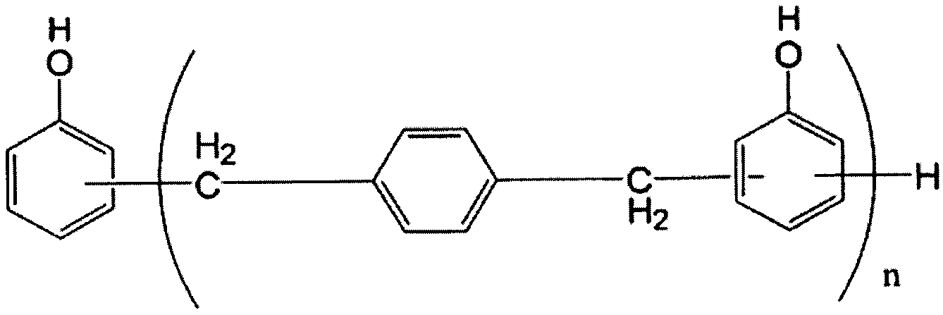
이미다졸류로는, 공지된 것을 사용할 수 있으며, 예를 들어, 2-운데실이미다졸, 2-헵타데실이미다졸, 2-에틸-4-메틸이미다졸, 2-페닐-4-메틸이미다졸, 1-시아노에틸-2-운데실이미다졸, 1-시아노에틸-2-에틸-4-메틸이미다졸, 1-시아노에틸-2-페닐이미다졸, 2-페닐-4,5-디하이드록시메틸이미다졸, 2-페닐-4-메틸-5-하이드록시메틸이미다졸 등을 들 수 있고, 이들을 단독 혹은 혼합하여 사용할 수 있다.As the imidazoles, known ones can be used, for example, 2-undecylimidazole, 2-heptadecylimidazole, 2-ethyl-4-methylimidazole, Methylimidazole, 1-cyanoethyl-2-undecylimidazole, 1-cyanoethyl-2-ethyl-4-methylimidazole, -Phenyl-4, 5-dihydroxymethylimidazole, 2-phenyl-4-methyl-5-hydroxymethylimidazole, etc. These may be used alone or in combination.
또, 그 중에서도, 이하의 화학식 10 에 나타내는 구조식을 구비하는 이미다졸류를 사용하는 것이 바람직하다. 이 화학식 10 에 나타내는 구조식의 이미다졸류를 사용함으로써, 반경화 상태의 수지층의 내흡습성을 현저하게 향상시킬 수 있어, 장기 보존 안정성이 우수하다. 이미다졸류는, 에폭시 수지의 경화시에 촉매적인 작용을 실시하는 것이며, 경화 반응의 초기 단계에 있어서, 에폭시 수지의 자기 중합 반응을 일으키는 반응 개시제로서 기여하기 때문이다.Among them, it is preferable to use imidazoles having the following structural formula (10). By using the imidazoles of the structural formula (10), the moisture absorption of the resin layer in the semi-cured state can be remarkably improved, and the long-term storage stability is excellent. The imidazoles perform catalytic action upon curing of the epoxy resin and contribute to the polymerization initiator of the epoxy resin in the initial stage of the curing reaction.
[화학식 10][Chemical formula 10]

상기 아민류의 수지 경화제로는, 공지된 아민류를 사용할 수 있다. 또, 상기 아민류의 수지 경화제로는 예를 들어 전술한 폴리아민이나 방향족 폴리아민을 사용할 수 있으며, 또, 방향족 폴리아민, 폴리아미드류 및 이들을 에폭시 수지나 다가 카르복실산과 중합 혹은 축합시켜 얻어지는 아민 어덕트체의 군에서 선택된 1 종 또는 2 종 이상을 사용해도 된다. 또, 상기 아민류의 수지 경화제로는, 4,4'-디아미노디페닐렌술폰, 3,3'-디아미노디페닐렌술폰, 4,4-디아미노디페닐, 2,2-비스[4-(4-아미노페녹시)페닐]프로판 또는 비스[4-(4-아미노페녹시)페닐]술폰 중 어느 1 종 이상을 사용하는 것이 바람직하다.As the resin curing agent for the amines, known amines can be used. As the resin curing agent for the amines, there can be used, for example, the above-mentioned polyamines or aromatic polyamines, and also aromatic polyamines and polyamides, and amine adducts obtained by polymerizing or condensing them with epoxy resins or polyvalent carboxylic acids May be used alone or in combination of two or more. Examples of the resin curing agent for the amines include 4,4'-diaminodiphenylene sulfone, 3,3'-diaminodiphenylene sulfone, 4,4-diaminodiphenyl, 2,2-bis [4 - (4-aminophenoxy) phenyl] propane or bis [4- (4-aminophenoxy) phenyl] sulfone.
상기 수지층은 경화 촉진제를 포함해도 된다. 경화 촉진제로는 공지된 경화 촉진제를 사용할 수 있다. 예를 들어, 경화 촉진제로는, 3 급 아민, 이미다졸, 우레아계 경화 촉진제 등을 사용할 수 있다.The resin layer may contain a curing accelerator. As the curing accelerator, known curing accelerators may be used. As the curing accelerator, for example, tertiary amines, imidazoles, urea curing accelerators and the like can be used.
상기 수지층은 반응 촉매를 포함해도 된다. 반응 촉매로는 공지된 반응 촉매를 사용할 수 있다. 예를 들어 반응 촉매로서 미분쇄 실리카, 3산화안티몬 등을 사용할 수 있다.The resin layer may include a reaction catalyst. As the reaction catalyst, a known reaction catalyst may be used. For example, fine particles of silica, antimony trioxide or the like can be used as a reaction catalyst.
상기 다가 카르복실산의 무수물은 에폭시 수지의 경화제로서 기여하는 성분인 것이 바람직하다. 또, 상기 다가 카르복실산의 무수물은, 무수 프탈산, 무수 말레산, 무수 트리멜리트산, 무수 피로멜리트산, 테트라하이드록시 무수 프탈산, 헥사하이드록시 무수 프탈산, 메틸헥사하이드록시 무수 프탈산, 나딘산, 메틸나딘산인 것이 바람직하다.The anhydride of the polyvalent carboxylic acid is preferably a component contributing as a curing agent for the epoxy resin. The anhydride of the polyvalent carboxylic acid may be at least one selected from phthalic anhydride, maleic anhydride, trimellitic anhydride, pyromellitic anhydride, tetrahydroxyphthalic anhydride, hexahydroxyphthalic anhydride, methylhexahydroxyphthalic anhydride, Methylnadic acid is preferable.
상기 열가소성 수지는 에폭시 수지와 중합 가능한 알코올성 수산기 이외의 관능기를 갖는 열가소성 수지여도 된다.The thermoplastic resin may be a thermoplastic resin having a functional group other than the alcoholic hydroxyl group polymerizable with the epoxy resin.
상기 폴리비닐아세탈 수지는 산기 및 수산기 이외의 에폭시 수지 또는 말레이미드 화합물과 중합 가능한 관능기를 가져도 된다. 또, 상기 폴리비닐아세탈 수지는 그 분자 내에 카르복실기, 아미노기 또는 불포화 이중 결합을 도입한 것이어도 된다.The polyvinyl acetal resin may have a functional group polymerizable with an epoxy resin or a maleimide compound other than an acid group and a hydroxyl group. In addition, the polyvinyl acetal resin may be obtained by introducing a carboxyl group, an amino group or an unsaturated double bond into the molecule.
상기 방향족 폴리아미드 수지 폴리머로는, 방향족 폴리아미드 수지와 고무성 수지를 반응시켜 얻어지는 것을 들 수 있다. 여기서, 방향족 폴리아미드 수지란, 방향족 디아민과 디카르복실산의 축중합에 의해 합성되는 것이다. 이 때의 방향족 디아민에는, 4,4'-디아미노디페닐메탄, 3,3'-디아미노디페닐술폰, m-자일렌디아민, 3,3'-옥시디아닐린 등을 사용한다. 그리고, 디카르복실산에는, 프탈산, 이소프탈산, 테레프탈산, 푸마르산 등을 사용한다.Examples of the aromatic polyamide resin polymer include those obtained by reacting an aromatic polyamide resin with a rubbery resin. Here, the aromatic polyamide resin is synthesized by condensation polymerization of an aromatic diamine and a dicarboxylic acid. As the aromatic diamine at this time, 4,4'-diaminodiphenylmethane, 3,3'-diaminodiphenylsulfone, m-xylene diamine, 3,3'-oxydianiline and the like are used. As the dicarboxylic acid, phthalic acid, isophthalic acid, terephthalic acid, fumaric acid and the like are used.
상기 방향족 폴리아미드 수지와 반응시키는 상기 고무성 수지란, 공지된 고무성 수지 또는 전술한 고무성 수지를 사용할 수 있다.The rubbery resin to be reacted with the aromatic polyamide resin may be a known rubbery resin or the aforementioned rubbery resin.
이 방향족 폴리아미드 수지 폴리머는, 구리 피복 적층판에 가공한 후의 동박을 에칭 가공할 때에, 에칭액에 의해 언더 에칭에 의한 손상을 받지 않는 것을 목적으로 사용한 것이다.This aromatic polyamide resin polymer is used for the purpose of not subjecting to damage by under etching by an etching liquid when the copper foil after being processed into the copper clad laminate is etched.
또, 상기 수지층은 동박측 (즉 캐리어 부착 동박의 극박 구리층측) 으로부터 순서로 경화 수지층 (「경화 수지층」 이란, 경화가 끝난 수지층을 의미하는 것으로 한다) 과 반경화 수지층을 순차 형성한 수지층이어도 된다. 상기 경화 수지층은, 열팽창 계수가 0 ppm/℃ ∼ 25 ppm/℃ 인 폴리이미드 수지, 폴리아미드이미드 수지, 이들의 복합 수지 중 어느 것의 수지 성분으로 구성되어도 된다.The resin layer is formed by sequentially laminating a cured resin layer (the term "cured resin layer" means a cured resin layer) and a cured resin layer in this order from the copper foil side (ie, the ultra-thin copper layer side of the copper foil with a carrier) Or a resin layer formed thereon. The cured resin layer may be composed of a resin component of any of a polyimide resin, a polyamide-imide resin, and a composite resin thereof having a thermal expansion coefficient of 0 ppm / ° C to 25 ppm / ° C.
또, 상기 경화 수지층 상에, 경화한 후의 열팽창 계수가 0 ppm/℃ ∼ 50 ppm/℃ 인 반경화 수지층을 형성해도 된다. 또, 상기 경화 수지층과 상기 반경화 수지층이 경화한 후의 수지층 전체의 열팽창 계수가 40 ppm/℃ 이하여도 된다. 상기 경화 수지층은, 유리 전이 온도가 300 ℃ 이상이어도 된다. 또, 상기 반경화 수지층은, 말레이미드계 수지 또는 방향족 말레이미드 수지를 사용하여 형성한 것이어도 된다. 상기 반경화 수지층을 형성하기 위한 수지 조성물은, 말레이미드계 수지, 에폭시 수지, 가교 가능한 관능기를 갖는 선상 폴리머를 포함하는 것이 바람직하다. 에폭시 수지는 공지된 에폭시 수지 또는 본 명세서에 기재된 에폭시 수지를 사용할 수 있다. 또, 말레이미드계 수지, 방향족 말레이미드 수지, 가교 가능한 관능기를 갖는 선상 폴리머로는, 공지된 말레이미드계 수지, 방향족 말레이미드 수지, 가교 가능한 관능기를 갖는 선상 폴리머 또는 전술한 말레이미드계 수지, 방향족 말레이미드 수지, 가교 가능한 관능기를 갖는 선상 폴리머를 사용할 수 있다.A semi-cured resin layer having a thermal expansion coefficient of 0 ppm / ° C to 50 ppm / ° C after curing may be formed on the cured resin layer. The thermal expansion coefficient of the entire resin layer after curing of the cured resin layer and the semi-cured resin layer may be 40 ppm / 占 폚 or less. The cured resin layer may have a glass transition temperature of 300 캜 or higher. The semi-cured resin layer may be formed using a maleimide resin or an aromatic maleimide resin. The resin composition for forming the semi-cured resin layer preferably includes a maleimide resin, an epoxy resin, and a linear polymer having a crosslinkable functional group. The epoxy resin may be a known epoxy resin or the epoxy resin described in this specification. Examples of the maleimide resin, the aromatic maleimide resin, and the linear polymer having a crosslinkable functional group include known maleimide resins, aromatic maleimide resins, linear polymers having a crosslinkable functional group, or the aforementioned maleimide resins, aromatic A maleimide resin, and a linear polymer having a crosslinkable functional group can be used.
또, 입체 성형 프린트 배선판 제조 용도에 적합한, 수지층을 갖는 캐리어 부착 동박을 제공하는 경우, 상기 경화 수지층은 경화한 가요성을 갖는 고분자 폴리머층인 것이 바람직하다. 상기 고분자 폴리머층은, 땜납 실장 공정에 견딜 수 있도록 150 ℃ 이상의 유리 전이 온도를 갖는 수지로 이루어지는 것이 적합하다. 상기 고분자 폴리머층은, 폴리아미드 수지, 폴리에테르술폰 수지, 아라미드 수지, 페녹시 수지, 폴리이미드 수지, 폴리비닐아세탈 수지, 폴리아미드이미드 수지 중 어느 1 종 또는 2 종 이상의 혼합 수지로 이루어지는 것이 바람직하다. 또, 상기 고분자 폴리머층의 두께는 3 ㎛ ∼ 10 ㎛ 인 것이 바람직하다.In the case of providing a copper foil with a carrier having a resin layer, which is suitable for use in the production of a molded molded printed circuit board, it is preferable that the cured resin layer is a hardened polymeric polymer layer having flexibility. The polymer polymer layer is preferably made of a resin having a glass transition temperature of 150 DEG C or more so as to withstand the solder packaging step. The polymer polymer layer is preferably composed of a mixed resin of at least one of a polyamide resin, a polyether sulfone resin, an aramid resin, a phenoxy resin, a polyimide resin, a polyvinyl acetal resin and a polyamideimide resin . It is preferable that the thickness of the polymer polymer layer is 3 mu m to 10 mu m.
또, 상기 고분자 폴리머층은, 에폭시 수지, 말레이미드계 수지, 페놀 수지, 우레탄 수지 중 어느 1 종 또는 2 종 이상을 포함하는 것이 바람직하다. 또, 상기 반경화 수지층은 두께가 10 ㎛ ∼ 50 ㎛ 인 에폭시 수지 조성물로 구성되어 있는 것이 바람직하다.It is preferable that the polymer polymer layer contains at least one of epoxy resin, maleimide resin, phenol resin and urethane resin. The semi-cured resin layer is preferably composed of an epoxy resin composition having a thickness of 10 mu m to 50 mu m.
또, 상기 에폭시 수지 조성물은 이하의 A 성분 ∼ E 성분의 각 성분을 포함하는 것인 것이 바람직하다.It is preferable that the epoxy resin composition contains the following components A to E, respectively.
A 성분:에폭시 당량이 200 이하이고, 실온에서 액상의 비스페놀 A 형 에폭시 수지, 비스페놀 F 형 에폭시 수지, 비스페놀 AD 형 에폭시 수지의 군에서 선택되는 1 종 또는 2 종 이상으로 이루어지는 에폭시 수지.Component A: an epoxy resin comprising at least one epoxy group selected from the group consisting of bisphenol A type epoxy resin, bisphenol F type epoxy resin and bisphenol AD type epoxy resin having an epoxy equivalent of 200 or less and being liquid at room temperature.
B 성분:고내열성 에폭시 수지.Component B: High heat resistant epoxy resin.
C 성분:인 함유 에폭시계 수지, 포스파젠계 수지 중 어느 1 종 또는 이들을 혼합한 수지인 인 함유 난연성 수지.Component C: phosphorus-containing flame retardant resin which is a resin obtained by mixing any one of phosphorus-containing epoxy resin and phosphazene resin or a mixture thereof.
D 성분:비점이 50 ℃ ∼ 200 ℃ 의 범위에 있는 용제에 가용인 성질을 구비하는 액상 고무 성분으로 변성한 고무 변성 폴리아미드이미드 수지.Component D: a rubber-modified polyamide-imide resin modified with a liquid rubber component having properties soluble in a solvent having a boiling point in the range of 50 to 200 ° C.
E 성분:수지 경화제.Component E: Resin curing agent.
B 성분은, 소위 유리 전이점 Tg 가 높은 「고내열성 에폭시 수지」 이다. 여기서 말하는 「고내열성 에폭시 수지」 는, 노볼락형 에폭시 수지, 크레졸 노볼락형 에폭시 수지, 페놀 노볼락형 에폭시 수지, 나프탈렌형 에폭시 수지 등의 다관능 에폭시 수지인 것이 바람직하다.The component B is a " high heat resistant epoxy resin " having a so-called glass transition point Tg. The "heat-resistant epoxy resin" referred to herein is preferably a polyfunctional epoxy resin such as novolak type epoxy resin, cresol novolak type epoxy resin, phenol novolak type epoxy resin, and naphthalene type epoxy resin.
C 성분의 인 함유 에폭시 수지로서, 전술한 인 함유 에폭시 수지를 사용할 수 있다. 또, C 성분의 포스파젠계 수지로서, 전술한 포스파젠계 수지를 사용할 수 있다.As the phosphorus-containing epoxy resin of component C, the above-mentioned phosphorus-containing epoxy resin can be used. As the C-component phosphazene-based resin, the above-mentioned phosphazene-based resin can be used.
D 성분의 고무 변성 폴리아미드이미드 수지로서, 전술한 고무 변성 폴리아미드이미드 수지를 사용할 수 있다. E 성분의 수지 경화제로서, 전술한 수지 경화제를 사용할 수 있다.As the rubber-modified polyamide-imide resin of component D, the above-mentioned rubber-modified polyamide-imide resin can be used. As the resin curing agent for the component E, the aforementioned resin curing agent can be used.
이상에 나타낸 수지 조성물에 용제를 첨가하여 수지 바니시로서 사용하고, 프린트 배선판의 접착층으로서 열 경화성 수지층을 형성한다. 당해 수지 바니시는, 상기 서술한 수지 조성물에 용제를 첨가하여, 수지 고형분량이 30 wt% ∼ 70 wt% 인 범위로 조제하고, MIL 규격에 있어서의 MIL-P-13949G 에 준거하여 측정했을 때의 레진 플로우가 5 % ∼ 35 % 의 범위에 있는 반경화 수지막의 형성이 가능하다. 용제에는, 공지된 용제 또는 전술한 용제를 사용할 수 있다.A solvent is added to the resin composition as described above and used as a resin varnish to form a thermosetting resin layer as an adhesive layer of a printed wiring board. The resin varnish is prepared by adding a solvent to the above-mentioned resin composition to prepare a resin having a solid content of 30 wt% to 70 wt% and measuring the resin as measured according to MIL-P-13949G in MIL specification It is possible to form a semi-cured resin film having a flow in the range of 5% to 35%. For the solvent, a known solvent or the above-mentioned solvent may be used.
상기 수지층은 동박측으로부터 순서로 제 1 열 경화성 수지층과, 당해 제 1 열 경화성 수지층의 표면에 위치하는 제 2 열 경화성 수지층을 갖는 수지층으로서, 제 1 열 경화성 수지층은, 배선판 제조 프로세스에 있어서의 디스미어 처리시의 약품에 용해하지 않는 수지 성분으로 형성된 것이며, 제 2 열 경화성 수지층은, 배선판 제조 프로세스에 있어서의 디스미어 처리시의 약품에 용해하고 세정 제거 가능한 수지를 사용하여 형성한 것이어도 된다. 상기 제 1 열 경화성 수지층은, 폴리이미드 수지, 폴리에테르술폰, 폴리페닐렌옥사이드 중 어느 1 종 또는 2 종 이상을 혼합한 수지 성분을 사용하여 형성한 것이어도 된다. 상기 제 2 열 경화성 수지층은, 에폭시 수지 성분을 사용하여 형성한 것이어도 된다. 상기 제 1 열 경화성 수지층의 두께 t1 (㎛) 는, 캐리어 부착 동박의 조화면 조도를 Rz (㎛) 로 하고, 제 2 열 경화성 수지층의 두께를 t2 (㎛) 로 했을 때, t1 은 Rz < t1 < t2 의 조건을 만족하는 두께인 것이 바람직하다.Wherein the resin layer is a resin layer having a first thermosetting resin layer sequentially from the copper foil side and a second thermosetting resin layer positioned on the surface of the first thermosetting resin layer, And the second thermosetting resin layer is formed of a resin component which is dissolved in a drug used in the desmear treatment in the process of producing a wiring board and is made of a resin that can be cleaned and removed Or the like. The first thermosetting resin layer may be formed using a resin component in which one or more of polyimide resin, polyethersulfone, and polyphenylene oxide are mixed. The second thermosetting resin layer may be formed using an epoxy resin component. The thickness t1 (占 퐉) of the first thermosetting resin layer is represented by Rz (占 퐉) and the thickness of the second thermosetting resin layer is t2 (占 퐉) It is preferable that the thickness satisfies the condition of < t1 < t2.
상기 수지층은 골격재에 수지를 함침시킨 프리프레그여도 된다. 상기 골격재에 함침시킨 수지는 열 경화성 수지인 것이 바람직하다. 상기 프리프레그는 공지된 프리프레그 또는 프린트 배선판 제조에 사용하는 프리프레그여도 된다.The resin layer may be a prepreg impregnated with a resin in a skeletal material. The resin impregnated in the skeleton is preferably a thermosetting resin. The prepreg may be a known prepreg or a prepreg used for manufacturing a printed wiring board.
상기 골격재는 아라미드 섬유 또는 유리 섬유 또는 전체 방향족 폴리에스테르 섬유를 포함해도 된다. 상기 골격재는 아라미드 섬유 또는 유리 섬유 또는 전체 방향족 폴리에스테르 섬유의 부직포 혹은 직포인 것이 바람직하다. 또, 상기 전체 방향족 폴리에스테르 섬유는 융점이 300 ℃ 이상인 전체 방향족 폴리에스테르 섬유인 것이 바람직하다. 상기 융점이 300 ℃ 이상인 전체 방향족 폴리에스테르 섬유란, 소위 액정 폴리머라고 칭해지는 수지를 사용하여 제조되는 섬유이며, 당해 액정 폴리머는 2-하이드록실-6-나프토산 및 p-하이드록시벤조산의 중합체를 주성분으로 하는 것이다. 이 전체 방향족 폴리에스테르 섬유는, 저유전율, 낮은 유전 정접을 갖기 때문에, 전기적 절연층의 구성재로서 우수한 성능을 가지며, 유리 섬유 및 아라미드 섬유와 마찬가지로 사용하는 것이 가능한 것이다.The skeletal material may comprise aramid fibers or glass fibers or wholly aromatic polyester fibers. The skeleton material is preferably a nonwoven fabric or woven fabric of aramid fiber, glass fiber, or all aromatic polyester fiber. The total aromatic polyester fiber is preferably a wholly aromatic polyester fiber having a melting point of 300 캜 or higher. The above all-aromatic polyester fiber having a melting point of 300 ° C or higher is a fiber produced by using a resin called a liquid crystal polymer. The liquid crystal polymer is a polymer of 2-hydroxyl-6-naphthoic acid and p-hydroxybenzoic acid It is the main component. This whole aromatic polyester fiber has a low dielectric constant and a low dielectric loss tangent, and therefore has excellent performance as a constituent material of the electrically insulating layer and can be used in the same manner as glass fibers and aramid fibers.
또한, 상기 부직포 및 직포를 구성하는 섬유는, 그 표면의 수지와의 젖음성을 향상시키기 위해서, 실란 커플링제 처리를 실시하는 것이 바람직하다. 이 때의 실란 커플링제는, 사용 목적에 따라 공지된 아미노계, 에폭시계 등의 실란 커플링제 또는 전술한 실란 커플링제를 사용할 수 있다.The fibers constituting the nonwoven fabric and the woven fabric are preferably subjected to a silane coupling agent treatment in order to improve the wettability of the surface of the nonwoven fabric and the woven fabric with the resin. As the silane coupling agent at this time, there may be used known silane coupling agents such as amino and epoxy coupling agents or silane coupling agents described above depending on the purpose of use.
또, 상기 프리프레그는 공칭 두께가 70 ㎛ 이하인 아라미드 섬유 또는 유리 섬유를 사용한 부직포, 혹은, 공칭 두께가 30 ㎛ 이하인 유리 크로스로 이루어지는 골격재에 열 경화성 수지를 함침시킨 프리프레그여도 된다.The prepreg may be a nonwoven fabric using aramid fibers or glass fibers having a nominal thickness of 70 μm or less or a prepreg obtained by impregnating a skeletal material made of a glass cloth having a nominal thickness of 30 μm or less with a thermosetting resin.
(수지층이 유전체 (유전체 필러) 를 포함하는 경우) (When the resin layer includes a dielectric (dielectric filler)
상기 수지층은 유전체 (유전체 필러) 를 포함해도 된다.The resin layer may include a dielectric (dielectric filler).
상기 어느 것의 수지층 또는 수지 조성물에 유전체 (유전체 필러) 를 포함시키는 경우에는, 캐패시터층을 형성하는 용도에 사용하여, 캐패시터 회로의 전기 용량을 증대시킬 수 있는 것이다. 이 유전체 (유전체 필러) 에는, BaTiO3, SrTiO3, Pb(Zr-Ti)O3 (통칭 PZT), PbLaTiO3·PbLaZrO (통칭 PLZT), SrBi2Ta2O9 (통칭 SBT) 등의 페브로스카이트 구조를 갖는 복합 산화물의 유전체 분말을 사용한다.When a dielectric (dielectric filler) is included in any of the above resin layers or resin compositions, it can be used for forming a capacitor layer, thereby increasing the capacitance of the capacitor circuit. The dielectric material (dielectric filler) includes a ferroelectric material such as BaTiO 3 , SrTiO 3 , Pb (Zr-Ti) O 3 (commonly referred to as PZT), PbLaTiO 3 .PbLaZrO (commonly referred to as PLZT), and SrBi 2 Ta 2 O 9 A dielectric powder of a composite oxide having a kite structure is used.
유전체 (유전체 필러) 는 분상 (粉狀) 이어도 된다. 유전체 (유전체 필러) 가 분상인 경우, 이 유전체 (유전체 필러) 의 분체 특성은, 먼저 입경이 0.01 ㎛ ∼ 3.0 ㎛, 바람직하게는 0.02 ㎛ ∼ 2.0 ㎛ 의 범위인 것일 필요가 있다. 여기서 말하는 입경은, 분립끼리가 어느 일정한 2 차 응집 상태를 형성하고 있기 때문에, 레이저 회절 산란식 입도 분포 측정법이나 BET 법 등의 측정값으로부터 평균 입경을 추측하는 간접 측정에서는 정밀도가 떨어지는 것이 되기 때문에 사용할 수 없고, 유전체 (유전체 필러) 를 주사형 전자 현미경 (SEM) 으로 직접 관찰하여, 그 SEM 이미지를 화상 해석하여 얻어지는 평균 입경을 말하는 것이다. 본건 명세서에서는 이 때의 입경을 DIA 라고 표시하고 있다. 또한, 본건 명세서에 있어서의 주사형 전자 현미경 (SEM) 을 사용하여 관찰되는 유전체 (유전체 필러) 의 분체의 화상 해석은, 아사히 엔지니어링 주식회사 제조의 IP-1000PC 를 사용하여, 원도 (圓度) 임계값 10, 겹침도 20 으로 하여 원형 입자 해석을 실시하고, 평균 입경 DIA 를 구한 것이다.The dielectric (dielectric filler) may be in powder form. When the dielectric (dielectric filler) is in the form of powder, it is necessary that the particle size of the dielectric (dielectric filler) is firstly in the range of 0.01 탆 to 3.0 탆, preferably 0.02 탆 to 2.0 탆. Since the particle diameters referred to herein form a certain degree of secondary agglomeration among the granules, the precision is inferior in the indirect measurement in which the average particle diameter is estimated from the measurement values such as the laser diffraction scattering type particle size distribution measurement method and the BET method, And refers to an average particle size obtained by directly observing a dielectric (dielectric filler) with a scanning electron microscope (SEM) and analyzing the SEM image. In this specification, the particle size at this time is denoted by DIA. The image analysis of the powder of the dielectric (dielectric filler) observed using a scanning electron microscope (SEM) in the present specification was carried out using IP-1000PC manufactured by Asahi Engineering Co., Ltd., A value of 10 and an overlapping degree of 20, and the average particle diameter DIA was obtained.
상기 서술한 실시형태에 의해, 당해 내층 코어재의 내층 회로 표면과 유전체를 포함하는 수지층의 밀착성을 향상시키고, 낮은 유전 정접을 구비하는 캐패시터 회로층을 형성하기 위한 유전체를 포함하는 수지층을 갖는 캐리어 부착 동박을 제공할 수 있다.According to the above-described embodiment, a carrier having a resin layer including a dielectric for improving the adhesion between the inner layer circuit surface of the inner layer core material and the resin layer including the dielectric and for forming the capacitor circuit layer having low dielectric tangent It is possible to provide an attached copper foil.
전술한 수지층에 포함되는 수지 및/또는 수지 조성물 및/또는 화합물을 예를 들어 메틸에틸케톤 (MEK), 시클로펜타논, 디메틸포름아미드, 디메틸아세트아미드, N-메틸피롤리돈, 톨루엔, 메탄올, 에탄올, 프로필렌글리콜모노메틸에테르, 디메틸포름아미드, 디메틸아세트아미드, 시클로헥사논, 에틸셀로솔브, N-메틸-2-피롤리돈, N,N-디메틸아세트아미드, N,N-디메틸포름아미드 등의 용제에 용해하여 수지액 (수지 바니시) 으로 하고, 이것을 상기 극박 구리층 상, 혹은 상기 내열층, 방청층, 혹은 상기 크로메이트 처리층, 혹은 상기 실란 커플링제층 상에, 예를 들어 롤 코터법 등에 의해 도포하고, 이어서 필요에 따라 가열 건조시켜 용제를 제거하여 B 스테이지 상태로 한다. 건조에는 예를 들어 열풍 건조로를 사용하면 되고, 건조 온도는 100 ∼ 250 ℃, 바람직하게는 130 ∼ 200 ℃ 이면 된다. 상기 수지층의 조성물을 용제를 사용하여 용해하고, 수지 고형분 3 wt% ∼ 70 wt%, 바람직하게는, 3 wt% ∼ 60 wt%, 바람직하게는 10 wt% ∼ 40 wt%, 보다 바람직하게는 25 wt% ∼ 40 wt% 의 수지액으로 해도 된다. 또한, 메틸에틸케톤과 시클로펜타논의 혼합 용제를 사용하여 용해하는 것이, 환경적인 견지에서 현단계에서는 가장 바람직하다. 또한, 용제에는 비점이 50 ℃ ∼ 200 ℃ 의 범위인 용제를 사용하는 것이 바람직하다.The resin and / or the resin composition and / or the compound contained in the resin layer described above may be dissolved in a solvent such as methyl ethyl ketone (MEK), cyclopentanone, dimethylformamide, dimethylacetamide, N-methylpyrrolidone, , Ethanol, propylene glycol monomethyl ether, dimethyl formamide, dimethylacetamide, cyclohexanone, ethyl cellosolve, N-methyl-2-pyrrolidone, N, N-dimethylacetamide, N, (Resin varnish) by dissolving it in a solvent such as an amide or the like to form a resin solution (resin varnish) on the extremely thin copper layer or the heat resistant layer, the rust prevention layer, or the chromate treatment layer or the silane coupling agent layer, Coater method or the like, and then, if necessary, heated and dried to remove the solvent to obtain a B-stage state. For drying, for example, a hot-air drying furnace may be used, and the drying temperature may be 100 to 250 ° C, preferably 130 to 200 ° C. The composition of the resin layer is dissolved by using a solvent, and the resin solid content is 3 wt% to 70 wt%, preferably 3 wt% to 60 wt%, preferably 10 wt% to 40 wt%, more preferably, 25 wt% to 40 wt% resin solution may be used. Further, it is most preferable to dissolve using a mixed solvent of methyl ethyl ketone and cyclopentanone from the environmental viewpoint at the present stage. It is preferable to use a solvent having a boiling point in the range of 50 ° C to 200 ° C.
또, 상기 수지층은 MIL 규격에 있어서의 MIL-P-13949G 에 준거하여 측정했을 때의 레진 플로우가 5 % ∼ 35 % 의 범위에 있는 반경화 수지막인 것이 바람직하다.It is preferable that the resin layer is a semi-cured resin film having a resin flow in a range of 5% to 35% when measured according to MIL-P-13949G in the MIL standard.
본건 명세서에 있어서, 레진 플로우란, MIL 규격에 있어서의 MIL-P-13949G 에 준거하여, 수지 두께를 55 ㎛ 로 한 수지 부착 동박으로부터 가로세로 10 ㎝ 시료를 4 매 샘플링하고, 이 4 매의 시료를 겹친 상태 (적층체) 로 프레스 온도 171 ℃, 프레스압 14 kgf/㎠, 프레스 시간 10 분의 조건으로 접합하고, 그 때의 수지 유출 중량을 측정한 결과로부터 수학식 1 에 기초하여 산출한 값이다.In the present specification, the resin flow is a method in which four samples of 10 cm in length and 10 cm length are sampled from a resin-coated copper foil having a resin thickness of 55 탆 in accordance with MIL-P-13949G in the MIL standard, At a press temperature of 171 DEG C, a press pressure of 14 kgf / cm < 2 >, and a press time of 10 minutes, and the value calculated based on the formula (1) from the result of measuring the resin outflow weight at that time to be.

상기 수지층을 구비한 캐리어 부착 동박 (수지가 부착된 캐리어 부착 동박) 은, 그 수지층을 기재에 중첩한 후 전체를 열 압착하여 그 수지층을 열 경화시키고, 이어서 캐리어를 박리하여 극박 구리층을 표출시키고 (당연히 표출하는 것은 그 극박 구리층의 중간층측의 표면이다), 거기에 소정의 배선 패턴을 형성한다는 양태로 사용된다.The resin-coated copper foil with the resin layer (resin-coated copper foil with a carrier) having the resin layer is superimposed on the base material and then thermally pressed to thermally cure the resin layer. Subsequently, the carrier is peeled, (Of course, the surface to be exposed is the surface of the intermediate layer side of the extremely thin copper layer), and is used as an embodiment of forming a predetermined wiring pattern there.
이 수지가 부착된 캐리어 부착 동박을 사용하면, 다층 프린트 배선 기판의 제조시에 있어서의 프리프레그재의 사용 매수를 줄일 수 있다. 게다가, 수지층의 두께를 층간 절연을 확보할 수 있는 두께로 하거나, 프리프레그재를 전혀 사용하지 않아도 구리 피복 적층판을 제조할 수 있다. 또 이 때, 기재의 표면에 절연 수지를 언더코트하여 표면의 평활성을 더욱 개선할 수도 있다.The use of the copper foil with a carrier to which the resin is adhered can reduce the number of prepreg materials used in manufacturing a multilayer printed wiring board. Furthermore, the thickness of the resin layer can be set to a sufficient thickness to ensure interlayer insulation, or a copper clad laminate can be manufactured without using any prepreg material. At this time, the surface of the substrate may be undercoated with an insulating resin to further improve the smoothness of the surface.
또한, 프리프레그재를 사용하지 않는 경우에는, 프리프레그재의 재료 코스트가 절약되고, 또 적층 공정도 간략해지므로 경제적으로 유리해지고, 게다가, 프리프레그재의 두께분만큼 제조되는 다층 프린트 배선 기판의 두께는 얇아져, 1 층의 두께가 100 ㎛ 이하인 극박의 다층 프린트 배선 기판을 제조할 수 있다는 이점이 있다.In addition, when the prepreg material is not used, the material cost of the prepreg material is reduced, and the lamination step is simplified, which is economically advantageous. Further, the thickness of the multilayer printed wiring board manufactured by the thickness of the prepreg material is It is possible to produce an ultra-thin multilayer printed circuit board having a thickness of 100 m or less in one layer.
이 수지층의 두께는 0.1 ∼ 120 ㎛ 인 것이 바람직하다.The thickness of the resin layer is preferably 0.1 to 120 탆.
수지층의 두께가 0.1 ㎛ 보다 얇아지면, 접착력이 저하되고, 프리프레그재를 개재시키는 일 없이 이 수지가 부착된 캐리어 부착 동박을 내층재를 구비한 기재에 적층했을 때에, 내층재의 회로 사이의 층간 절연을 확보하는 것이 곤란해지는 경우가 있다. 한편, 수지층의 두께를 120 ㎛ 보다 두껍게 하면, 1 회의 도포 공정으로 목적 두께의 수지층을 형성하는 것이 곤란해지고, 여분의 재료비와 공정수가 들기 때문에 경제적으로 불리해지는 경우가 있다.When the thickness of the resin layer is smaller than 0.1 占 퐉, the adhesive force is lowered, and when the copper foil with a carrier on which the resin is adhered is laminated on a base material provided with the inner layer material without interposing the prepreg material, It may be difficult to secure a certain amount of time. On the other hand, if the thickness of the resin layer is made larger than 120 占 퐉, it is difficult to form the resin layer having the desired thickness in one coating step, resulting in economical disadvantage because extra material cost and number of steps are involved.
또한, 수지층을 갖는 캐리어 부착 동박이 극박의 다층 프린트 배선판을 제조하는 것에 사용되는 경우에는, 상기 수지층의 두께를 0.1 ㎛ ∼ 5 ㎛, 보다 바람직하게는 0.5 ㎛ ∼ 5 ㎛, 보다 바람직하게는 1 ㎛ ∼ 5 ㎛로 하는 것이, 다층 프린트 배선판의 두께를 작게 하기 위해서 바람직하다.When the copper foil with a carrier having a resin layer is used for producing an ultra-thin multilayered printed circuit board, the thickness of the resin layer is preferably 0.1 to 5 mu m, more preferably 0.5 to 5 mu m, It is preferable that the thickness is 1 占 퐉 to 5 占 퐉 in order to reduce the thickness of the multilayer printed wiring board.
또, 수지층이 유전체를 포함하는 경우에는, 수지층의 두께는 0.1 ∼ 50 ㎛ 인 것이 바람직하고, 0.5 ㎛ ∼ 25 ㎛ 인 것이 바람직하며, 1.0 ㎛ ∼ 15 ㎛ 인 것이 보다 바람직하다.When the resin layer contains a dielectric, the thickness of the resin layer is preferably 0.1 to 50 탆, more preferably 0.5 to 25 탆, and more preferably 1.0 to 15 탆.
또, 상기 경화 수지층, 반경화 수지층과의 총 수지 층두께는 0.1 ㎛ ∼ 120 ㎛ 인 것이 바람직하고, 5 ㎛ ∼ 120 ㎛ 인 것이 바람직하고, 10 ㎛ ∼ 120 ㎛ 인 것이 바람직하며, 10 ㎛ ∼ 60 ㎛ 의 것이 보다 바람직하다. 그리고, 경화 수지층의 두께는 2 ㎛ ∼ 30 ㎛ 인 것이 바람직하고, 3 ㎛ ∼ 30 ㎛ 인 것이 바람직하며, 5 ∼ 20 ㎛ 인 것이 보다 바람직하다. 또, 반경화 수지층의 두께는 3 ㎛ ∼ 55 ㎛ 인 것이 바람직하고, 7 ㎛ ∼ 55 ㎛ 인 것이 바람직하며, 15 ∼ 115 ㎛ 인 것이 보다 바람직하다. 총 수지층 두께가 120 ㎛ 를 초과하면, 얇은 두께의 다층 프린트 배선판을 제조하는 것이 어려워지는 경우가 있고, 5 ㎛ 미만에서는 얇은 두께의 다층 프린트 배선판을 형성하기 쉬워지기는 하지만, 내층의 회로간에 있어서의 절연층인 수지층이 지나치게 얇아져, 내층의 회로간의 절연성을 불안정하게 하는 경향이 발생하는 경우가 있기 때문이다. 또, 경화 수지층 두께가 2 ㎛ 미만이면, 동박 조화면의 표면 조도를 고려할 필요가 발생하는 경우가 있다. 반대로 경화 수지층 두께가 20 ㎛ 를 초과하면, 경화가 끝난 수지층에 의한 효과는 특별히 향상되는 일이 없어지는 경우가 있어, 총 절연층 두께는 두꺼워진다.The thickness of the total resin layer with respect to the cured resin layer and the semi-cured resin layer is preferably 0.1 mu m to 120 mu m, more preferably 5 mu m to 120 mu m, more preferably 10 mu m to 120 mu m, And more preferably from 60 to 60 mu m. The thickness of the cured resin layer is preferably 2 to 30 탆, more preferably 3 to 30 탆, and more preferably 5 to 20 탆. The thickness of the semi-cured resin layer is preferably in the range of 3 탆 to 55 탆, more preferably in the range of 7 탆 to 55 탆, and more preferably in the range of 15 탆 to 115 탆. If the thickness of the total resin layer exceeds 120 탆, it may be difficult to produce a multilayer printed wiring board having a thin thickness. If the total resin layer thickness is less than 5 탆, it is easy to form a multilayer printed wiring board having a thin thickness. However, The resin layer which is the insulating layer of the inner layer becomes too thin, and there is a tendency that the insulation between the circuits of the inner layer becomes unstable. If the thickness of the cured resin layer is less than 2 占 퐉, it may be necessary to consider the surface roughness of the copper foil roughened surface. On the other hand, if the thickness of the cured resin layer exceeds 20 占 퐉, the effect of the cured resin layer may not be particularly improved, and the total thickness of the insulating layer becomes thick.
또한, 상기 수지층의 두께를 0.1 ㎛ ∼ 5 ㎛ 로 하는 경우에는, 수지층과 캐리어 부착 동박의 밀착성을 향상시키기 위해서, 극박 구리층 상에 내열층 및/또는 방청층 및/또는 크로메이트 처리층 및/또는 실란 커플링 처리층을 형성한 후에, 당해 내열층 또는 방청층 또는 크로메이트 처리층 또는 실란 커플링 처리층 상에 수지층을 형성하는 것이 바람직하다.When the thickness of the resin layer is from 0.1 to 5 占 퐉, it is preferable that the heat-resistant layer and / or the anticorrosion layer and / or the chromate treatment layer and / or the antireflection layer are formed on the ultra-thin copper layer in order to improve the adhesion between the resin layer and the copper- It is preferable to form a resin layer on the heat resistant layer or rustproof layer, the chromate treatment layer or the silane coupling treatment layer after the silane coupling treatment layer is formed.
또한, 전술한 수지층의 두께는, 임의의 10 점에 있어서 단면 관찰에 의해 측정한 두께의 평균값을 말한다.The thickness of the resin layer mentioned above refers to an average value of the thickness measured at any 10 points by cross-sectional observation.
또한, 이 수지가 부착된 캐리어 부착 동박의 또 하나의 제품 형태로는, 상기 극박 구리층 상, 혹은 상기 내열층, 방청층, 혹은 상기 크로메이트 처리층, 혹은 상기 실란 커플링 처리층 상에 수지층으로 피복하고, 반경화 상태로 한 후, 이어서 캐리어를 박리하여, 캐리어가 존재하지 않는, 수지 부착 동박의 형태로 제조하는 것도 가능하다.Further, as another product form of the copper foil with a carrier on which the resin is adhered, it is preferable that the resin layer is formed on the extremely thin copper layer or on the heat resistant layer, rustproofing layer or the chromate treatment layer, It is possible to produce the resin in the form of a resin-coated copper foil free from carriers by peeling the carrier after it is semi-cured.
이하에, 본 발명에 관련된 캐리어 부착 동박을 사용한 프린트 배선판의 제조 공정의 예를 몇 가지 나타낸다.Hereinafter, several examples of the production process of a printed wiring board using the copper foil with a carrier according to the present invention are shown.
본 발명에 관련된 프린트 배선판의 제조 방법의 일 실시형태에 있어서는, 본 발명에 관련된 캐리어 부착 동박과 절연 기판을 준비하는 공정, 상기 캐리어 부착 동박과 절연 기판을 적층하는 공정, 상기 캐리어 부착 동박과 절연 기판을 극박 구리층측이 절연 기판과 대향하도록 적층한 후에, 상기 캐리어 부착 동박의 캐리어를 박리하는 공정을 거쳐 구리 피복 적층판을 형성하고, 그 후, 세미 애디티브법, 모디파이드 세미 애디티브법, 파틀리 애디티브법 및 서브트랙티브법 중 어느 방법에 의해 회로를 형성하는 공정을 포함한다. 절연 기판은 내층 회로가 삽입된 것으로 하는 것도 가능하다.In one embodiment of the method for manufacturing a printed wiring board according to the present invention, there is provided a method for manufacturing a printed wiring board, comprising the steps of: preparing a copper foil with a carrier and an insulating substrate according to the present invention; laminating the copper foil with a carrier and an insulating substrate; Is laminated so that the extremely thin copper layer side faces the insulating substrate and then the carrier of the copper foil with a carrier is peeled off to form a copper clad laminate. Thereafter, a semi-additive process, a modified semi-additive process, An additive method, and a subtractive method. It is also possible that the insulating substrate has an inner layer circuit inserted therein.
본 발명에 있어서, 세미 애디티브법이란, 절연 기판 또는 동박 시드층 상에 얇은 무전해 도금을 실시하고, 패턴을 형성 후, 전기 도금 및 에칭을 이용하여 도체 패턴을 형성하는 방법을 가리킨다.In the present invention, the semi-additive method refers to a method in which a thin electroless plating is performed on an insulating substrate or a copper foil seed layer to form a pattern, and then a conductive pattern is formed using electroplating and etching.
따라서, 세미 애디티브법을 이용한 본 발명에 관련된 프린트 배선판의 제조 방법의 일 실시형태에 있어서는, Therefore, in one embodiment of the method for producing a printed wiring board according to the present invention using the semi-additive method,
본 발명에 관련된 캐리어 부착 동박과 절연 기판을 준비하는 공정, A step of preparing a copper foil with a carrier and an insulating substrate according to the present invention,
상기 캐리어 부착 동박과 절연 기판을 적층하는 공정,A step of laminating the copper foil with a carrier and an insulating substrate,
상기 캐리어 부착 동박과 절연 기판을 적층한 후에, 상기 캐리어 부착 동박의 캐리어를 박리하는 공정,A step of peeling the carrier of the carrier-coated copper foil after the carrier-coated copper foil and the insulating substrate are laminated,
상기 캐리어를 박리하여 노출한 극박 구리층을 산 등의 부식 용액을 사용한 에칭이나 플라즈마 등의 방법에 의해 모두 제거하는 공정, A step of removing all of the extremely thin copper layer exposed by peeling off the carrier by a method such as etching or plasma using a corrosive solution such as an acid,
상기 극박 구리층을 에칭에 의해 제거함으로써 노출한 상기 수지에 스루홀 또는/및 블라인드 비아를 형성하는 공정, A step of forming a through hole and / or a blind via in the exposed resin by removing the extremely thin copper layer by etching,
상기 스루홀 또는/및 블라인드 비아를 포함하는 영역에 대해 디스미어 처리를 실시하는 공정,A step of performing a desmear treatment on an area including the through hole and / or the blind via,
상기 수지 및 상기 스루홀 또는/및 블라인드 비아를 포함하는 영역에 대해 무전해 도금층을 형성하는 공정, A step of forming an electroless plating layer on a region including the resin and the through hole and / or the blind via,
상기 무전해 도금층 상에 도금 레지스트를 형성하는 공정,A step of forming a plating resist on the electroless plating layer,
상기 도금 레지스트에 대해 노광하고, 그 후, 회로가 형성되는 영역의 도금 레지스트를 제거하는 공정,A step of exposing the plating resist, thereafter removing the plating resist in a region where a circuit is formed,
상기 도금 레지스트가 제거된 상기 회로가 형성되는 영역에 전해 도금층을 형성하는 공정,A step of forming an electroplating layer in a region where the plating resist is removed,
상기 도금 레지스트를 제거하는 공정,A step of removing the plating resist,
상기 회로가 형성되는 영역 이외의 영역에 있는 무전해 도금층을 플래시 에칭 등에 의해 제거하는 공정,A step of removing the electroless plating layer in a region other than the region where the circuit is formed by flash etching or the like,
을 포함한다..
세미 애디티브법을 이용한 본 발명에 관련된 프린트 배선판의 제조 방법의 다른 일 실시형태에 있어서는, In another embodiment of the method for producing a printed wiring board according to the present invention using the semi-additive method,
본 발명에 관련된 캐리어 부착 동박과 절연 기판을 준비하는 공정, A step of preparing a copper foil with a carrier and an insulating substrate according to the present invention,
상기 캐리어 부착 동박과 절연 기판을 적층하는 공정,A step of laminating the copper foil with a carrier and an insulating substrate,
상기 캐리어 부착 동박과 절연 기판을 적층한 후에, 상기 캐리어 부착 동박의 캐리어를 박리하는 공정,A step of peeling the carrier of the carrier-coated copper foil after the carrier-coated copper foil and the insulating substrate are laminated,
상기 캐리어를 박리하여 노출한 극박 구리층을 산 등의 부식 용액을 사용한 에칭이나 플라즈마 등의 방법에 의해 모두 제거하는 공정, A step of removing all of the extremely thin copper layer exposed by peeling off the carrier by a method such as etching or plasma using a corrosive solution such as an acid,
상기 극박 구리층을 에칭에 의해 제거함으로써 노출한 상기 수지의 표면에 대해 무전해 도금층을 형성하는 공정, A step of forming an electroless plating layer on the exposed surface of the resin by removing the extremely thin copper layer by etching,
상기 무전해 도금층 상에 도금 레지스트를 형성하는 공정,A step of forming a plating resist on the electroless plating layer,
상기 도금 레지스트에 대해 노광하고, 그 후, 회로가 형성되는 영역의 도금 레지스트를 제거하는 공정,A step of exposing the plating resist, thereafter removing the plating resist in a region where a circuit is formed,
상기 도금 레지스트가 제거된 상기 회로가 형성되는 영역에 전해 도금층을 형성하는 공정,A step of forming an electroplating layer in a region where the plating resist is removed,
상기 도금 레지스트를 제거하는 공정,A step of removing the plating resist,
상기 회로가 형성되는 영역 이외의 영역에 있는 무전해 도금층 및 극박 구리층을 플래시 에칭 등에 의해 제거하는 공정, A step of removing the electroless plating layer and the ultra-thin copper layer in regions other than the region where the circuit is formed by flash etching or the like,
을 포함한다..
본 발명에 있어서, 모디파이드 세미 애디티브법이란, 절연층 상에 금속박을 적층하고, 도금 레지스트에 의해 비회로 형성부를 보호하고, 전해 도금에 의해 회로 형성부의 구리 두께 형성을 실시한 후, 레지스트를 제거하고, 상기 회로 형성부 이외의 금속박을 (플래시) 에칭으로 제거함으로써, 절연층 상에 회로를 형성하는 방법을 가리킨다.In the present invention, the modified semi-additive method is a method in which a metal foil is laminated on an insulating layer, a non-circuit forming portion is protected by a plating resist, a copper thickness is formed in the circuit forming portion by electrolytic plating, And a metal foil other than the circuit forming portion is removed by (flash) etching to form a circuit on the insulating layer.
따라서, 모디파이드 세미 애디티브법을 이용한 본 발명에 관련된 프린트 배선판의 제조 방법의 일 실시형태에 있어서는, Therefore, in one embodiment of the method for producing a printed wiring board according to the present invention using a modified semi-additive method,
본 발명에 관련된 캐리어 부착 동박과 절연 기판을 준비하는 공정, A step of preparing a copper foil with a carrier and an insulating substrate according to the present invention,
상기 캐리어 부착 동박과 절연 기판을 적층하는 공정,A step of laminating the copper foil with a carrier and an insulating substrate,
상기 캐리어 부착 동박과 절연 기판을 적층한 후에, 상기 캐리어 부착 동박의 캐리어를 박리하는 공정,A step of peeling the carrier of the carrier-coated copper foil after the carrier-coated copper foil and the insulating substrate are laminated,
상기 캐리어를 박리하여 노출한 극박 구리층과 절연 기판에 스루홀 또는/및 블라인드 비아를 형성하는 공정, A step of forming a through hole and / or a blind via in the ultra-thin copper layer and the insulating substrate exposed by peeling the carrier,
상기 스루홀 또는/및 블라인드 비아를 포함하는 영역에 대해 디스미어 처리를 실시하는 공정,A step of performing a desmear treatment on an area including the through hole and / or the blind via,
상기 스루홀 또는/및 블라인드 비아를 포함하는 영역에 대해 무전해 도금층을 형성하는 공정,A step of forming an electroless plating layer on a region including the through hole and / or the blind via,
상기 캐리어를 박리하여 노출한 극박 구리층 표면에 도금 레지스트를 형성하는 공정,A step of forming a plating resist on the surface of the ultra-thin copper layer exposed by peeling the carrier,
상기 도금 레지스트를 형성한 후에, 전해 도금에 의해 회로를 형성하는 공정,A step of forming a circuit by electrolytic plating after the plating resist is formed,
상기 도금 레지스트를 제거하는 공정,A step of removing the plating resist,
상기 도금 레지스트를 제거함으로써 노출한 극박 구리층을 플래시 에칭에 의해 제거하는 공정,A step of removing the exposed ultra-thin copper layer by removing the plating resist by flash etching,
을 포함한다..
모디파이드 세미 애디티브법을 이용한 본 발명에 관련된 프린트 배선판의 제조 방법의 다른 일 실시형태에 있어서는, In another embodiment of the method for producing a printed wiring board according to the present invention using a modified semi-additive method,
본 발명에 관련된 캐리어 부착 동박과 절연 기판을 준비하는 공정, A step of preparing a copper foil with a carrier and an insulating substrate according to the present invention,
상기 캐리어 부착 동박과 절연 기판을 적층하는 공정,A step of laminating the copper foil with a carrier and an insulating substrate,
상기 캐리어 부착 동박과 절연 기판을 적층한 후에, 상기 캐리어 부착 동박의 캐리어를 박리하는 공정,A step of peeling the carrier of the carrier-coated copper foil after the carrier-coated copper foil and the insulating substrate are laminated,
상기 캐리어를 박리하여 노출한 극박 구리층 상에 도금 레지스트를 형성하는 공정,A step of forming a plating resist on the extremely thin copper layer exposed by peeling off the carrier,
상기 도금 레지스트에 대해 노광하고, 그 후, 회로가 형성되는 영역의 도금 레지스트를 제거하는 공정,A step of exposing the plating resist, thereafter removing the plating resist in a region where a circuit is formed,
상기 도금 레지스트가 제거된 상기 회로가 형성되는 영역에 전해 도금층을 형성하는 공정,A step of forming an electroplating layer in a region where the plating resist is removed,
상기 도금 레지스트를 제거하는 공정,A step of removing the plating resist,
상기 회로가 형성되는 영역 이외의 영역에 있는 무전해 도금층 및 극박 구리층을 플래시 에칭 등에 의해 제거하는 공정, A step of removing the electroless plating layer and the ultra-thin copper layer in regions other than the region where the circuit is formed by flash etching or the like,
을 포함한다..
본 발명에 있어서, 파틀리 애디티브법이란, 도체층을 형성하여 이루어지는 기판, 필요에 따라 스루홀이나 비어홀용의 구멍을 뚫어 이루어지는 기판 상에 촉매 핵을 부여하고, 에칭하여 도체 회로를 형성하고, 필요에 따라 솔더 레지스트 또는 도금 레지스트를 형성한 후에, 상기 도체 회로 상, 스루홀이나 비어홀 등에 무전해 도금 처리에 의해 두께 형성을 실시함으로써, 프린트 배선판을 제조하는 방법을 가리킨다.In the present invention, the palladium additive method is a method in which a catalyst core is provided on a substrate on which conductor layers are formed and, if necessary, punched holes for through-holes or via holes, etched to form conductor circuits, Refers to a method for producing a printed wiring board by forming a solder resist or a plating resist as necessary and then forming a thickness on the conductor circuit by through an electroless plating process on a through hole or a via hole or the like.
따라서, 파틀리 애디티브법을 이용한 본 발명에 관련된 프린트 배선판의 제조 방법의 일 실시형태에 있어서는, Therefore, in one embodiment of the method for producing a printed wiring board according to the present invention using the palladium additive method,
본 발명에 관련된 캐리어 부착 동박과 절연 기판을 준비하는 공정, A step of preparing a copper foil with a carrier and an insulating substrate according to the present invention,
상기 캐리어 부착 동박과 절연 기판을 적층하는 공정,A step of laminating the copper foil with a carrier and an insulating substrate,
상기 캐리어 부착 동박과 절연 기판을 적층한 후에, 상기 캐리어 부착 동박의 캐리어를 박리하는 공정,A step of peeling the carrier of the carrier-coated copper foil after the carrier-coated copper foil and the insulating substrate are laminated,
상기 캐리어를 박리하여 노출한 극박 구리층과 절연 기판에 스루홀 또는/및 블라인드 비아를 형성하는 공정, A step of forming a through hole and / or a blind via in the ultra-thin copper layer and the insulating substrate exposed by peeling the carrier,
상기 스루홀 또는/및 블라인드 비아를 포함하는 영역에 대해 디스미어 처리를 실시하는 공정,A step of performing a desmear treatment on an area including the through hole and / or the blind via,
상기 스루홀 또는/및 블라인드 비아를 포함하는 영역에 대해 촉매 핵을 부여하는 공정,Providing a catalyst nucleus to a region including the through hole and / or the blind via,
상기 캐리어를 박리하여 노출한 극박 구리층 표면에 에칭 레지스트를 형성하는 공정,A step of forming an etching resist on the surface of the ultra-thin copper layer exposed by peeling the carrier,
상기 에칭 레지스트에 대해 노광하고, 회로 패턴을 형성하는 공정,A step of exposing the etching resist to a circuit pattern,
상기 극박 구리층 및 상기 촉매 핵을 산 등의 부식 용액을 사용한 에칭이나 플라즈마 등의 방법에 의해 제거하여, 회로를 형성하는 공정, Removing the ultra-thin copper layer and the catalyst core by a method such as etching or plasma using a corrosion solution such as an acid to form a circuit;
상기 에칭 레지스트를 제거하는 공정,A step of removing the etching resist,
상기 극박 구리층 및 상기 촉매 핵을 산 등의 부식 용액을 사용한 에칭이나 플라즈마 등의 방법에 의해 제거하여 노출한 상기 절연 기판 표면에 솔더 레지스트 또는 도금 레지스트를 형성하는 공정, A step of forming a solder resist or a plating resist on the exposed surface of the insulating substrate by removing the extremely thin copper layer and the catalyst core by a method such as etching or plasma using a corrosive solution such as an acid,
상기 솔더 레지스트 또는 도금 레지스트가 형성되어 있지 않은 영역에 무전해 도금층을 형성하는 공정,A step of forming an electroless plating layer in a region where the solder resist or the plating resist is not formed,
을 포함한다..
본 발명에 있어서, 서브트랙티브법이란, 구리 피복 적층판 상의 동박의 불필요한 부분을 에칭 등에 의해 선택적으로 제거하여, 도체 패턴을 형성하는 방법을 가리킨다.In the present invention, the subtractive method refers to a method of forming a conductor pattern by selectively removing an unnecessary portion of a copper foil on a copper clad laminate by etching or the like.
따라서, 서브트랙티브법을 이용한 본 발명에 관련된 프린트 배선판의 제조 방법의 일 실시형태에 있어서는, Therefore, in one embodiment of the method for producing a printed wiring board according to the present invention using the subtractive method,
본 발명에 관련된 캐리어 부착 동박과 절연 기판을 준비하는 공정, A step of preparing a copper foil with a carrier and an insulating substrate according to the present invention,
상기 캐리어 부착 동박과 절연 기판을 적층하는 공정,A step of laminating the copper foil with a carrier and an insulating substrate,
상기 캐리어 부착 동박과 절연 기판을 적층한 후에, 상기 캐리어 부착 동박의 캐리어를 박리하는 공정,A step of peeling the carrier of the carrier-coated copper foil after the carrier-coated copper foil and the insulating substrate are laminated,
상기 캐리어를 박리하여 노출한 극박 구리층과 절연 기판에 스루홀 또는/및 블라인드 비아를 형성하는 공정, A step of forming a through hole and / or a blind via in the ultra-thin copper layer and the insulating substrate exposed by peeling the carrier,
상기 스루홀 또는/및 블라인드 비아를 포함하는 영역에 대해 디스미어 처리를 실시하는 공정,A step of performing a desmear treatment on an area including the through hole and / or the blind via,
상기 스루홀 또는/및 블라인드 비아를 포함하는 영역에 대해 무전해 도금층을 형성하는 공정,A step of forming an electroless plating layer on a region including the through hole and / or the blind via,
상기 무전해 도금층의 표면에 전해 도금층을 형성하는 공정,A step of forming an electroplating layer on the surface of the electroless plating layer,
상기 전해 도금층 또는/및 상기 극박 구리층의 표면에 에칭 레지스트를 형성하는 공정,A step of forming an etching resist on the surface of the electrolytic plating layer and / or the ultra-thin copper layer,
상기 에칭 레지스트에 대해 노광하고, 회로 패턴을 형성하는 공정,A step of exposing the etching resist to a circuit pattern,
상기 극박 구리층 및 상기 무전해 도금층 및 상기 전해 도금층을 산 등의 부식 용액을 사용한 에칭이나 플라즈마 등의 방법에 의해 제거하여, 회로를 형성하는 공정, Removing the extremely thin copper layer, the electroless plating layer and the electrolytic plating layer by a method such as etching or plasma using a corrosive solution such as an acid to form a circuit,
상기 에칭 레지스트를 제거하는 공정,A step of removing the etching resist,
을 포함한다..
서브트랙티브법을 이용한 본 발명에 관련된 프린트 배선판의 제조 방법의 다른 일 실시형태에 있어서는, In another embodiment of the method for producing a printed wiring board according to the present invention using the subtractive method,
본 발명에 관련된 캐리어 부착 동박과 절연 기판을 준비하는 공정,A step of preparing a copper foil with a carrier and an insulating substrate according to the present invention,
상기 캐리어 부착 동박과 절연 기판을 적층하는 공정,A step of laminating the copper foil with a carrier and an insulating substrate,
상기 캐리어 부착 동박과 절연 기판을 적층한 후에, 상기 캐리어 부착 동박의 캐리어를 박리하는 공정,A step of peeling the carrier of the carrier-coated copper foil after the carrier-coated copper foil and the insulating substrate are laminated,
상기 캐리어를 박리하여 노출한 극박 구리층과 절연 기판에 스루홀 또는/및 블라인드 비아를 형성하는 공정, A step of forming a through hole and / or a blind via in the ultra-thin copper layer and the insulating substrate exposed by peeling the carrier,
상기 스루홀 또는/및 블라인드 비아를 포함하는 영역에 대해 디스미어 처리를 실시하는 공정,A step of performing a desmear treatment on an area including the through hole and / or the blind via,
상기 스루홀 또는/및 블라인드 비아를 포함하는 영역에 대해 무전해 도금층을 형성하는 공정,A step of forming an electroless plating layer on a region including the through hole and / or the blind via,
상기 무전해 도금층의 표면에 마스크를 형성하는 공정,A step of forming a mask on the surface of the electroless plating layer,
마스크가 형성되어 있지 않은 상기 무전해 도금층의 표면에 전해 도금층을 형성하는 공정,A step of forming an electroplating layer on the surface of the electroless plating layer where no mask is formed,
상기 전해 도금층 또는/및 상기 극박 구리층의 표면에 에칭 레지스트를 형성하는 공정,A step of forming an etching resist on the surface of the electrolytic plating layer and / or the ultra-thin copper layer,
상기 에칭 레지스트에 대해 노광하고, 회로 패턴을 형성하는 공정,A step of exposing the etching resist to a circuit pattern,
상기 극박 구리층 및 상기 무전해 도금층을 산 등의 부식 용액을 사용한 에칭이나 플라즈마 등의 방법에 의해 제거하여, 회로를 형성하는 공정, Removing the extremely thin copper layer and the electroless plating layer by a method such as etching or plasma using a corrosive solution such as an acid to form a circuit,
상기 에칭 레지스트를 제거하는 공정,A step of removing the etching resist,
을 포함한다..
스루홀 또는/및 블라인드 비아를 형성하는 공정 및 그 후의 디스미어 공정은 실시하지 않아도 된다.The process of forming the through hole and / or the blind via and the subsequent desmear process may not be performed.
여기서, 본 발명의 캐리어 부착 동박을 사용한 프린트 배선판의 제조 방법의 구체예를 도면을 이용하여 상세하게 설명한다. 또한, 여기서는 조화 처리층이 형성된 극박 구리층을 갖는 캐리어 부착 동박을 예로 설명하지만, 이것에 한정되지 않고, 조화 처리층이 형성되어 있지 않은 극박 구리층을 갖는 캐리어 부착 동박을 사용해도 마찬가지로 하기의 프린트 배선판의 제조 방법을 실시할 수 있다.Here, specific examples of the method for producing a printed wiring board using the copper foil with a carrier according to the present invention will be described in detail with reference to the drawings. Although the copper foil with a carrier having an ultra-thin copper layer formed with a roughened treatment layer is described here as an example, the present invention is not limited to this, and a copper foil with a carrier having an ultra- A manufacturing method of a wiring board can be carried out.
먼저, 도 3-A 에 나타내는 바와 같이, 표면에 조화 처리층이 형성된 극박 구리층을 갖는 캐리어 부착 동박 (1 층째) 을 준비한다.First, as shown in Fig. 3-A, a copper foil with a carrier (first layer) having an ultra-thin copper layer having a roughened treatment layer formed on its surface is prepared.
다음으로, 도 3-B 에 나타내는 바와 같이, 극박 구리층의 조화 처리층 상에 레지스트를 도포하고, 노광·현상을 실시하고, 레지스트를 소정의 형상으로 에칭한다.Next, as shown in Fig. 3-B, a resist is coated on the roughened layer of the ultra-thin copper layer, exposure and development are performed, and the resist is etched into a predetermined shape.
다음으로, 도 3-C 에 나타내는 바와 같이, 회로용 도금을 형성한 후, 레지스트를 제거함으로써, 소정 형상의 회로 도금을 형성한다.Next, as shown in Fig. 3-C, circuit plating is formed, and then the resist is removed to form circuit plating of a predetermined shape.
다음으로, 도 4-D 에 나타내는 바와 같이, 회로 도금을 덮도록 (회로 도금이 매몰되도록) 극박 구리층 상에 매립 수지를 형성하여 수지층을 적층하고, 계속해서 다른 캐리어 부착 동박 (2 층째) 을 극박 구리층측으로부터 접착시킨다.Next, as shown in Fig. 4-D, a resin layer is formed on the extremely thin copper layer so as to cover the circuit plating (so that the circuit plating is buried) to laminate the resin layer, Is bonded from the ultra-thin copper layer side.
다음으로, 도 4-E 에 나타내는 바와 같이, 2 층째의 캐리어 부착 동박으로부터 캐리어를 박리한다.Next, as shown in Fig. 4-E, the carrier is peeled from the second-layered copper foil with a carrier.
다음으로, 도 4-F 에 나타내는 바와 같이, 수지층의 소정 위치에 레이저 구멍 형성을 실시하고, 회로 도금을 노출시켜 블라인드 비아를 형성한다.Next, as shown in FIG. 4-F, a laser hole is formed at a predetermined position of the resin layer, and the circuit plating is exposed to form a blind via.
다음으로, 도 5-G 에 나타내는 바와 같이, 블라인드 비아에 구리를 매립하고 비아 필을 형성한다.Next, as shown in FIG. 5-G, copper is buried in the blind via to form a via fill.
다음으로, 도 5-H 에 나타내는 바와 같이, 비아 필 상에, 상기 도 3-B 및 도 3-C 와 같이 하여 회로 도금을 형성한다.Next, as shown in FIG. 5-H, circuit plating is formed on the via fill as shown in FIGS. 3-B and 3-C.
다음으로, 도 5-I 에 나타내는 바와 같이, 1 층째의 캐리어 부착 동박으로부터 캐리어를 박리한다.Next, as shown in Fig. 5-I, the carrier is peeled from the first-layer copper foil with a carrier.
다음으로, 도 6-J 에 나타내는 바와 같이, 플래시 에칭에 의해 양 표면의 극박 구리층을 제거하고, 수지층 내의 회로 도금의 표면을 노출시킨다.Next, as shown in Fig. 6-J, the extremely thin copper layer on both surfaces is removed by flash etching to expose the surface of the circuit plating in the resin layer.
다음으로, 도 6-K 에 나타내는 바와 같이, 수지층 내의 회로 도금 상에 땜납 등에 의해 범프를 형성하고, 당해 범프 상에 구리 필러를 형성한다. 이와 같이 하여 본 발명의 캐리어 부착 동박을 사용한 프린트 배선판을 제조한다.Next, as shown in Fig. 6-K, a bump is formed on the circuit plating in the resin layer by solder or the like, and a copper filler is formed on the bump. Thus, a printed wiring board using the copper foil with a carrier of the present invention is produced.
상기 다른 캐리어 부착 동박 (2 층째) 은, 본 발명의 캐리어 부착 동박을 사용해도 되고, 종래의 캐리어 부착 동박을 사용해도 되며, 또한 통상적인 동박을 사용해도 된다. 또, 도 5-H 에 나타내는 2 층째의 회로 상에, 추가로 회로를 1 층 혹은 복수 층 형성해도 되고, 그들 회로 형성을 세미 애디티브법, 서브트랙티브법, 파틀리 애디티브법 또는 모디파이드 세미 애디티브법 중 어느 방법에 의해 실시해도 된다.The copper foil with a carrier of the present invention may be used for the other copper foil with a carrier (second layer), or a conventional copper foil with a carrier may be used, or a conventional copper foil may be used. In addition, one or more layers may be further formed on the second layer circuit shown in Fig. 5-H, and the circuit formation may be performed by a semi-additive method, a subtractive method, a pattern additive method, And a semi-additive method.
또, 상기 1 층째에 사용되는 캐리어 부착 동박은, 당해 캐리어 부착 동박의 캐리어측 표면에 기판을 가져도 된다. 당해 기판 또는 수지층을 가짐으로써 1 층째에 사용되는 캐리어 부착 동박은 지지되고, 주름이 들어가기 어려워지기 때문에, 생산성이 향상된다는 이점이 있다. 또한, 상기 기판에는, 상기 1 층째에 사용되는 캐리어 부착 동박을 지지하는 효과가 있는 것이면, 모든 기판을 사용할 수 있다. 예를 들어 상기 기판으로서 본원 명세서에 기재된 캐리어, 프리프레그, 수지층이나 공지된 캐리어, 프리프레그, 수지층, 금속판, 금속박, 무기 화합물의 판, 무기 화합물의 박, 유기 화합물의 판, 유기 화합물의 박을 사용할 수 있다.The carrier-coated copper foil used for the first layer may have a substrate on the carrier-side surface of the carrier-coated copper foil. By having such a substrate or a resin layer, the copper foil with a carrier used in the first layer is supported, and wrinkles are hard to enter, so that productivity is improved. In addition, all the substrates can be used as long as they have the effect of supporting the copper foil with a carrier used for the first layer. For example, the substrate may be a carrier, a prepreg, a resin layer or a known carrier, a prepreg, a resin layer, a metal plate, a metal foil, a plate of an inorganic compound, a foil of an inorganic compound, You can use pak.
캐리어측 표면에 기판을 형성하는 타이밍에 대해서는 특별히 제한은 없지만, 캐리어를 박리하기 전에 형성하는 것이 필요하다. 특히, 상기 캐리어 부착 동박의 상기 극박 구리층측 표면에 수지층을 형성하는 공정 전에 형성하는 것이 바람직하고, 캐리어 부착 동박의 상기 극박 구리층측 표면에 회로를 형성하는 공정 전에 형성하는 것이 보다 바람직하다.The timing for forming the substrate on the carrier-side surface is not particularly limited, but it is necessary to form the carrier before peeling off. Particularly, it is preferable to form it before the step of forming the resin layer on the surface of the ultra-thin copper layer side of the carrier-coated copper foil, and it is more preferable to form it before the step of forming the circuit on the ultra-thin copper layer side surface of the carrier-
본 발명에 관련된 캐리어 부착 동박은, 극박 구리층 표면의 색차가 이하 (1) 을 만족하도록 제어되어 있는 것이 바람직하다. 본 발명에 있어서 「극박 구리층 표면의 색차」 란, 극박 구리층의 표면의 색차, 또는, 조화 처리 등의 각종 표면 처리가 실시되어 있는 경우에는 그 표면 처리층 표면의 색차를 나타낸다. 즉, 본 발명에 관련된 캐리어 부착 동박은, 극박 구리층 또는 조화 처리층 또는 내열층 또는 방청층 또는 크로메이트 처리층 또는 실란 커플링층의 표면의 색차가 이하 (1) 을 만족하도록 제어되어 있는 것이 바람직하다.In the copper foil with a carrier according to the present invention, it is preferable that the color difference of the surface of the ultra-thin copper layer be controlled so as to satisfy the following (1). In the present invention, the term " color difference on the surface of the ultra-thin copper layer " refers to the color difference on the surface of the ultra-thin copper layer or the color difference of the surface treatment layer surface when various surface treatments such as roughening treatment are performed. That is, in the copper foil with a carrier according to the present invention, it is preferable that the color difference of the surface of the extremely thin copper layer, the roughened layer, the heat resistant layer, the rustproof layer, the chromate treated layer or the silane coupling layer is controlled to satisfy the following (1) .
(1) 극박 구리층 또는 조화 처리층 또는 내열층 또는 방청층 또는 크로메이트 처리층 또는 실란 커플링 처리층의 표면의 JISZ8730 에 기초하는 색차 ΔE*ab 가 45 이상이다.(1) The color difference? E * ab based on JIS Z8730 on the surface of the ultra-thin copper layer, the roughened layer, the heat resistant layer, the rust-preventive layer, the chromate treatment layer or the silane coupling treatment layer is 45 or more.
여기서, 색차 ΔL, Δa, Δb 는, 각각 색차계로 측정되고, 흑/백/적/녹/황/청을 가미하여, JIS Z8730 에 기초하는 L*a*b 표색계를 이용하여 나타내는 종합 지표이며, ΔL:흑백, Δa:적록, Δb:황청으로서 나타낸다. 또, ΔE*ab 는 이들 색차를 이용하여 하기 수학식 2 로 나타낸다.Here, the color differences DELTA L, DELTA a and DELTA b are aggregate indices measured by the colorimeter and represented by using the L * a * b colorimetric system based on JIS Z8730 in consideration of black / white / red / green / ? L: black and white,? A: red color, and? B: white color. Further,? E * ab is expressed by the following equation (2) using these color differences.

상기 서술한 색차는, 극박 구리층 형성시의 전류 밀도를 높게 하고, 도금액 중의 구리 농도를 낮게 하고, 도금액의 선 유속을 높게 함으로써 조정할 수 있다.The above-described color difference can be adjusted by increasing the current density at the time of formation of the ultra-thin copper layer, lowering the copper concentration in the plating liquid, and increasing the line flow rate of the plating liquid.
또 상기 서술한 색차는, 극박 구리층의 표면에 조화 처리를 실시하여 조화 처리층을 형성함으로써 조정할 수도 있다. 조화 처리층을 형성하는 경우에는 구리 및 니켈, 코발트, 텅스텐, 몰리브덴으로 이루어지는 군에서 선택되는 1 종 이상의 원소를 포함하는 전계액을 사용하여, 종래보다 전류 밀도를 높게 (예를 들어 40 ∼ 60 A/d㎡) 하고, 처리 시간을 짧게 (예를 들어 0.1 ∼ 1.3 초) 함으로써 조정할 수 있다. 극박 구리층의 표면에 조화 처리층을 형성하지 않는 경우에는, Ni 의 농도를 기타 원소의 2 배 이상으로 한 도금욕을 사용하여, 극박 구리층 또는 내열층 또는 방청층 또는 크로메이트 처리층 또는 실란 커플링 처리층의 표면에 Ni 합금 도금 (예를 들어 Ni-W 합금 도금, Ni-Co-P 합금 도금, Ni-Zn 합금 도금) 을 종래보다 저전류 밀도 (0.1 ∼ 1.3 A/d㎡) 로 처리 시간을 길게 (20 초 ∼ 40 초) 설정하여 처리함으로써 달성할 수 있다.The above-described color difference may be adjusted by forming a roughened treatment layer on the surface of the ultra-thin copper layer. In the case of forming the roughened layer, it is preferable to use an electric field solution containing copper and at least one element selected from the group consisting of nickel, cobalt, tungsten, and molybdenum to increase the current density (for example, 40 to 60 A / dm < 2 >) and the treatment time is shortened (for example, 0.1 to 1.3 seconds). When the roughening treatment layer is not formed on the surface of the ultra-thin copper layer, a plating bath in which the concentration of Ni is set to twice or more of the other elements is used to form an ultra-thin copper layer or heat resistant layer or rust- (For example, Ni-W alloy plating, Ni-Co-P alloy plating, Ni-Zn alloy plating) on the surface of the ring treatment layer at a lower current density (0.1 to 1.3 A / (20 seconds to 40 seconds) for a long period of time.
극박 구리층 표면의 JISZ8730 에 기초하는 색차 ΔE*ab 가 45 이상이면, 예를 들어, 캐리어 부착 동박의 극박 구리층 표면에 회로를 형성할 때에, 극박 구리층과 회로의 콘트라스트가 선명해지고, 그 결과, 시인성이 양호해져 회로의 위치 맞춤을 양호한 정밀도로 실시할 수 있다. 극박 구리층 표면의 JISZ8730 에 기초하는 색차 ΔE*ab 는, 바람직하게는 50 이상이고, 보다 바람직하게는 55 이상이며, 더욱 보다 바람직하게는 60 이상이다.When the color difference? E * ab based on JIS Z8730 on the surface of the ultra-thin copper layer is 45 or more, for example, when a circuit is formed on the surface of the ultra-thin copper layer of the copper foil with a carrier, the contrast of the circuit with the ultra-thin copper layer becomes clear, , Visibility is improved, and alignment of the circuit can be performed with good precision. The color difference? E * ab based on JIS Z8730 on the surface of the ultra-thin copper layer is preferably 50 or more, more preferably 55 or more, still more preferably 60 or more.
극박 구리층 또는 조화 처리층 또는 내열층 또는 방청층 또는 크로메이트 처리층 또는 실란 커플링 층의 표면의 색차가 상기와 같이 제어되어 있는 경우에는, 회로 도금과의 콘트라스트가 선명해져, 시인성이 양호해진다. 따라서, 상기 서술한 바와 같은 프린트 배선판의 예를 들어 도 3-C 에 나타내는 바와 같은 제조 공정에 있어서, 회로 도금을 양호한 정밀도로 소정의 위치에 형성하는 것이 가능해진다. 또, 상기 서술한 바와 같은 프린트 배선판의 제조 방법에 의하면, 회로 도금이 수지층에 매립된 구성으로 되어 있기 때문에, 예를 들어 도 6-J 에 나타내는 바와 같은 플래시 에칭에 의한 극박 구리층의 제거시에, 회로 도금이 수지층에 의해 보호되어, 그 형상이 유지되고, 이에 따라 미세 회로의 형성이 용이해진다. 또, 회로 도금이 수지층에 의해 보호되기 때문에, 내 (耐) 마이그레이션성이 향상되고, 회로 배선의 도통이 양호하게 억제된다. 이 때문에, 미세 회로의 형성이 용이해진다. 또, 도 6-J 및 도 6-K 에 나타내는 바와 같이 플래시 에칭에 의해 극박 구리층을 제거했을 때, 회로 도금의 노출면이 수지층으로부터 패인 형상이 되기 때문에, 당해 회로 도금 상에 범프가, 또한 그 위에 구리 필러가 각각 형성되기 쉬워져, 제조 효율이 향상된다.When the color difference of the surface of the ultra-thin copper layer, the roughened layer, the heat resistant layer, the rust-preventive layer, the chromate treatment layer or the silane coupling layer is controlled as described above, the contrast with the circuit plating becomes clear and the visibility becomes good. Therefore, for example, in the case of the above-described printed wiring board, it is possible to form the circuit plating at a predetermined position with good precision in the manufacturing process as shown in Fig. 3-C. According to the above-described method of manufacturing a printed wiring board, since the circuit plating is embedded in the resin layer, when the ultra-thin copper layer is removed by flash etching as shown in, for example, , The circuit plating is protected by the resin layer and the shape thereof is maintained, thereby facilitating formation of a fine circuit. Further, since the circuit plating is protected by the resin layer, migration resistance is improved and conduction of the circuit wiring is well suppressed. Therefore, formation of a fine circuit is facilitated. As shown in Figs. 6-J and 6-K, when the ultra-thin copper layer is removed by flash etching, the exposed surface of the circuit plating becomes depressed from the resin layer, The copper filler is easily formed thereon, and the production efficiency is improved.
또한, 매립 수지 (레진) 에는 공지된 수지, 프리프레그를 사용할 수 있다. 예를 들어, BT (비스말레이미드트리아진) 레진이나 BT 레진을 함침시킨 유리포인 프리프레그, 아지노모토 파인 테크노 주식회사 제조 ABF 필름이나 ABF 를 사용할 수 있다. 또, 상기 매립 수지 (레진) 에는 본 명세서에 기재된 수지층 및/또는 수지 및/또는 프리프레그를 사용할 수 있다.Known resins and prepregs can be used for the buried resin (resin). For example, glass poison prepreg impregnated with BT (bismaleimide triazine) resin or BT resin, ABF film manufactured by Ajinomoto Fine Techno Co., Ltd. or ABF can be used. The resin layer and / or the resin and / or the prepreg described in this specification can be used for the above-mentioned embedding resin (resin).
실시예Example
다음으로, 실시예 (및 비교예) 에 대하여 설명한다. 또한, 이 실시예에 대해서는, 본원 발명의 이해를 용이하게 하기 위해서 작성하는 것이고, 본원 발명은, 이하의 실시예에 제한되는 것은 아니고, 본원 명세서에 기재되는 전체로부터 기술 사상이 파악되어야 할 것인 것은 용이하게 이해할 수 있을 것이다.Next, examples (and comparative examples) will be described. It should be noted that the present invention is not limited to the following examples and that the technical idea of the present invention should be grasped from the entirety described in the present specification It will be easy to understand.
캐리어로서, 두께 35 ㎛ 의 장척 (長尺) 의 전해 동박 (JX 닛코 닛세키 금속사 제조 JTC) 을 준비하였다. 이 동박의 샤이니면에 대해, 이하의 조건으로 롤·투·롤형의 연속 도금 라인으로 전기 도금함으로써 4000 ㎛/d㎡ 부착량의 Ni 층을 형성하였다.As the carrier, a long electrolytic copper foil having a thickness of 35 mu m (JTC manufactured by JX Nikkisseski Metal Co., Ltd.) was prepared. The shiny side of the copper foil was electroplated with a roll-to-roll type continuous plating line under the following conditions to form a Ni layer having an adhesion amount of 4000 탆 / dm 2.
·Ni 층Ni layer
황산니켈:250 ∼ 300 g/ℓ Nickel sulfate: 250 to 300 g / l
염화니켈:35 ∼ 45 g/ℓ Nickel chloride: 35 to 45 g / l
아세트산니켈:10 ∼ 20 g/ℓ Nickel acetate: 10 to 20 g / l
시트르산3나트륨:15 ∼ 30 g/ℓ Sodium citrate: 15-30 g / l
광택제:사카린, 부틴디올 등 Polishing agents: saccharin, butynediol, etc.
데실황산나트륨:30 ∼ 100 ppmDecyl sodium sulfate: 30 to 100 ppm
pH:4 ∼ 6 pH: 4 to 6
욕 온도:50 ∼ 70 ℃ Bath temperature: 50 to 70 ° C
전류 밀도:3 ∼ 15 A/d㎡ Current density: 3 ~ 15 A / dm2
수세 및 산세 후, 계속해서, 롤·투·롤형의 연속 도금 라인 상에서, Ni 층 상에 11 ㎍/d㎡ 부착량의 Cr 층을 이하의 조건으로 전해 크로메이트 처리함으로써 부착시켰다.After washing with water and pickling, a Cr layer having an adhesion amount of 11 μg / dm 2 was deposited on the Ni layer by electrolytic chromate treatment under the following conditions on a roll-to-roll type continuous plating line.
·전해 크로메이트 처리· Electrolytic chromate treatment
액 조성:중크롬산칼륨 1 ∼ 10 g/ℓ, 아연 0 ∼ 5 g/ℓLiquid composition: Potassium dichromate 1 to 10 g / l, zinc 0 to 5 g / l
pH:3 ∼ 4pH: 3-4
액 온도:50 ∼ 60 ℃ Liquid temperature: 50 ~ 60 ℃
전류 밀도:0.1 ∼ 2.6 A/d㎡ Current density: 0.1 to 2.6 A / dm 2
쿨롬량:0.5 ∼ 30 As/d㎡ Culm amount: 0.5 to 30 As / dm 2
계속해서, 롤·투·롤형의 연속 도금 라인 상에서, Cr 층 상에 두께 2 ∼ 10 ㎛ 의 극박 구리층을 이하의 조건으로 전기 도금함으로써 형성하고, 캐리어 부착 동박을 제조하였다.Subsequently, on the roll-to-roll type continuous plating line, an extremely thin copper layer having a thickness of 2 to 10 탆 was formed on the Cr layer by electroplating under the following conditions to prepare a copper foil with a carrier.
·극박 구리층· Ultra-thin copper layer
구리 농도:30 ∼ 120 g/ℓCopper concentration: 30 ~ 120 g / ℓ
H2SO4 농도:20 ∼ 120 g/ℓ H 2 SO 4 concentration: 20 to 120 g / ℓ
전해액 온도:20 ∼ 80 ℃ Electrolyte temperature: 20 ~ 80 ℃
전류 밀도:10 ∼ 100 A/d㎡ Current density: 10 to 100 A / dm 2
실시예 (및 비교예) 에 대해서는 35 ㎛ 의 전해 동박을 캐리어로서 사용했지만, 본원 발명에 관해서는 동박의 두께, 종류는 공지된 동박 및 구리 합금박의 두께, 공지된 동박 및 구리 합금박 모두에 적용 가능하다. 또한, 상기 공지된 동박 및 구리 합금박은 전해 동박이어도 되고, 압연 동박이어도 된다.For the examples (and comparative examples), the electrolytic copper foil of 35 mu m was used as the carrier. However, the thickness and type of the copper foil are not limited to the thicknesses of the known copper foil and the copper alloy foil, Applicable. In addition, the known copper foil and the copper alloy foil may be an electrolytic copper foil or a rolled copper foil.
(실시예 1-실시예 5, 8, 9,12 의 공통 사항) (Example 1 - Common to Examples 5, 8, 9 and 12)
전술한 캐리어 부착 동박의 극박 구리층의 표면에 하기에 나타내는 조건으로 조화 처리를 실시하였다.The surface of the extremely thin copper layer of the copper foil with a carrier described above was subjected to a roughening treatment under the following conditions.
(A) Cu 의 1 차 입자층 형성(A) Primary particle layer formation of Cu
액 조성:Cu 15 g/리터, 황산 75 g/리터 Liquid composition: Cu 15 g / liter, sulfuric acid 75 g / liter
pH:1 ∼ 3 pH: 1-3
온도:35 ℃ Temperature: 35 ℃
전류 밀도 (Dk):40 ∼ 60 A/d㎡ Current density (D k ): 40 to 60 A / dm 2
시간:0.05 ∼ 3 초Time: 0.05 to 3 seconds
(B) Cu, Co, Ni 로 이루어지는 3 원계 합금으로 이루어지는 2 차 입자층의 형성(B) Formation of a secondary particle layer made of a ternary alloy made of Cu, Co, and Ni
액 조성:Cu 15 g/리터, Co 8 g/리터, Ni 8 g/리터Liquid composition: Cu 15 g / liter, Co 8 g / liter, Ni 8 g / liter
pH:1 ∼ 3 pH: 1-3
온도:40 ℃ Temperature: 40 ° C
전류 밀도 (Dk):20 ∼ 40 A/d㎡ Current density (D k ): 20 to 40 A / dm 2
시간:0.05 ∼ 3 초Time: 0.05 to 3 seconds
상기 조화 처리에 있어서, 평균 입자경 0.25 ∼ 0.45 ㎛ 의 Cu 의 1 차 입자층과, 그 위에 형성된 평균 입자경이 0.05 ∼ 0.25 ㎛ 인 Cu, Co, Ni 로 이루어지는 3 원계 합금으로 이루어지는 2 차 입자층을 형성하였다.A secondary particle layer composed of a primary particle layer of Cu having an average particle size of 0.25 to 0.45 占 퐉 and a tertiary alloy layer made of Cu, Co and Ni having an average particle diameter of 0.05 to 0.25 占 퐉 formed thereon was formed in the above roughening treatment.
조화 입자 사이즈 (입자경) 는 표면 처리된 동박의 조화 입자를 전자 현미경 (SEM (주사형 전자 현미경)) 의 30000 배의 배율로 관찰을 실시하고, 조화 입자 사이즈 (입자경) 를 평가하였다. 또한, 본원에서는 주사형 전자 현미경 사진의 입자 상에 직선을 그었을 경우에, 입자를 가로지르는 직선의 길이가 가장 긴 부분의 입자의 길이를 그 입자의 입자경으로 하였다. 그리고, 관찰 시야 내의 측정한 각 입자의 입자경의 산술 평균의 값을 산출하고, 당해 산술 평균의 값을 평균 입자경으로 하였다.The coarsely grained particles of the surface-treated copper foil were observed at a magnification of 30000 times that of an electron microscope (SEM (scanning electron microscope)) to evaluate the coarsened particle size (particle size). Further, in the present invention, when a straight line is drawn on a particle of a scanning electron microscopic photograph, the length of the longest straight line across the particle is defined as the particle diameter of the particle. Then, the arithmetic average of the particle diameters of the respective particles measured in the observation field was calculated, and the value of the arithmetic average was taken as the average particle diameter.
조화 처리 단계의 Ni 부착량은 50 ∼ 250 ㎍/d㎡ 였다. 이 결과를 하기 표 1 에 나타낸다.The adhesion amount of Ni in the harmony treatment step was 50 to 250 占 퐂 / dm2. The results are shown in Table 1 below.
(실시예 1 의 조건) (Conditions of Example 1)
Ni-Co 층으로 이루어지는 내열층, Zn, Ni, Cr 을 함유하는 내후층 및 방청층 및 실란 커플링 처리는, 상기에 나타내는 조건의 범위에서 실시하였다. 내열층, 내후층 및 방청층을 형성하는 조건을 하기에 나타낸다. 또한, 극박 구리층의 두께는 2 ㎛ 로 하였다.The heat-resistant layer made of the Ni-Co layer, the inner layer and the rust-preventive layer containing Zn, Ni, and Cr, and the silane coupling treatment were performed under the above-described conditions. The conditions for forming the heat-resistant layer, the inner layer and the rust-preventive layer are shown below. The thickness of the extremely thin copper layer was set to 2 탆.
1) 내열층 (Ni-Co 층) 1) Heat-resistant layer (Ni-Co layer)
액 조성:Co 1 ∼ 8 g/리터, Ni 10 ∼ 20 g/리터 Liquid composition: Co 1 to 8 g / liter, Ni 10 to 20 g / liter
pH:2 ∼ 3 pH: 2-3
온도:40 ∼ 60 ℃ Temperature: 40 ~ 60 ℃
전류 밀도 (Dk):8 ∼ 10 A/d㎡ Current density (D k ): 8 to 10 A / dm 2
시간:0.05 ∼ 3.0 초Time: 0.05 to 3.0 seconds
2) 내후층 (Zn-Ni 층) 2) inner layer (Zn-Ni layer)
액 조성:Ni 15 ∼ 30 g/리터, Zn 1 ∼ 10 g/리터 Solution composition: Ni 15-30 g / liter, Zn 1-10 g / liter
pH:2 ∼ 4 pH: 2 to 4
온도:30 ∼ 50 ℃ Temperature: 30 ~ 50 ℃
전류 밀도 (Dk):0.5 ∼ 1.5 A/d㎡ Current density (D k ): 0.5 to 1.5 A / dm 2
시간:0.05 ∼ 3.0 초Time: 0.05 to 3.0 seconds
3) 방청층 (Cr-Zn 층) 3) Anti-rusting layer (Cr-Zn layer)
액 조성:K2Cr2O7:1 ∼ 10 g/리터, Zn:0 ∼ 5 g/리터 Liquid composition: K 2 Cr 2 O 7 : 1 to 10 g / liter, Zn: 0 to 5 g / liter
pH:2 ∼ 4 pH: 2 to 4
온도:40 ∼ 50 ℃ Temperature: 40 ~ 50 ℃
전류 밀도 (Dk):1 ∼ 3 A/d㎡ Current density (D k ): 1 to 3 A / dm 2
시간:0.05 ∼ 3.0 초Time: 0.05 to 3.0 seconds
조화 처리층, 내열층, 내후층, 방청층 모두에 있어서의 Ni 부착량 (전체 Ni 량) 은 전체로, 1093 ㎍/d㎡ 가 되도록 도금 처리를 실시하였다. 조화 처리층, 내열층, 내후층, 방청층 모두에 있어서의 Zn 부착량 (전체 Zn 량) 으로부터, 전체 Zn 량/(전체 Ni 량 + 전체 Zn 량) = 0.13 이었다.The plating treatment was carried out so that the total amount of Ni adhered (total Ni amount) in the coarsened layer, the heat resistant layer, the inner layer and the anti-rust layer was 1093 쨉 g / dm 2. (Total amount of Ni + total amount of Zn) = 0.13 from the amount of Zn deposited (total amount of Zn) in all of the coarsened layer, heat resistant layer, inner layer and rustproof layer.
조화 처리층, 내열층, 내후층, 방청층 모두에 있어서의 Co 부착량 (전체 Co 량) 으로부터, 전체 Co 량/(전체 Ni 량 + 전체 Zn 량) = 1.6 이었다.The total Co amount / (total Ni amount + total Zn amount) = 1.6 was found from the Co deposition amount (total Co amount) in the coarsened layer, the heat resistant layer, the inner layer and the anti-
상기와 같이, 조화 처리층, 내열층, 내후층, 방청층의 2 층 이상을 적층하는 경우의 Ni 부착량, Zn 부착량, Co 부착량, Cr 부착량은 각각의 원소의 부착량의 총량을 나타내는 것이다.As described above, when two or more layers of the coarsened layer, the heat resistant layer, the inner layer and the rust preventive layer are laminated, the amounts of Ni deposition, Zn deposition, Co deposition and Cr deposition indicate the total amount of deposition of each element.
표 1 및 표 2 에 대해서는, 실시예 및 비교예의 대응하는 지점에 대해, 이들을 필요에 따라 병기하였다.With respect to Tables 1 and 2, corresponding points of the examples and comparative examples were described as necessary.
이상에 의해 제조한 표면 처리된 동박 상에 폴리아믹산 (우베 흥산 제조 U 바니시 A) 을 도포하고, 100 ℃ 에서 건조, 315 ℃ 에서 경화시켜 폴리이미드 수지 기판으로 이루어지는 구리 피복 적층판을 형성하였다.Polyamic acid (U varnish A manufactured by Ube Industries, Ltd.) was applied to the surface-treated copper foil manufactured as described above, dried at 100 占 폚 and cured at 315 占 폚 to form a copper clad laminate made of a polyimide resin substrate.
다음으로, 이 구리 피복 적층판을 일반적인 염화구리-염산 에칭 용액에 의해 파인 패턴 회로를 형성하였다. 이 파인 패턴 회로 기판을 황산 10 wt%, 과산화수소 2 wt% 로 이루어지는 수용액에 5 분간 침지시킨 후, 수지 기판과 동박 회로의 계면을 광학 현미경으로 관찰하여, 스며듦 평가를 실시하였다.Next, the copper clad laminate was formed into a fine pattern circuit by a general copper chloride-hydrochloric acid etching solution. The fine patterned circuit board was immersed in an aqueous solution containing 10 wt% of sulfuric acid and 2 wt% of hydrogen peroxide for 5 minutes, and then the interface between the resin substrate and the copper foil circuit was observed with an optical microscope to evaluate swelling.
스며듦 평가의 결과, 스며듦 폭:≤ 3 ㎛ 로, 양호 (○) 하였다.As a result of the impregnation evaluation, the impregnation width was 3 3 탆, which was good (O).
상기 캐리어 부착 동박의 극박 구리층측을 유리 크로스 기재 에폭시 수지판에 적층 접착하고, 그 후, 극박 구리층을 캐리어로부터 박리한 후에, 당해 극박 구리층의 에폭시 수지판으로부터의 상태 (常態) (실온) 박리 강도 (㎏/㎝) 를 측정한 후, 내염산 열화율은 18 % 염산 수용액에 1 시간 침지한 후의 박리 강도를 0.2 ㎜ 폭 회로로 측정하였다.The ultra thin copper layer side of the carrier-coated copper foil is laminated and bonded to the glass cloth base epoxy resin plate, and then the ultra thin copper layer is peeled off from the carrier and then the state (normal state) (room temperature) After measuring the peel strength (kg / cm), the deterioration resistance of hydrochloric acid was measured by peeling strength after immersing in 18% hydrochloric acid aqueous solution for 1 hour by a 0.2 mm wide circuit.
상태 필 강도는 0.99 ㎏/㎝, 내염산 열화성은 8 (Loss %) 이하 (○) 이고, 함께 양호하였다.The state peel strength was 0.99 kg / cm and the hydrochloric acid deterioration resistance was 8 (Loss%) or less (O).
알칼리 에칭성을 조사하기 위해서, 상기 표면 처리된 동박의 조화 처리면을 비닐 테이프로 덮은 시료를 준비한 후, NH4OH:6 몰/리터, NH4Cl:5 몰/리터, CuCl2·2H2O:2 몰/리터, 온도 50 ℃ 로 이루어지는 알칼리 에칭 용액에 7 분간 침지한 후에, 비닐 테이프 상의 조화 입자의 잔존 상황을 확인하였다.In order to investigate an alkaline etching, after preparing the sample covering the roughened surface of the surface-treated copper foil to the plastic tape, NH 4 OH: 6 moles / liter, NH 4 Cl: 5 moles / liter, CuCl 2 · 2H 2 O: 2 moles / liter, and a temperature of 50 deg. C for 7 minutes, and then the remaining condition of the coarse particles on the vinyl tape was confirmed.
알칼리 에칭 평가의 결과, 조화 입자의 잔존은 관찰되지 않고, 알칼리 에칭성도 양호 (○) 하였다.As a result of the evaluation of the alkali etching, the remaining of the coarsened particles was not observed, and the alkali etching property was also good (O).
이상의 결과를 표 1 에 나타낸다. 이 외에, Cr 부착량 (전체 Cr 량) 은 전체로 89 ㎍/d㎡, Co 부착량 (전체 Co 량) 은 전체로 2010 ㎍/d㎡, Zn 부착량 (전체 Zn 량) 은 전체로 163 ㎍/d㎡ 였다.Table 1 shows the above results. In addition, the amount of Cr deposited (total Cr amount) is 89 ㎍ / dm 2 as a whole, the amount of deposited Co (total amount of Co) is 2010 ㎍ / d㎡ as a whole and the amount of Zn deposited (total amount of Zn) is 163 ㎍ / Respectively.
또한, 상기의 각 금속 부착량 (조화 처리 단계의 Ni 부착량, 전체 Ni 량, 전체 Co 량, 전체 Zn 량, 전체 Cr 량) 의 측정은, 표면 처리된 동박의 표면 처리면을 산 용액에 용해시켜, 원자 흡광 분석 (VARIAN 제조, AA240FS) 으로 평가를 실시한 것이다. 또한, 조화 처리 단계의 Ni 부착량은, 각 실시예, 각 비교예와 동일한 조건으로 캐리어 부착 동박을 제조한 후, 조화 처리층만 형성한 후, 샘플을 채취하고, 전체 Ni 량과 마찬가지로 Ni 부착량의 측정을 실시하였다.The measurement of each metal deposition amount (Ni deposition amount in the harmonization treatment step, total Ni amount, total amount of Co, total amount of Zn, total amount of Cr) is carried out by dissolving the surface-treated surface of the surface-treated copper foil in an acid solution, It was evaluated by atomic absorption analysis (manufactured by VARIAN, AA240FS). The amount of Ni adhered to the roughening treatment step was obtained by preparing a copper foil with a carrier under the same conditions as in each of the examples and comparative examples, forming only a roughened treatment layer, collecting a sample, .

(실시예 2) (Example 2)
조화 단계의 Ni 부착량은, 상기와 같이 50 ∼ 250 ㎍/d㎡ 였다. Ni-Co 층으로 이루어지는 내열층, Zn, Ni, Cr 을 함유하는 내후층 및 방청층 및 실란 커플링 처리는, 상기에 나타내는 조건의 범위에서 실시하였다. 내열층, 내후층 및 방청층을 형성하는 조건을 하기에 나타낸다. 또한, 극박 구리층의 두께는 10 ㎛ 로 하였다.The Ni deposition amount in the harmonic phase was 50 to 250 占 퐂 / dm 2 as described above. The heat-resistant layer made of the Ni-Co layer, the inner layer and the rust-preventive layer containing Zn, Ni, and Cr, and the silane coupling treatment were performed under the above-described conditions. The conditions for forming the heat-resistant layer, the inner layer and the rust-preventive layer are shown below. The thickness of the ultra-thin copper layer was set to 10 탆.
1) 내열층 (Ni-Co 층) 1) Heat-resistant layer (Ni-Co layer)
전류 밀도 (Dk):4 ∼ 6 A/d㎡ Current density (D k ): 4 to 6 A / dm 2
시간:0.05 ∼ 3.0 초Time: 0.05 to 3.0 seconds
2) 내후층 (Zn-Ni 층) 2) inner layer (Zn-Ni layer)
전류 밀도 (Dk):0.05 ∼ 0.7 A/d㎡ Current density (D k ): 0.05 to 0.7 A / dm 2
시간:0.05 ∼ 3.0 초Time: 0.05 to 3.0 seconds
3) 방청층 (Cr-Zn 층) 3) Anti-rusting layer (Cr-Zn layer)
전류 밀도 (Dk):1 ∼ 3 A/d㎡ Current density (D k ): 1 to 3 A / dm 2
시간:0.05 ∼ 3.0 초Time: 0.05 to 3.0 seconds
조화 처리층, 내열층, 내후층, 방청층 모두에 있어서의 Ni 부착량은 전체 (전체 Ni 량) 로, 451 ㎍/d㎡ 이고, 조화 처리층, 내열층, 내후층, 방청층 모두에 있어서의 Zn 부착량 (전체 Zn 량) 으로부터, 전체 Zn 량/(전체 Ni 량 + 전체 Zn 량) = 0.18, 조화 처리층, 내열층, 내후층, 방청층 모두에 있어서의 Co 부착량 (전체 Co 량) 으로부터, 전체 Co 량/(전체 Ni 량 + 전체 Zn 량) = 2.7 이었다.The amount of Ni adhering to all of the coarsened layer, the heat resistant layer, the inner layer and the rust preventive layer was 451 쨉 g / dm 2 as a whole (total amount of Ni) The total amount of Zn / (total amount of Ni + total amount of Zn) = 0.18 from the amount of Zn adhered (total amount of Zn). From the amount of Co deposited (total amount of Co) in all of the coarsened layer, heat resistant layer, The total amount of Co / (total Ni amount + total Zn amount) = 2.7.
스며듦 평가의 결과, 스며듦 폭:≤ 3 ㎛ 로 양호 (○) 하였다.As a result of the impregnation evaluation, the impregnation width was good (?) Of? 3 占 퐉.
밀착 강도 평가의 결과, 상태 필 강도는 1.00 ㎏/㎝, 내염산 열화성은 11 (Loss %) 이고, 양호 (○) 하였다. 알칼리 에칭 평가에서도 잔존 입자는 관찰되지 않고, 양호 (○) 하였다.As a result of the adhesion strength evaluation, the state fill strength was 1.00 kg / cm and the hydrochloric acid degradation resistance was 11 (Loss%) and was good (O). Residual particles were not observed in the evaluation of the alkali etching, and were good (O).
이상의 결과를 표 1 에 나타낸다. 이 외, Cr 부착량은 전체 (전체 Cr 량) 로 84 ㎍/d㎡, Co 부착량 (전체 Co 량) 은 전체로 1487 ㎍/d㎡, Zn 부착량 (전체 Zn 량) 은 전체로 100 ㎍/d㎡ 였다.Table 1 shows the above results. In addition, the amount of Cr adhered was 84 μg / dm 2 as a whole (amount of Cr), the Co adhered amount (total amount of Co) was 1487 μg / dm 2 as a whole, and the Zn adhered amount (total amount of Zn) was 100 μg / Respectively.
(실시예 3) (Example 3)
조화 단계의 Ni 부착량은, 상기와 같이 50 ∼ 250 ㎍/d㎡ 였다. Ni-Co 층으로 이루어지는 내열층, Zn, Ni, Cr 을 함유하는 내후층 및 방청층 및 실란 커플링 처리는, 상기에 나타내는 조건의 범위에서 실시하였다. 내열층, 내후층 및 방청층을 형성하는 조건을 하기에 나타낸다. 또한, 극박 구리층의 두께는 5 ㎛ 로 하였다.The Ni deposition amount in the harmonic phase was 50 to 250 占 퐂 / dm 2 as described above. The heat-resistant layer made of the Ni-Co layer, the inner layer and the rust-preventive layer containing Zn, Ni, and Cr, and the silane coupling treatment were performed under the above-described conditions. The conditions for forming the heat-resistant layer, the inner layer and the rust-preventive layer are shown below. The thickness of the extremely thin copper layer was set to 5 탆.
1) 내열층 (Ni-Co 층) 1) Heat-resistant layer (Ni-Co layer)
전류 밀도 (Dk):6 ∼ 8 A/d㎡ Current density (D k ): 6 to 8 A / dm 2
시간:0.05 ∼ 3.0 초Time: 0.05 to 3.0 seconds
2) 내후층 (Zn-Ni 층) 2) inner layer (Zn-Ni layer)
전류 밀도 (Dk):0.05 ∼ 0.7 A/d㎡ Current density (D k ): 0.05 to 0.7 A / dm 2
시간:0.05 ∼ 3.0 초Time: 0.05 to 3.0 seconds
3) 방청층 (Cr-Zn 층) 3) Anti-rusting layer (Cr-Zn layer)
전류 밀도 (Dk):2 ∼ 4 A/d㎡ Current density (D k ): 2 to 4 A / dm 2
시간:0.05 ∼ 3.0 초Time: 0.05 to 3.0 seconds
조화 처리층, 내열층, 내후층, 방청층 모두에 있어서의 Ni 부착량은 전체 (전체 Ni 량) 로, 680 ㎍/d㎡ 이고, 조화 처리층, 내열층, 내후층, 방청층 모두에 있어서의 Zn 부착량 (전체 Zn 량) 으로부터, 전체 Zn 량/(전체 Ni 량 + 전체 Zn 량) = 0.19, 조화 처리층, 내열층, 내후층, 방청층 모두에 있어서의 Co 부착량 (전체 Co 량) 으로부터, 전체 Co 량/(전체 Ni 량 + 전체 Zn 량) = 2.1 이었다. 스며듦 평가의 결과, 스며듦 폭:≤ 3 ㎛ 로 양호하였다.The amount of Ni adhering to all of the roughened layer, heat-resistant layer, inner layer and rust-preventive layer was 680 占 퐂 / dm2 as a whole (total amount of Ni) The total amount of Zn / (total amount of Ni + total amount of Zn) = 0.19 from the amount of Zn deposited (total amount of Zn), and the amount of Co deposition (total amount of Co) in all of the coarsened layer, heat resistant layer, The total amount of Co / (total Ni amount + total Zn amount) = 2.1. As a result of the impregnation evaluation, the impregnation width was good: ≤ 3 μm.
밀착 강도 평가의 결과, 상태 필 강도는 0.99 ㎏/㎝, 내염산 열화성은 25 (Loss %) 이고, 문제가 없는 강도였다. 알칼리 에칭성도 잔존 입자가 관찰되지 않고 양호 (○) 하였다.As a result of the adhesion strength evaluation, the state peel strength was 0.99 kg / cm, and the hydrochloric acid deterioration resistance was 25 (Loss%). Alkali etchability was also good (O) without observing remaining particles.
이상의 결과를 표 1 에 나타낸다. 이 외, Cr 부착량은 전체 (전체 Cr 량) 로 89 ㎍/d㎡, Co 부착량은 전체 (전체 Co 량) 로 1763 ㎍/d㎡, Zn 부착량 (전체 Zn 량) 은 전체로 157 ㎍/d㎡ 였다.Table 1 shows the above results. In addition, the Cr adhered amount was 89 ㎍ / dm 2 as a whole (total Cr amount), the Co adherence amount was 1763 ㎍ / dm 2 as a whole (total amount of Co), and the Zn adhered amount (total Zn amount) was 157 ㎍ / Respectively.
(실시예 4) (Example 4)
조화 단계의 Ni 부착량은, 상기와 같이 50 ∼ 250 ㎍/d㎡ 였다. Ni-Co 층으로 이루어지는 내열층, Zn, Ni, Cr 을 함유하는 내후층 및 방청층 및 실란 커플링 처리는, 상기에 나타내는 조건의 범위에서 실시하였다. 내열층, 내후층 및 방청층을 형성하는 조건을 하기에 나타낸다. 또한, 극박 구리층의 두께는 3 ㎛ 로 하였다.The Ni deposition amount in the harmonic phase was 50 to 250 占 퐂 / dm 2 as described above. The heat-resistant layer made of the Ni-Co layer, the inner layer and the rust-preventive layer containing Zn, Ni, and Cr, and the silane coupling treatment were performed under the above-described conditions. The conditions for forming the heat-resistant layer, the inner layer and the rust-preventive layer are shown below. The thickness of the ultra-thin copper layer was set to 3 탆.
1) 내열층 (Ni-Co 층) 1) Heat-resistant layer (Ni-Co layer)
전류 밀도 (Dk):6 ∼ 8 A/d㎡ Current density (D k ): 6 to 8 A / dm 2
시간:0.05 ∼ 3.0 초Time: 0.05 to 3.0 seconds
2) 내후층 (Zn-Ni 층) 2) inner layer (Zn-Ni layer)
전류 밀도 (Dk):1 ∼ 3 A/d㎡ Current density (D k ): 1 to 3 A / dm 2
시간:0.05 ∼ 3.0 초Time: 0.05 to 3.0 seconds
3) 방청층 (Cr-Zn 층) 3) Anti-rusting layer (Cr-Zn layer)
전류 밀도 (Dk):0.05 ∼ 1.0 A/d㎡ Current density (D k ): 0.05 to 1.0 A / dm 2
시간:0.05 ∼ 3.0 초Time: 0.05 to 3.0 seconds
조화 처리층, 내열층, 내후층, 방청층 모두에 있어서의 Ni 부착량 (전체 Ni 량) 은 전체로, 759 ㎍/d㎡ 이고, 조화 처리층, 내열층, 내후층, 방청층 모두에 있어서의 Zn 부착량 (전체 Zn 량) 으로부터, 전체 Zn 량/(전체 Ni 량 + 전체 Zn 량) = 0.23, 조화 처리층, 내열층, 내후층, 방청층 모두에 있어서의 Co 부착량 (전체 Co 량) 으로부터, 전체 Co 량/(전체 Ni 량 + 전체 Zn 량) = 1.8 이었다. 스며듦 평가의 결과, 스며듦 폭:0 ㎛ 로 매우 양호하였다.(Total amount of Ni) in all of the roughened layer, heat-resistant layer, inner layer and rust-preventive layer was 759 쨉 g / dm 2 as a whole, and the amount of Ni adhering to the roughening layer, heat- The total amount of Zn / (total amount of Ni + total amount of Zn) = 0.23 from the amount of Zn deposited (total amount of Zn). From the amount of Co deposition (total amount of Co) in all of the coarsened layer, heat resistant layer, The total amount of Co / (total Ni amount + total Zn amount) = 1.8. As a result of the impregnation evaluation, the impregnation width was very good, 0 탆.
밀착 강도 평가의 결과, 상태 필 강도는 0.99 ㎏/㎝, 내염산 열화성은 22 (Loss %) 이고, 문제가 없는 강도였다. 알칼리 에칭성도 양호 (○) 하였다. As a result of the adhesion strength evaluation, the state peel strength was 0.99 kg / cm and the hydrochloric acid deterioration resistance was 22 (Loss%). Alkali etching property was also good (O).
이상의 결과를 표 1 에 나타낸다. 이 외, Cr 부착량은 전체 (전체 Cr 량) 로 90 ㎍/d㎡, Co 부착량 (전체 Co 량) 은 전체로 1774 ㎍/d㎡, Zn 부착량 (전체 Zn 량) 은 전체로 223 ㎍/d㎡ 였다.Table 1 shows the above results. In addition, the amount of Cr deposited was 90 ㎍ / dm 2 as a whole (amount of Cr), the amount of deposited Co (total amount of Co) was 1774 / / dm 2 as a whole, and the amount of Zn deposited (total amount of Zn) was 223 ㎍ / Respectively.
(실시예 5) (Example 5)
조화 단계의 Ni 부착량은, 상기와 같이 50 ∼ 250 ㎍/d㎡ 였다. Ni-Co 층으로 이루어지는 내열층, Zn, Ni, Cr 을 함유하는 내후층 및 방청층 및 실란 커플링 처리는, 상기에 나타내는 조건의 범위에서 실시하였다. 내열층, 내후층 및 방청층을 형성하는 조건을 하기에 나타낸다. 또한, 극박 구리층의 두께는 7 ㎛ 로 하였다.The Ni deposition amount in the harmonic phase was 50 to 250 占 퐂 / dm 2 as described above. The heat-resistant layer made of the Ni-Co layer, the inner layer and the rust-preventive layer containing Zn, Ni, and Cr, and the silane coupling treatment were performed under the above-described conditions. The conditions for forming the heat-resistant layer, the inner layer and the rust-preventive layer are shown below. The thickness of the ultra-thin copper layer was set to 7 탆.
1) 내열층 (Ni-Co 층) 1) Heat-resistant layer (Ni-Co layer)
전류 밀도 (Dk):6 ∼ 8 A/d㎡ Current density (D k ): 6 to 8 A / dm 2
시간:0.05 ∼ 3.0 초Time: 0.05 to 3.0 seconds
2) 내후층 (Zn-Ni 층) 2) inner layer (Zn-Ni layer)
전류 밀도 (Dk):0.6 ∼ 1.5 A/d㎡ Current density (D k ): 0.6 to 1.5 A / dm 2
시간:0.05 ∼ 3.0 초Time: 0.05 to 3.0 seconds
3) 방청층 (Cr-Zn 층) 3) Anti-rusting layer (Cr-Zn layer)
전류 밀도 (Dk):1.0 ∼ 3.0 A/d㎡ Current density (D k ): 1.0 to 3.0 A / dm 2
시간:0.05 ∼ 3.0 초Time: 0.05 to 3.0 seconds
조화 처리층, 내열층, 내후층, 방청층 모두에 있어서의 Ni 부착량 (전체 Ni 량) 은 전체로, 816 ㎍/d㎡ 이고, 조화 처리층, 내열층, 내후층, 방청층 모두에 있어서의 Zn 부착량 (전체 Zn 량) 으로부터, 전체 Zn 량/(전체 Ni 량 + 전체 Zn 량) = 0.22, 조화 처리층, 내열층, 내후층, 방청층 모두에 있어서의 Co 부착량 (전체 Co 량) 으로부터, 전체 Co 량/(전체 Ni 량 + 전체 Zn 량) = 1.8 이었다. 스며듦 평가의 결과, 스며듦 폭:0 ㎛ 로 매우 양호하였다.(Total amount of Ni) in all of the roughened layer, heat-resistant layer, inner layer and rust-preventive layer was 816 쨉 g / dm 2 as a whole, and the amount of Ni adhering to the roughened layer, heat- The total amount of Zn / (total amount of Ni + total amount of Zn) = 0.22 from the amount of Zn deposited (total amount of Zn). From the amount of Co deposition (total amount of Co) in all of the coarsened layer, heat resistant layer, The total amount of Co / (total Ni amount + total Zn amount) = 1.8. As a result of the impregnation evaluation, the impregnation width was very good, 0 탆.
밀착 강도 평가의 결과, 상태 필 강도는 0.99 ㎏/㎝, 내염산 열화성은 12 (Loss %) 이고, 양호하였다. 알칼리 에칭성도 양호 (○) 하였다. As a result of the adhesion strength evaluation, the state fill strength was 0.99 kg / cm and the hydrochloric acid degradation resistance was 12 (Loss%). Alkali etching property was also good (O).
이상의 결과를 표 1 에 나타낸다. 이 외, Cr 부착량은 전체 (전체 Cr 량) 로 115 ㎍/d㎡, Co 부착량은 전체 (전체 Co 량) 로 1857 ㎍/d㎡, Zn 부착량 (전체 Zn 량) 은 전체로 235 ㎍/d㎡ 였다.Table 1 shows the above results. In addition, the amount of Cr adhered was 115 μg / dm 2 as a whole (amount of Cr), Co deposition amount was 1857 μg / dm 2 as a whole (total amount of Co) and Zn deposition amount (total amount of Zn) was 235 μg / Respectively.
(실시예 6) (Example 6)
전술한 캐리어 부착 동박에, 하기에 나타내는 조건으로 조화 처리를 실시하였다. 또한, 극박 구리층의 두께는 3 ㎛ 로 하였다.The copper foil with a carrier described above was subjected to a roughening treatment under the following conditions. The thickness of the ultra-thin copper layer was set to 3 탆.
액 조성:Cu 10 ∼ 20 g/리터, Co 5 ∼ 10 g/리터, Ni 5 ∼ 15 g/리터 Liquid composition: Cu 10 to 20 g / liter, Co 5 to 10 g / liter, Ni 5 to 15 g / liter
pH:2 ∼ 4 pH: 2 to 4
온도:30 ∼ 50 ℃ Temperature: 30 ~ 50 ℃
전류 밀도 (Dk):20 ∼ 60 A/d㎡ Current density (D k ): 20 to 60 A / dm 2
시간:0.5 ∼ 5 초Time: 0.5 to 5 seconds
상기 조건으로 조화 처리를 실시함으로써, 평균 입자경 0.10 ∼ 0.60 ㎛ 로 이루어지는 Cu, Co, Ni 로 이루어지는 3 원계 합금의 미세 조화 입자의 집합체를 형성하였다. 조화 입자 사이즈는 표면 처리된 동박의 조화 입자를 전자 현미경 (SEM) 의 30000 배의 배율로 관찰을 실시하고, 조화 입자 사이즈를 평가하였다. By coarsening treatment under the above-mentioned conditions, fine aggregation particles of a ternary alloy consisting of Cu, Co and Ni having an average particle size of 0.10 to 0.60 mu m were formed. The coarsely grained particles of the surface-treated copper foil were observed at a magnification of 30000 times that of the electron microscope (SEM), and the coarsened particle size was evaluated.
조화 단계의 Ni 부착량은 200 ∼ 400 ㎍/d㎡ 였다.The Ni deposition amount in the harmonic phase was 200 to 400 / / dm 2.
Ni-Co 층으로 이루어지는 내열층, Zn, Ni, Cr 을 함유하는 내후층 및 방청층 및 실란 커플링 처리는, 상기에 나타내는 조건의 범위에서 실시하였다. 내열층, 내후층 및 방청층을 형성하는 조건을 하기에 나타낸다.The heat-resistant layer made of the Ni-Co layer, the inner layer and the rust-preventive layer containing Zn, Ni, and Cr, and the silane coupling treatment were performed under the above-described conditions. The conditions for forming the heat-resistant layer, the inner layer and the rust-preventive layer are shown below.
1) 내열층 (Ni-Co 층) 1) Heat-resistant layer (Ni-Co layer)
전류 밀도 (Dk):6 ∼ 8 A/d㎡ Current density (D k ): 6 to 8 A / dm 2
시간:0.05 ∼ 3.0 초Time: 0.05 to 3.0 seconds
2) 내후층 (Zn-Ni 층) 2) inner layer (Zn-Ni layer)
전류 밀도 (Dk):2.0 ∼ 4.0 A/d㎡ Current density (D k ): 2.0 to 4.0 A / dm 2
시간:0.05 ∼ 3.0 초Time: 0.05 to 3.0 seconds
3) 방청층 (Cr-Zn 층) 3) Anti-rusting layer (Cr-Zn layer)
전류 밀도 (Dk):0 A/d㎡ Current density (D k ): 0 A / dm 2
시간:0.05 ∼ 3 초 (침지 크로메이트 처리) Time: 0.05 to 3 seconds (immersion chromate treatment)
조화 처리층, 내열층, 내후층, 방청층 모두에 있어서의 Ni 부착량은 전체 (전체 Ni 량) 로, 1091 ㎍/d㎡ 이고, 조화 처리층, 내열층, 내후층, 방청층 모두에 있어서의 Zn 부착량 (전체 Zn 량) 으로부터, 전체 Zn 량/(전체 Ni 량 + 전체 Zn 량) = 0.18, 조화 처리층, 내열층, 내후층, 방청층 모두에 있어서의 Co 부착량 (전체 Co 량) 으로부터, 전체 Co 량/(전체 Ni 량 + 전체 Zn 량) = 1.9 였다. 스며듦 평가의 결과, 스며듦 폭:0 ㎛ 로 매우 양호하였다.The amount of Ni adhering to all of the roughened layer, heat-resistant layer, inner layer and rust-preventive layer was 1091 쨉 g / dm 2 as a whole (total amount of Ni) The total amount of Zn / (total amount of Ni + total amount of Zn) = 0.18 from the amount of Zn adhered (total amount of Zn). From the amount of Co deposited (total amount of Co) in all of the coarsened layer, heat resistant layer, The total amount of Co / (total Ni amount + total Zn amount) = 1.9. As a result of the impregnation evaluation, the impregnation width was very good, 0 탆.
밀착 강도 평가의 결과, 상태 필 강도는 0.97 ㎏/㎝, 내염산 열화성:≤ 10 (Loss %) 이하이고, 매우 양호하였다. 알칼리 에칭성도 양호 (○) 하였다.As a result of the adhesion strength evaluation, the state peel strength was 0.97 kg / cm and the hydrochloric acid thermal decomposition resistance:? 10 (Loss%) or less. Alkali etching property was also good (O).
이상의 결과를 표 1 에 나타낸다. 이 외, Cr 부착량은 전체 (전체 Cr 량) 로 110 ㎍/d㎡, Co 부착량은 전체 (전체 Co 량) 로 2475 ㎍/d㎡, Zn 부착량은 전체 (전체 Zn 량) 로 240 ㎍/d㎡ 였다.Table 1 shows the above results. In addition, Cr deposition amount is 110 ㎍ / dm 2 as a whole (total amount of Cr), Co deposition amount is 2475 ㎍ / dm 2 as a whole (total amount of Co), Zn deposition amount is 240 ㎍ / Respectively.
(실시예 7) (Example 7)
전술한 캐리어 부착 동박에 하기에 나타내는 조건으로 조화 처리를 실시하였다. 또한, 극박 구리층의 두께는 3 ㎛ 로 하였다.The above-mentioned copper foil with a carrier was subjected to a roughening treatment under the following conditions. The thickness of the ultra-thin copper layer was set to 3 탆.
액 조성:Cu 10 ∼ 20 g/리터, Co 5 ∼ 10 g/리터, Ni 8 ∼ 20 g/리터 Liquid composition: Cu 10 to 20 g / liter, Co 5 to 10 g / liter, Ni 8 to 20 g / liter
pH:2 ∼ 4 pH: 2 to 4
온도:30 ∼ 50 ℃ Temperature: 30 ~ 50 ℃
전류 밀도 (Dk):20 ∼ 60 A/d㎡ Current density (D k ): 20 to 60 A / dm 2
시간:0.5 ∼ 5 초Time: 0.5 to 5 seconds
상기 조건으로 조화 처리를 실시함으로써, 평균 입자경 0.05 ∼ 0.35 ㎛ 로 이루어지는 Cu, Co, Ni 로 이루어지는 3 원계 합금의 미세 조화 입자의 집합체를 형성하였다. 조화 입자 사이즈는 표면 처리된 동박의 조화 입자를 전자 현미경 (SEM) 의 30000 배의 배율로 관찰을 실시하고, 조화 입자 사이즈를 평가하였다. By coarsening treatment under the above-mentioned conditions, an aggregate of fine roughening particles of a ternary alloy consisting of Cu, Co and Ni having an average particle diameter of 0.05 to 0.35 mu m was formed. The coarsely grained particles of the surface-treated copper foil were observed at a magnification of 30000 times that of the electron microscope (SEM), and the coarsened particle size was evaluated.
조화 단계의 Ni 부착량은 300 ∼ 550 ㎍/d㎡ 였다.The Ni deposition amount in the harmonic phase was 300 ~ 550 ㎍ / dm2.
Ni-Co 층으로 이루어지는 내열층, Zn, Ni, Cr 을 함유하는 내후층 및 방청층 및 실란 커플링 처리는, 상기에 나타내는 조건의 범위에서 실시하였다. 내열층, 내후층 및 방청층을 형성하는 조건을 하기에 나타낸다.The heat-resistant layer made of the Ni-Co layer, the inner layer and the rust-preventive layer containing Zn, Ni, and Cr, and the silane coupling treatment were performed under the above-described conditions. The conditions for forming the heat-resistant layer, the inner layer and the rust-preventive layer are shown below.
1) 내열층 (Ni-Co 층) 1) Heat-resistant layer (Ni-Co layer)
전류 밀도 (Dk):4 ∼ 6 A/d㎡ Current density (D k ): 4 to 6 A / dm 2
시간:0.05 ∼ 3.0 초Time: 0.05 to 3.0 seconds
2) 내후층 (Zn-Ni 층) 2) inner layer (Zn-Ni layer)
전류 밀도 (Dk):1.5 ∼ 3.5 A/d㎡ Current density (D k ): 1.5 to 3.5 A / dm 2
시간:0.05 ∼ 3.0 초Time: 0.05 to 3.0 seconds
3) 방청층 (Cr-Zn 층) 3) Anti-rusting layer (Cr-Zn layer)
전류 밀도 (Dk):0 A/d㎡ Current density (D k ): 0 A / dm 2
시간:0.05 ∼ 3 초 (침지 크로메이트 처리) Time: 0.05 to 3 seconds (immersion chromate treatment)
조화 처리층, 내열층, 내후층, 방청층 모두에 있어서의 Ni 부착량 (전체 Ni 량) 은 전체로, 789 ㎍/d㎡ 이고, 조화 처리층, 내열층, 내후층, 방청층 모두에 있어서의 Zn 부착량 (전체 Zn 량) 으로부터, 전체 Zn 량/(전체 Ni 량 + 전체 Zn 량) = 0.22, 조화 처리층, 내열층, 내후층, 방청층 모두에 있어서의 Co 부착량 (전체 Co 량) 으로부터, 전체 Co 량/(전체 Ni 량 + 전체 Zn 량) = 2.2 였다. 스며듦 평가의 결과, 스며듦 폭:0 ㎛ 로 매우 양호하였다.(Total amount of Ni) in all of the roughened layer, heat-resistant layer, inner layer and rust-preventive layer was 789 쨉 g / dm 2 as a whole, and the amount of Ni adhering to the roughened layer, heat- The total amount of Zn / (total amount of Ni + total amount of Zn) = 0.22 from the amount of Zn deposited (total amount of Zn). From the amount of Co deposition (total amount of Co) in all of the coarsened layer, heat resistant layer, The total amount of Co / (total Ni amount + total Zn amount) = 2.2. As a result of the impregnation evaluation, the impregnation width was very good, 0 탆.
밀착 강도 평가의 결과, 상태 필 강도는 0.94 ㎏/㎝, 내염산 열화성:≤ 10 (Loss %) 이하이고, 매우 양호하였다. 알칼리 에칭성도 양호 (○) 하였다.As a result of the adhesion strength evaluation, the state fill strength was 0.94 kg / cm and the hydrochloric acid thermal decomposition resistance:? 10 (Loss%) or less. Alkali etching property was also good (O).
이상의 결과를 표 1 에 나타낸다. 이 외, Cr 부착량은 전체 (전체 Cr 량) 로 55 ㎍/d㎡, Co 부착량은 전체 (전체 Co 량) 로 2167 ㎍/d㎡, Zn 부착량은 전체 (전체 Zn 량) 로 217 ㎍/d㎡ 였다.Table 1 shows the above results. In addition, the amount of Cr adhered was 55 μg / dm 2 as a whole (amount of Cr), the amount of Co adhered was 2167 μg / dm 2 as a whole (total amount of Co), the amount of Zn adhered was 217 μg / Respectively.
(실시예 8) (Example 8)
실시예 1 과 동일한 조화 처리에 있어서, 평균 입자경 0.25 ∼ 0.45 ㎛ 의 Cu 의 1 차 입자층과, 그 위에 형성된 평균 입자경이 0.05 ∼ 0.25 ㎛ 인 Cu, Co, Ni 로 이루어지는 3 원계 합금으로 이루어지는 2 차 입자층을 형성하였다. In the same roughening treatment as in Example 1, a primary particle layer of Cu having an average particle size of 0.25 to 0.45 占 퐉 and a secondary particle layer made of a ternary alloy made of Cu, Co and Ni having an average particle diameter of 0.05 to 0.25 占 퐉 formed thereon .
조화 입자 사이즈는 표면 처리된 동박의 조화 입자를 전자 현미경 (SEM) 의 30000 배의 배율로 관찰을 실시하고, 조화 입자 사이즈를 평가하였다.The coarsely grained particles of the surface-treated copper foil were observed at a magnification of 30000 times that of the electron microscope (SEM), and the coarsened particle size was evaluated.
조화 처리 단계의 Ni 부착량은 50 ∼ 250 ㎍/d㎡ 였다.The adhesion amount of Ni in the harmony treatment step was 50 to 250 占 퐂 / dm2.
내열층, 내후층 및 방청층을 형성하는 조건을 하기에 나타낸다. 또한, 극박 구리층의 두께는 3 ㎛ 로 하였다.The conditions for forming the heat-resistant layer, the inner layer and the rust-preventive layer are shown below. The thickness of the ultra-thin copper layer was set to 3 탆.
1) 내열층 (Ni-Co 층) 1) Heat-resistant layer (Ni-Co layer)
전류 밀도 (Dk):6 ∼ 8 A/d㎡ Current density (D k ): 6 to 8 A / dm 2
시간:0.05 ∼ 3.0 초Time: 0.05 to 3.0 seconds
2) 내후층 (Zn-Ni 층) 2) inner layer (Zn-Ni layer)
전류 밀도 (Dk):0 ∼ 1.0 A/d㎡ Current density (D k ): 0 to 1.0 A / dm 2
시간:0 ∼ 2.0 초Time: 0 to 2.0 seconds
3) 방청층 (Cr-Zn 층) 3) Anti-rusting layer (Cr-Zn layer)
전류 밀도 (Dk):1 ∼ 3 A/d㎡ Current density (D k ): 1 to 3 A / dm 2
시간:0.05 ∼ 3.0 초Time: 0.05 to 3.0 seconds
조화 처리층, 내열층, 내후층, 방청층 모두에 있어서의 Ni 부착량은 전체 (전체 Ni 량) 로, 741 ㎍/d㎡ 가 되도록 도금 처리를 실시하였다. 조화 처리층, 내열층, 내후층, 방청층 모두에 있어서의 Zn 부착량 (전체 Zn 량) 으로부터, 전체 Zn 량/(전체 Ni 량 + 전체 Zn 량) = 0.02 였다.The coating amount of Ni in all of the roughened layer, heat-resistant layer, inner layer and rust-preventive layer was plated to be 741 쨉 g / dm 2 as a whole (total amount of Ni). (Total amount of Ni + total amount of Zn) = 0.02 from the amount of Zn deposited (total amount of Zn) in all of the coarsened layer, heat resistant layer, inner layer and anti-rust layer.
조화 처리층, 내열층, 내후층, 방청층 모두에 있어서의 Co 부착량 (전체 Co 량) 으로부터, 전체 Co 량/(전체 Ni 량 + 전체 Zn 량) = 1.9 였다.The total Co amount / (total Ni amount + total Zn amount) = 1.9 from the Co deposition amount (total Co amount) in the coarsened layer, the heat resistant layer, the inner layer and the anti-
이하의 실시예 8, 9, 21 ∼ 26 에 대해서는 표면 처리 동박을 이하의 수지에 적층시킨 후, 상기의 스며듦 평가 방법으로 스며듦을 평가하였다.For the following Examples 8, 9, and 21 to 26, the surface-treated copper foil was laminated on the following resin, and the penetration evaluation was evaluated by the above-mentioned impregnation evaluation method.
표면 처리된 동박 상에 GHPL-830NX (미츠비시 가스 화학 주식회사 제조 타입 A) 를 220 ℃, 2 시간의 열 프레스 조건으로 적층시켜, 구리 피복 적층판을 형성하였다.GHPL-830NX (Type A, manufactured by Mitsubishi Gas Chemical Co., Ltd.) was laminated on the surface-treated copper foil at 220 占 폚 for 2 hours under a hot press condition to form a copper clad laminate.
다음으로, 이 구리 피복 적층판을 일반적인 염화구리-염산 에칭 용액에 의해 파인 패턴 회로를 형성하였다. 이 파인 패턴 회로 기판을 황산 10 wt%, 과산화수소 2 wt% 로 이루어지는 수용액에 5 분간 침지시킨 후, 수지 기판과 동박 회로의 계면을 광학 현미경으로 관찰하여, 스며듦 평가를 실시하였다. 스며듦 평가의 결과, 스며듦 폭:0 ㎛ 로 매우 양호하였다.Next, the copper clad laminate was formed into a fine pattern circuit by a general copper chloride-hydrochloric acid etching solution. The fine patterned circuit board was immersed in an aqueous solution containing 10 wt% of sulfuric acid and 2 wt% of hydrogen peroxide for 5 minutes, and then the interface between the resin substrate and the copper foil circuit was observed with an optical microscope to evaluate swelling. As a result of the impregnation evaluation, the impregnation width was very good, 0 탆.
밀착 강도 평가의 결과, 상태 필 강도는 0.99 ㎏/㎝, 내염산 열화성:5 (Loss %) 이고, 매우 양호하였다. 알칼리 에칭성도 양호 (○) 하였다.As a result of the adhesion strength evaluation, the state peel strength was 0.99 kg / cm and the hydrochloric acid thermal decomposition resistance was 5 (Loss%). Alkali etching property was also good (O).
이상의 결과를 표 1 에 나타낸다. 이 외, Cr 부착량은 전체 (전체 Cr 량) 로 90 ㎍/d㎡, Co 부착량은 전체 (전체 Co 량) 로 1437 ㎍/d㎡, Zn 부착량 (전체 Zn 량) 은 전체로 15 ㎍/d㎡ 였다.Table 1 shows the above results. In addition, the amount of Cr deposited is 90 ㎍ / dm 2 as a whole (total amount of Cr), the amount of deposited Co is 1437 ㎍ / dm 2 as a whole (total amount of Co), and the amount of Zn deposited (total amount of Zn) Respectively.
(실시예 9) (Example 9)
실시예 1 과 동일한 조화 처리에 있어서, 평균 입자경 0.25 ∼ 0.45 ㎛ 의 Cu 의 1 차 입자층과, 그 위에 형성된 평균 입자경이 0.05 ∼ 0.25 ㎛ 인 Cu, Co, Ni 로 이루어지는 3 원계 합금으로 이루어지는 2 차 입자층을 형성하였다. In the same roughening treatment as in Example 1, a primary particle layer of Cu having an average particle size of 0.25 to 0.45 占 퐉 and a secondary particle layer made of a ternary alloy made of Cu, Co and Ni having an average particle diameter of 0.05 to 0.25 占 퐉 formed thereon .
조화 입자 사이즈는 표면 처리된 동박의 조화 입자를 전자 현미경 (SEM) 의 30000 배의 배율로 관찰을 실시하고, 조화 입자 사이즈를 평가하였다. The coarsely grained particles of the surface-treated copper foil were observed at a magnification of 30000 times that of the electron microscope (SEM), and the coarsened particle size was evaluated.
조화 처리 단계의 Ni 부착량은 50 ∼ 250 ㎍/d㎡ 였다.The adhesion amount of Ni in the harmony treatment step was 50 to 250 占 퐂 / dm2.
내열층, 내후층 및 방청층을 형성하는 조건을 하기에 나타낸다. 또한, 극박 구리층의 두께는 3 ㎛ 로 하였다.The conditions for forming the heat-resistant layer, the inner layer and the rust-preventive layer are shown below. The thickness of the ultra-thin copper layer was set to 3 탆.
1) 내열층 (Ni-Co 층) 1) Heat-resistant layer (Ni-Co layer)
전류 밀도 (Dk):6 ∼ 8 A/d㎡ Current density (D k ): 6 to 8 A / dm 2
시간:0.05 ∼ 3.0 초Time: 0.05 to 3.0 seconds
2) 내후층 (Zn-Ni 층) 2) inner layer (Zn-Ni layer)
전류 밀도 (Dk):0.5 ∼ 1.0 A/d㎡ Current density (D k ): 0.5 to 1.0 A / dm 2
시간:0 ∼ 2.0 초Time: 0 to 2.0 seconds
3) 방청층 (Cr-Zn 층) 3) Anti-rusting layer (Cr-Zn layer)
전류 밀도 (Dk):1 ∼ 3 A/d㎡ Current density (D k ): 1 to 3 A / dm 2
시간:0.05 ∼ 3.0 초Time: 0.05 to 3.0 seconds
조화 처리층, 내열층, 내후층, 방청층 모두에 있어서의 Ni 부착량은 전체 (전체 Ni 량) 로, 771 ㎍/d㎡ 가 되도록 도금 처리를 실시하였다. 조화 처리층, 내열층, 내후층, 방청층 모두에 있어서의 Zn 부착량 (전체 Zn 량) 으로부터, 전체 Zn 량/(전체 Ni 량 + 전체 Zn 량) = 0.06 이었다. The coating amount of Ni in all of the coarsened layer, the heat resistant layer, the inner layer and the anti-rust layer was plated so as to be 771 쨉 g / dm 2 as a whole (total amount of Ni). (Total amount of Ni + total amount of Zn) = 0.06 from the amount of Zn adhered (total amount of Zn) in all of the roughened layer, heat-resistant layer, inner layer and rust-preventive layer.
조화 처리층, 내열층, 내후층, 방청층 모두에 있어서의 Co 부착량 (전체 Co 량) 으로부터, 전체 Co 량/(전체 Ni 량) + 전체 Zn 량) = 1.8 이었다.(Total amount of Co) / (total amount of Ni) + total amount of Zn) = 1.8 from the amount of Co deposition (total amount of Co) in all of the coarsened layer, heat resistant layer,
실시예 8 과 동일한 스며듦 평가의 결과, 스며듦 폭:0 ㎛ 로 매우 양호하였다. 밀착 강도 평가의 결과, 상태 필 강도는 1.01 ㎏/㎝, 내염산 열화성:6 (Loss %) 이고, 매우 양호하였다. 알칼리 에칭성도 양호 (○) 하였다.As a result of the impregnation evaluation as in Example 8, it was found that the impregnation width was as good as 0 占 퐉. As a result of the adhesion strength evaluation, the state peel strength was 1.01 kg / cm, and the hydrochloric acid thermal decomposition resistance was 6 (Loss%). Alkali etching property was also good (O).
이상의 결과를 표 1 에 나타낸다. 이 외, Cr 부착량은 전체 (전체 Cr 량) 로 90 ㎍/d㎡, Co 부착량은 전체 (전체 Co 량) 로 1476 ㎍/d㎡, Zn 부착량 (전체 Zn 량) 은 전체로 49 ㎍/d㎡ 였다.Table 1 shows the above results. In addition, the amount of Cr deposited is 90 ㎍ / dm 2 as a whole (total amount of Cr), the Co deposition amount is 1476 ㎍ / dm 2 as a whole (total amount of Co), and the amount of Zn deposited (total amount of Zn) is 49 ㎍ / Respectively.
(실시예 10) (Example 10)
전술한 캐리어 부착 동박에 실시예 6 과 동일한 조건으로 조화 처리층을 형성하였다. 상기 조건으로 조화 처리를 실시함으로써, 평균 입자경 0.10 ∼ 0.60 ㎛ 로 이루어지는 Cu, Co, Ni 로 이루어지는 3 원계 합금의 미세 조화 입자의 집합체를 형성하였다. A roughened treatment layer was formed on the above-described copper foil with a carrier under the same conditions as in Example 6. [ By coarsening treatment under the above-mentioned conditions, fine aggregation particles of a ternary alloy consisting of Cu, Co and Ni having an average particle size of 0.10 to 0.60 mu m were formed.
조화 단계의 Ni 부착량은 200 ∼ 400 ㎍/d㎡ 였다. The Ni deposition amount in the harmonic phase was 200 to 400 / / dm 2.
Ni-Co 층으로 이루어지는 내열층, Zn, Ni, Cr 을 함유하는 내후층 및 방청층 및 실란 커플링 처리는, 상기에 나타내는 조건의 범위에서 실시하였다. 내열층, 내후층 및 방청층을 형성하는 조건을 하기에 나타낸다. 또한, 극박 구리층의 두께는 3 ㎛ 로 하였다.The heat-resistant layer made of the Ni-Co layer, the inner layer and the rust-preventive layer containing Zn, Ni, and Cr, and the silane coupling treatment were performed under the above-described conditions. The conditions for forming the heat-resistant layer, the inner layer and the rust-preventive layer are shown below. The thickness of the ultra-thin copper layer was set to 3 탆.
1) 내열층 (Ni-Co 층) 1) Heat-resistant layer (Ni-Co layer)
액 조성:Co 1 ∼ 10 g/리터, Ni 1 ∼ 10 g/리터 Liquid composition: Co 1-10 g / liter, Ni 1-10 g / liter
pH:2 ∼ 3pH: 2-3
온도:40 ∼ 60 ℃ Temperature: 40 ~ 60 ℃
전류 밀도 (Dk):6 ∼ 8 A/d㎡ Current density (D k ): 6 to 8 A / dm 2
시간:0.05 ∼ 3.0 초Time: 0.05 to 3.0 seconds
2) 내후층 (Zn-Ni 층) 2) inner layer (Zn-Ni layer)
전류 밀도 (Dk):1.0 ∼ 3.0 A/d㎡ Current density (D k ): 1.0 to 3.0 A / dm 2
시간:0.05 ∼ 3.0 초Time: 0.05 to 3.0 seconds
3) 방청층 (Cr-Zn 층) 3) Anti-rusting layer (Cr-Zn layer)
전류 밀도 (Dk):0 A/d㎡ Current density (D k ): 0 A / dm 2
시간:0.05 ∼ 3 초 (침지 크로메이트 처리) Time: 0.05 to 3 seconds (immersion chromate treatment)
조화 처리층, 내열층, 내후층, 방청층 모두에 있어서의 Ni 부착량은 전체 (전체 Ni 량) 로, 815 ㎍/d㎡ 이고, 조화 처리층, 내열층, 내후층, 방청층 모두에 있어서의 Zn 부착량 (전체 Zn 량) 으로부터, 전체 Zn 량/(전체 Ni 량 + 전체 Zn 량) = 0.13, 조화 처리층, 내열층, 내후층, 방청층 모두에 있어서의 Co 부착량 (전체 Co 량) 으로부터, 전체 Co 량/(전체 Ni 량 + 전체 Zn 량) = 3.2 였다. 스며듦 평가의 결과, 스며듦 폭:≤ 5 ㎛ 로 양호하였다.The amount of Ni adhering to all of the roughened layer, heat-resistant layer, inner layer and rust-preventive layer was 815 占 퐂 / dm2 as a whole (total amount of Ni), and the amount of Ni adhering to both the roughened layer, The total amount of Zn / (total amount of Ni + total amount of Zn) = 0.13 from the amount of Zn adhered (total amount of Zn). From the amount of Co adhered (total amount of Co) in all of the coarsened layer, heat resistant layer, The total amount of Co / (total Ni amount + total Zn amount) = 3.2. As a result of the impregnation evaluation, the impregnation width was as good as? 5 占 퐉.
밀착 강도 평가의 결과, 상태 필 강도는 0.99 ㎏/㎝, 내염산 열화성:8 (Loss %) 로 양호하였다. 알칼리 에칭성은 양호 (○) 하였다. 이상의 결과를 표 1 에 나타낸다. 이 외, Cr 부착량은 전체 (전체 Cr 량) 로 90 ㎍/d㎡, Co 부착량은 전체 (전체 Co 량) 로 2978 ㎍/d㎡, Zn 부착량은 전체 (전체 Zn 량) 로 117 ㎍/d㎡ 였다.As a result of the adhesion strength evaluation, the state peel strength was 0.99 kg / cm and the hydrochloric acid thermal decomposition resistance was 8 (Loss%). Alkali etchability was good (O). Table 1 shows the above results. In addition, the amount of Cr adhered was 90 μg / dm 2 as a whole (amount of Cr), the amount of deposited Co was 2978 μg / dm 2 as a whole (total amount of Co), and the amount of Zn adhered was 117 μg / Respectively.
(실시예 11) (Example 11)
실시예 1 과 동일한 조화 처리에 있어서, 평균 입자경 0.2 ∼ 0.45 ㎛ 의 Cu 의 1 차 입자층과, 그 위에 형성된 평균 입자경이 0.05 ∼ 0.25 ㎛ 인 Cu, Co, Ni 로 이루어지는 3 원계 합금으로 이루어지는 2 차 입자층을 형성하였다.In the same roughening treatment as in Example 1, a primary particle layer of Cu having an average particle size of 0.2 to 0.45 占 퐉 and a secondary particle layer made of a ternary alloy made of Cu, Co and Ni having an average particle diameter of 0.05 to 0.25 占 퐉 formed thereon .
조화 입자 사이즈는 표면 처리된 동박의 조화 입자를 전자 현미경 (SEM) 의 30000 배의 배율로 관찰을 실시하고, 조화 입자 사이즈를 평가하였다.The coarsely grained particles of the surface-treated copper foil were observed at a magnification of 30000 times that of the electron microscope (SEM), and the coarsened particle size was evaluated.
조화 처리 단계의 Ni 부착량은 300 ∼ 550 ㎍/d㎡ 였다.The Ni deposition amount in the harmonic treatment step was 300 to 550 占 퐂 / dm2.
내열층, 내후층 및 방청층을 형성하는 조건을 하기에 나타낸다. 또한, 극박 구리층의 두께는 3 ㎛ 로 하였다.The conditions for forming the heat-resistant layer, the inner layer and the rust-preventive layer are shown below. The thickness of the ultra-thin copper layer was set to 3 탆.
1) 내열층 (Ni-Co 층) 1) Heat-resistant layer (Ni-Co layer)
전류 밀도 (Dk):6 ∼ 8 A/d㎡ Current density (D k ): 6 to 8 A / dm 2
시간:0.05 ∼ 3.0 초Time: 0.05 to 3.0 seconds
2) 내후층 (Zn-Ni 층) 2) inner layer (Zn-Ni layer)
전류 밀도 (Dk):0.5 ∼ 1.0 A/d㎡ Current density (D k ): 0.5 to 1.0 A / dm 2
시간:0 ∼ 2.0 초Time: 0 to 2.0 seconds
3) 방청층 (Cr-Zn 층) 3) Anti-rusting layer (Cr-Zn layer)
전류 밀도 (Dk):1 ∼ 3 A/d㎡ Current density (D k ): 1 to 3 A / dm 2
시간:0.05 ∼ 3.0 초Time: 0.05 to 3.0 seconds
조화 처리층, 내열층, 내후층, 방청층 모두에 있어서의 Ni 부착량은 전체 (전체 Ni 량) 로, 1590 ㎍/d㎡ 가 되도록 도금 처리를 실시하였다. 조화 처리층, 내열층, 내후층, 방청층 모두에 있어서의 Zn 부착량 (전체 Zn 량) 으로부터, 전체 Zn 량/(전체 Ni 량 + 전체 Zn 량) = 0.10 이었다. The plating amount was 1590 占 퐂 / dm2 in terms of the total amount of Ni (total amount of Ni) in both the coarsened layer, the heat resistant layer, the inner layer and the rust prevention layer. (Total amount of Ni + total amount of Zn) = 0.10 from the amount of Zn deposited (total amount of Zn) in all of the coarsened layer, heat resistant layer, inner layer and anti-rust layer.
조화 처리층, 내열층, 내후층, 방청층 모두에 있어서의 Co 부착량 (전체 Co 량) 으로부터, 전체 Co 량/(전체 Ni 량) + 전체 Zn 량) = 1.6 이었다.(Total amount of Co) / (total amount of Ni) + total amount of Zn) = 1.6 was found from Co deposition amount (total amount of Co) in all of the coarsened layer, heat resistant layer,
실시예 1 과 동일한 스며듦 평가의 결과, 스며듦 폭:5 ㎛ 이하로 양호하였다. 밀착 강도 평가의 결과, 상태 필 강도는 1.02 ㎏/㎝, 내염산 열화성:18 (Loss %) 이고, 양호하였다. 알칼리 에칭성도 양호 (○) 하였다.As a result of the impregnation evaluation as in Example 1, it was good that the impregnation width was 5 mu m or less. As a result of the adhesion strength evaluation, the state peel strength was 1.02 kg / cm and the hydrochloric acid thermal decomposition resistance was 18 (Loss%). Alkali etching property was also good (O).
이상의 결과를 표 1 에 나타낸다. 이 외, Cr 부착량은 전체 (전체 Cr 량) 로 90 ㎍/d㎡, Co 부착량은 전체 (전체 Co 량) 로 2762 ㎍/d㎡, Zn 부착량 (전체 Zn 량) 은 전체로 177 ㎍/d㎡ 였다.Table 1 shows the above results. In addition, the amount of Cr adhered was 90 μg / dm 2 as a whole (amount of Cr), the amount of Co adhered was 2762 μg / dm 2 as a whole (total amount of Co), and the amount of Zn adhered (total amount of Zn) was 177 μg / Respectively.
(실시예 12) (Example 12)
실시예 1 과 동일한 조화 처리에 있어서, 평균 입자경 0.2 ∼ 0.45 ㎛ 의 Cu 의 1 차 입자층과, 그 위에 형성된 평균 입자경이 0.05 ∼ 0.25 ㎛ 인 Cu, Co, Ni 로 이루어지는 3 원계 합금으로 이루어지는 2 차 입자층을 형성하였다.In the same roughening treatment as in Example 1, a primary particle layer of Cu having an average particle size of 0.2 to 0.45 占 퐉 and a secondary particle layer made of a ternary alloy made of Cu, Co and Ni having an average particle diameter of 0.05 to 0.25 占 퐉 formed thereon .
조화 입자 사이즈는 표면 처리된 동박의 조화 입자를 전자 현미경 (SEM) 의 30000 배의 배율로 관찰을 실시하고, 조화 입자 사이즈를 평가하였다.The coarsely grained particles of the surface-treated copper foil were observed at a magnification of 30000 times that of the electron microscope (SEM), and the coarsened particle size was evaluated.
조화 처리 단계의 Ni 부착량은 50 ∼ 250 ㎍/d㎡ 였다.The adhesion amount of Ni in the harmony treatment step was 50 to 250 占 퐂 / dm2.
내열층, 내후층 및 방청층을 형성하는 조건을 하기에 나타낸다. 또한, 극박 구리층의 두께는 3 ㎛ 로 하였다.The conditions for forming the heat-resistant layer, the inner layer and the rust-preventive layer are shown below. The thickness of the ultra-thin copper layer was set to 3 탆.
1) 내열층 (Ni-Co 층) 1) Heat-resistant layer (Ni-Co layer)
전류 밀도 (Dk):6 ∼ 8 A/d㎡ Current density (D k ): 6 to 8 A / dm 2
시간:0.05 ∼ 3.0 초Time: 0.05 to 3.0 seconds
2) 내후층 (Zn-Ni 층) 2) inner layer (Zn-Ni layer)
전류 밀도 (Dk):0.5 ∼ 1.0 A/d㎡ Current density (D k ): 0.5 to 1.0 A / dm 2
시간:0 ∼ 2.0 초Time: 0 to 2.0 seconds
3) 방청층 (Cr-Zn 층) 3) Anti-rusting layer (Cr-Zn layer)
전류 밀도 (Dk):1 ∼ 3 A/d㎡ Current density (D k ): 1 to 3 A / dm 2
시간:0.05 ∼ 3.0 초Time: 0.05 to 3.0 seconds
조화 처리층, 내열층, 내후층, 방청층 모두에 있어서의 Ni 부착량은 전체 (전체 Ni 량) 로, 360 ㎍/d㎡ 가 되도록 도금 처리를 실시하였다. 조화 처리층, 내열층, 내후층, 방청층 모두에 있어서의 Zn 부착량 (전체 Zn 량) 으로부터, 전체 Zn 량/(전체 Ni 량 + 전체 Zn 량) = 0.35 였다.The coating amount of Ni in all of the coarsened layer, the heat resistant layer, the inner layer and the anti-rust layer was plated to be 360 쨉 g / dm 2 as a whole (total amount of Ni). (Total amount of Ni + total amount of Zn) = 0.35 from the amount of Zn adhered (total amount of Zn) in all of the coarsened layer, heat resistant layer, inner layer and rustproof layer.
조화 처리층, 내열층, 내후층, 방청층 모두에 있어서의 Co 부착량 (전체 Co 량) 으로부터, 전체 Co 량/(전체 Ni 량) + 전체 Zn 량) = 1.4 였다.(Total amount of Co) / (total amount of Ni) + total amount of Zn) = 1.4 from the amount of Co deposition (total amount of Co) in the coarsened layer, heat resistant layer, inner layer and anti-
실시예 1 과 동일한 스며듦 평가의 결과, 스며듦 폭:0 ㎛ 로 매우 양호하였다. 밀착 강도 평가의 결과, 상태 필 강도는 0.96 ㎏/㎝, 내염산 열화성: 5 (Loss %) 이고, 양호하였다. 알칼리 에칭성도 양호 (○) 하였다.As a result of the impregnation evaluation as in Example 1, it was found that the impregnation width was as good as 0 占 퐉. As a result of the adhesion strength evaluation, the state fill strength was 0.96 kg / cm and the hydrochloric acid thermal decomposition resistance was 5 (Loss%). Alkali etching property was also good (O).
이상의 결과를 표 1 에 나타낸다. 이 외, Cr 부착량은 전체 (전체 Cr 량) 로 90 ㎍/d㎡, Co 부착량은 전체 (전체 Co 량) 로 790 ㎍/d㎡, Zn 부착량 (전체 Zn 량) 은 전체로 194 ㎍/d㎡ 였다.Table 1 shows the above results. In addition, the amount of Cr deposited is 90 ㎍ / dm 2 as a whole (amount of Cr), the amount of deposited Co is 790 / / dm 2 as a whole (total amount of Co), and the amount of Zn deposited (total amount of Zn) is 194 / / Respectively.
(비교예 1) (Comparative Example 1)
전술한 캐리어 부착 동박에 실시예 1-5 와 동일한 조건으로 조화 처리층을 형성하였다. 조화 단계의 Ni 부착량은 50 ∼ 250 ㎍/d㎡ 였다.A roughened treatment layer was formed on the above-described copper foil with a carrier under the same conditions as in Example 1-5. The Ni deposition amount in the harmonic phase was 50 ~ 250 ㎍ / dm2.
Ni-Co 층으로 이루어지는 내열층, Zn, Ni, Cr 을 함유하는 내후층 및 방청층 및 실란 커플링 처리는, 상기에 나타내는 조건의 범위에서 실시하였다. 내열층, 내후층 및 방청층을 형성하는 조건을 하기에 나타낸다. 또한, 극박 구리층의 두께는 3 ㎛ 로 하였다.The heat-resistant layer made of the Ni-Co layer, the inner layer and the rust-preventive layer containing Zn, Ni, and Cr, and the silane coupling treatment were performed under the above-described conditions. The conditions for forming the heat-resistant layer, the inner layer and the rust-preventive layer are shown below. The thickness of the ultra-thin copper layer was set to 3 탆.
1) 내열층 (Ni-Co 층) 1) Heat-resistant layer (Ni-Co layer)
전류 밀도 (Dk):10 ∼ 15 A/d㎡ Current density (D k ): 10 to 15 A / dm 2
시간:0.05 ∼ 3.0 초Time: 0.05 to 3.0 seconds
2) 내후층 (Zn-Ni 층) 2) inner layer (Zn-Ni layer)
전류 밀도 (Dk):0.05 ∼ 0.7 A/d㎡ Current density (D k ): 0.05 to 0.7 A / dm 2
시간:0.05 ∼ 3.0 초Time: 0.05 to 3.0 seconds
3) 방청층 (Cr-Zn 층) 3) Anti-rusting layer (Cr-Zn layer)
전류 밀도 (Dk):0.5 ∼ 1.5 A/d㎡ Current density (D k ): 0.5 to 1.5 A / dm 2
시간:0.05 ∼ 3.0 초Time: 0.05 to 3.0 seconds
조화 처리층, 내열층, 내후층, 방청층 모두에 있어서의 Ni 부착량은 전체 (전체 Ni 량) 로, 1540 ㎍/d㎡ 이고, 조화 처리층, 내열층, 내후층, 방청층 모두에 있어서의 Zn 부착량 (전체 Zn 량) 으로부터, 전체 Zn 량/(전체 Ni 량 + 전체 Zn 량) = 0.01, 조화 처리층, 내열층, 내후층, 방청층 모두에 있어서의 Co 부착량 (전체 Co 량) 으로부터, 전체 Co 량/(전체 Ni 량 + 전체 Zn 량) = 3.5 였다. 스며듦 평가의 결과, 스며듦 폭:> 5 ㎛ 로 불량이었다.The total amount of Ni adhering to the roughened layer, the heat resistant layer, the inner layer and the rust preventive layer was 1540 占 퐂 / dm2 as a whole (total amount of Ni) The total amount of Zn / (total amount of Ni + total amount of Zn) = 0.01 from the amount of Zn adhered (total amount of Zn) from the amount of Co adhered (total amount of Co) in all of the coarsened layer, heat resistant layer, The total amount of Co / (total Ni amount + total Zn amount) = 3.5. As a result of the impregnation evaluation, the impregnation width was as poor as > 5 mu m.
밀착 강도 평가의 결과, 상태 필 강도는 0.98 ㎏/㎝, 내염산 열화성은 6 (Loss %) 이고, 양호하였다. 그러나, 알칼리 에칭성은 잔존 입자가 관찰되어, 불량 (×) 이었다. 이 결과, 종합 평가는 불량이었다. 이것은, 전체 Zn 량/(전체 Ni 량 + 전체 Zn 량) 이 작은 것이 원인으로 생각된다.As a result of the adhesion strength evaluation, the state peel strength was 0.98 kg / cm and the hydrochloric acid deterioration resistance was 6 (Loss%). However, the alkali etchability was poor (x) because the remaining particles were observed. As a result, the overall evaluation was poor. This is considered to be because the total amount of Zn / (total amount of Ni + total amount of Zn) is small.
이상의 결과를 표 1 에 나타낸다. 이 외, Cr 부착량은 전체 (전체 Cr 량) 로 81 ㎍/d㎡, Co 부착량은 전체 (전체 Co 량) 로 5444 ㎍/d㎡, Zn 부착량은 전체 (전체 Zn 량) 로 10 ㎍/d㎡ 였다.Table 1 shows the above results. In addition, the amount of Cr deposited is 81 ㎍ / dm 2 as a whole (total amount of Cr), the amount of deposited Co is 5444 ㎍ / dm 2 as a whole (total amount of Co), and the amount of Zn deposited is 10 ㎍ / Respectively.
(비교예 2) (Comparative Example 2)
전술한 캐리어 부착 동박에 실시예 1-5 와 동일한 조건으로 조화 처리층을 형성하였다. 조화 단계의 Ni 부착량은 50 ∼ 250 ㎍/d㎡ 였다.A roughened treatment layer was formed on the above-described copper foil with a carrier under the same conditions as in Example 1-5. The Ni deposition amount in the harmonic phase was 50 ~ 250 ㎍ / dm2.
Ni-Co 층으로 이루어지는 내열층, Zn, Ni, Cr 을 함유하는 내후층 및 방청층 및 실란 커플링 처리는, 상기에 나타내는 조건의 범위에서 실시하였다. 내열층, 내후층 및 방청층을 형성하는 조건을 하기에 나타낸다. 또한, 극박 구리층의 두께는 3 ㎛ 로 하였다.The heat-resistant layer made of the Ni-Co layer, the inner layer and the rust-preventive layer containing Zn, Ni, and Cr, and the silane coupling treatment were performed under the above-described conditions. The conditions for forming the heat-resistant layer, the inner layer and the rust-preventive layer are shown below. The thickness of the ultra-thin copper layer was set to 3 탆.
1) 내열층 (Ni-Co 층) 1) Heat-resistant layer (Ni-Co layer)
전류 밀도 (Dk):10 ∼ 15 A/d㎡ Current density (D k ): 10 to 15 A / dm 2
시간:0.05 ∼ 3.0 초Time: 0.05 to 3.0 seconds
2) 내후층 (Zn-Ni 층) 2) inner layer (Zn-Ni layer)
전류 밀도 (Dk):0.1 ∼ 1.0 A/d㎡ Current density (D k ): 0.1 to 1.0 A / dm 2
시간:0.05 ∼ 3.0 초Time: 0.05 to 3.0 seconds
3) 방청층 (Cr-Zn 층) 3) Anti-rusting layer (Cr-Zn layer)
전류 밀도 (Dk):0.5 ∼ 1.5 A/d㎡ Current density (D k ): 0.5 to 1.5 A / dm 2
시간:0.05 ∼ 3.0 초Time: 0.05 to 3.0 seconds
조화 처리층, 내열층, 내후층, 방청층 모두에 있어서의 Ni 부착량은 전체 (전체 Ni 량) 로, 1840 ㎍/d㎡ 이고, 조화 처리층, 내열층, 내후층, 방청층 모두에 있어서의 Zn 부착량 (전체 Zn 량) 으로부터, 전체 Zn 량/(전체 Ni 량 + 전체 Zn 량) = 0.10, 조화 처리층, 내열층, 내후층, 방청층 모두에 있어서의 Co 부착량 (전체 Co 량) 으로부터, 전체 Co 량/(전체 Ni 량 + 전체 Zn 량) = 1.5 였다. 스며듦 평가의 결과, 스며듦 폭:≤ 3 ㎛ 로 양호하였다.The amount of Ni adhering to all of the roughened layer, heat-resistant layer, inner layer and rust-preventive layer was 1840 占 퐂 / dm 2 as a whole (total amount of Ni) The total amount of Zn / (total amount of Ni + total amount of Zn) = 0.10 from the amount of Zn adhered (total amount of Zn). From the amount of Co adhered (total amount of Co) in all of the coarsened layer, heat resistant layer, The total amount of Co / (total Ni amount + total Zn amount) = 1.5. As a result of the impregnation evaluation, the impregnation width was good: ≤ 3 μm.
밀착 강도 평가의 결과, 상태 필 강도는 0.99 ㎏/㎝, 내염산 열화성은 7 (Loss %) 이하이고, 양호하였다. 그러나, 알칼리 에칭성은 잔존 입자가 관찰되어, 불량 (×) 이었다. 이 결과, 종합 평가는 불량이었다. 이것은, 전체 Ni 부착량이 지나치게 많은 것이 원인으로 생각된다.As a result of the adhesion strength evaluation, the state fill strength was 0.99 kg / cm and the hydrochloric acid degradation resistance was 7 (Loss%) or less. However, the alkali etchability was poor (x) because the remaining particles were observed. As a result, the overall evaluation was poor. This is considered to be caused by an excessively large amount of Ni deposited.
이상의 결과를 표 1 에 나타낸다. 이 외, Cr 부착량은 전체 (전체 Cr 량) 로 84 ㎍/d㎡, Co 부착량은 전체 (전체 Co 량) 로 3058 ㎍/d㎡, Zn 부착량은 전체 (전체 Zn 량) 로 199 ㎍/d㎡ 였다.Table 1 shows the above results. In addition, the amount of Cr adhered was 84 μg / dm 2 as a whole (amount of Cr), the amount of Co adhered was 3058 μg / dm 2 as a whole (total amount of Co), and the amount of Zn adhered was 199 μg / Respectively.
(비교예 3) (Comparative Example 3)
전술한 캐리어 부착 동박에 실시예 1-5 와 동일한 조건으로 조화 처리층을 형성하였다. 조화 단계의 Ni 부착량은 50 ∼ 250 ㎍/d㎡ 였다.A roughened treatment layer was formed on the above-described copper foil with a carrier under the same conditions as in Example 1-5. The Ni deposition amount in the harmonic phase was 50 ~ 250 ㎍ / dm2.
Ni-Co 층으로 이루어지는 내열층, Zn, Ni, Cr 을 함유하는 내후층 및 방청층 및 실란 커플링 처리는, 상기에 나타내는 조건의 범위에서 실시하였다. 내열층, 내후층 및 방청층을 형성하는 조건을 하기에 나타낸다. 또한, 극박 구리층의 두께는 3 ㎛ 로 하였다.The heat-resistant layer made of the Ni-Co layer, the inner layer and the rust-preventive layer containing Zn, Ni, and Cr, and the silane coupling treatment were performed under the above-described conditions. The conditions for forming the heat-resistant layer, the inner layer and the rust-preventive layer are shown below. The thickness of the ultra-thin copper layer was set to 3 탆.
1) 내열층 (Ni-Co 층) 1) Heat-resistant layer (Ni-Co layer)
전류 밀도 (Dk):1.0 ∼ 3.0 A/d㎡ Current density (D k ): 1.0 to 3.0 A / dm 2
시간:0.05 ∼ 3.0 초Time: 0.05 to 3.0 seconds
2) 내후층 (Zn-Ni 층) 2) inner layer (Zn-Ni layer)
전류 밀도 (Dk):0.05 ∼ 0.7 A/d㎡ Current density (D k ): 0.05 to 0.7 A / dm 2
시간:0.05 ∼ 3.0 초Time: 0.05 to 3.0 seconds
3) 방청층 (Cr-Zn 층) 3) Anti-rusting layer (Cr-Zn layer)
전류 밀도 (Dk):0.5 ∼ 1.5 A/d㎡ Current density (D k ): 0.5 to 1.5 A / dm 2
시간:0.05 ∼ 3.0 초Time: 0.05 to 3.0 seconds
조화 처리층, 내열층, 내후층, 방청층 모두에 있어서의 Ni 부착량은 전체 (전체 Ni 량) 로, 310 ㎍/d㎡ 이고, 조화 처리층, 내열층, 내후층, 방청층 모두에 있어서의 Zn 부착량 (전체 Zn 량) 으로부터, 전체 Zn 량/(전체 Ni 량 + 전체 Zn 량) = 0.40, 조화 처리층, 내열층 모두에 있어서의 Co 부착량 (전체 Co 량) 으로부터, 전체 Co 량/(전체 Ni 량 + 전체 Zn 량) = 1.4 였다. 스며듦 평가의 결과, 스며듦 폭:≤ 3 ㎛ 로 양호하였다.The total amount of Ni adhering to the roughened layer, the heat-resistant layer, the inner layer and the rust-preventive layer was 310 쨉 g / dm 2 as a whole (total amount of Ni) (Total amount of Co) / (total amount of Zn) from the amount of Zn (total amount of Zn) / (total amount of Ni + total amount of Zn) = 0.40 from the amount of Zn adhered The amount of Ni + the total amount of Zn) = 1.4. As a result of the impregnation evaluation, the impregnation width was good: ≤ 3 μm.
밀착 강도 평가의 결과, 상태 필 강도는 0.97 ㎏/㎝ 로 양호했지만, 내염산 열화성은 35 (Loss %) 로 불량이었다. 알칼리 에칭성은 양호했지만, 종합 평가는 불량이었다. 이것은, Zn 비가 큰 것이 원인으로 생각된다.As a result of the adhesion strength evaluation, the state peel strength was good at 0.97 kg / cm, but the hydrochloric acid deterioration resistance was poor at 35 (Loss%). The alkaline etching property was good, but the comprehensive evaluation was poor. This is considered to be caused by a large Zn ratio.
이상의 결과를 표 1 에 나타낸다. 이 외, Cr 부착량은 전체 (전체 Cr 량) 로 82 ㎍/d㎡, Co 부착량은 전체 (전체 Co 량) 로 723 ㎍/d㎡, Zn 부착량은 전체 (전체 Zn 량) 로 207 ㎍/d㎡ 였다.Table 1 shows the above results. In addition, the amount of Cr adhered was 82 μg / dm 2 as a whole (amount of Cr), the amount of Co adhered was 723 μg / dm 2 as a whole (total amount of Co), the amount of Zn adhered was 207 μg / Respectively.
(비교예 4) (Comparative Example 4)
전술한 캐리어 부착 동박에 실시예 1-5 와 동일한 조건으로 조화 처리층을 형성하였다. 조화 단계의 Ni 부착량은 50 ∼ 250 ㎍/d㎡ 였다.A roughened treatment layer was formed on the above-described copper foil with a carrier under the same conditions as in Example 1-5. The Ni deposition amount in the harmonic phase was 50 ~ 250 ㎍ / dm2.
Ni-Co 층으로 이루어지는 내열층, Zn, Ni, Cr 을 함유하는 내후층 및 방청층 및 실란 커플링 처리는, 상기에 나타내는 조건의 범위에서 실시하였다. 내열층, 내후층 및 방청층을 형성하는 조건을 하기에 나타낸다. 또한, 극박 구리층의 두께는 3 ㎛ 로 하였다.The heat-resistant layer made of the Ni-Co layer, the inner layer and the rust-preventive layer containing Zn, Ni, and Cr, and the silane coupling treatment were performed under the above-described conditions. The conditions for forming the heat-resistant layer, the inner layer and the rust-preventive layer are shown below. The thickness of the ultra-thin copper layer was set to 3 탆.
1) 내열층 (Ni-Co 층) 1) Heat-resistant layer (Ni-Co layer)
전류 밀도 (Dk):1.0 ∼ 3.0 A/d㎡ Current density (D k ): 1.0 to 3.0 A / dm 2
시간:0.05 ∼ 3.0 초Time: 0.05 to 3.0 seconds
2) 내후층 (Zn-Ni 층) 2) inner layer (Zn-Ni layer)
전류 밀도 (Dk):0.7 ∼ 2.0 A/d㎡ Current density (D k ): 0.7 to 2.0 A / dm 2
시간:0.05 ∼ 3.0 초Time: 0.05 to 3.0 seconds
3) 방청층 (Cr-Zn 층) 3) Anti-rusting layer (Cr-Zn layer)
전류 밀도 (Dk):0.8 ∼ 2.5 A/d㎡ Current density (D k ): 0.8 to 2.5 A / dm 2
시간:0.05 ∼ 3.0 초Time: 0.05 to 3.0 seconds
조화 처리층, 내열층, 내후층, 방청층 모두에 있어서의 Ni 부착량은 전체 (전체 Ni 량) 로, 600 ㎍/d㎡ 이고, 조화 처리층, 내열층, 내후층, 방청층 모두에 있어서의 Zn 부착량 (전체 Zn 량) 으로부터, 전체 Zn 량/(전체 Ni 량 + 전체 Zn 량) = 0.38, 조화 처리층, 내열층, 내후층, 방청층 모두에 있어서의 Co 부착량 (전체 Co 량) 으로부터, 전체 Co 량/(전체 Ni 량 + 전체 Zn 량) = 1.6 이었다. 스며듦 평가의 결과, 스며듦 폭:0 ㎛ 로 양호하였다.The amount of Ni adhering to all of the roughened layer, heat-resistant layer, inner layer and rust-preventive layer was 600 쨉 g / dm 2 as a whole (total amount of Ni) The total amount of Zn / (total amount of Ni + total amount of Zn) = 0.38 from the amount of Zn adhered (total amount of Zn). From the amount of Co deposition (total amount of Co) in all the coarsened layer, heat resistant layer, The total amount of Co / (total Ni amount + total Zn amount) = 1.6. As a result of the impregnation evaluation, the impregnation width was good at 0 탆.
밀착 강도 평가의 결과, 상태 필 강도는 0.99 ㎏/㎝ 로 양호했지만, 내염산 열화성:40 (Loss %) 으로 불량이었다. 알칼리 에칭성은 양호 (○) 하였다. 그러나, 종합 평가는 불량이었다. 이것은, Zn 비가 큰 것이 원인으로 생각된다.As a result of the evaluation of the adhesion strength, the state peel strength was good at 0.99 kg / cm, but it was poor due to the hydrochloric acid thermal decomposition resistance: 40 (Loss%). Alkali etchability was good (O). However, the overall evaluation was bad. This is considered to be caused by a large Zn ratio.
이상의 결과를 표 1 에 나타낸다. 이 외, Cr 부착량은 전체 (전체 Cr 량) 로 122 ㎍/d㎡, Co 부착량은 전체 (전체 Co 량) 로 1546 ㎍/d㎡, Zn 부착량은 전체 (전체 Zn 량) 로 361 ㎍/d㎡ 였다.Table 1 shows the above results. In addition, the Cr adhered amount was 122 ㎍ / dm 2 as a whole (total Cr amount), Co adhered amount was 1546 ㎍ / d㎡ as a whole (total amount of Co), Zn adhered amount was 361 ㎍ / Respectively.
(중간층의 조성을 바꾸었을 경우의 실시예) (Example in which the composition of the intermediate layer was changed)
(실시예 21) (Example 21)
다음으로, 캐리어와 동박 사이에, 중간층으로서 CoMo 합금을 형성한 것 이외에는, 실시예 1 과 동일한 조건으로, 캐리어 부착 동박을 형성하였다. 이 경우의, CoMo 합금 중간층은, 이하의 액 조성의 도금액 중에서 도금함으로써 제조하였다. 또한, 극박 구리층의 두께는 2 ㎛ 로 하였다.Next, a copper foil with a carrier was formed under the same conditions as in Example 1, except that a CoMo alloy was formed as an intermediate layer between the carrier and the copper foil. In this case, the CoMo alloy intermediate layer was formed by plating in a plating liquid having the following liquid composition. The thickness of the extremely thin copper layer was set to 2 탆.
(액 조성) CoSO4·7H2O:0.5 ∼ 100 g/ℓ(Liquid composition) CoSO 4揃 7H 2 O: 0.5-100 g / ℓ
Na2MoO4·2H2O:0.5 ∼ 100 g/ℓNa 2 MoO 4 .2H 2 O: 0.5 to 100 g / l
시트르산나트륨 2수화물:20 ∼ 300 g/ℓ Sodium citrate dihydrate: 20 to 300 g / l
(온도) 10 ∼ 70 ℃ (Temperature) 10 to 70 DEG C
(pH) 3 ∼ 5(pH) 3 to 5
(전류 밀도) 0.1 ∼ 60 A/d㎡ (Current density) 0.1 to 60 A / dm < 2 >
조화 처리층, 내열층, 내후층, 방청층 모두에 있어서의 Ni 부착량은 전체 (전체 Ni 량) 로, 1090 ㎍/d㎡ 이고, 조화 처리층, 내열층, 내후층, 방청층 모두에 있어서의 Zn 부착량 (전체 Zn 량) 으로부터, 전체 Zn 량/(전체 Ni 량 + 전체 Zn 량) = 0.13, 조화 처리층, 내열층, 내후층, 방청층 모두에 있어서의 Co 부착량 (전체 Co 량) 으로부터, 전체 Co 량/(전체 Ni 량 + 전체 Zn 량) = 1.6 이었다. 스며듦 평가의 결과, 스며듦 폭:≤ 3 ㎛ 로 양호하였다.The amount of Ni adhering to all of the coarsened layer, heat-resistant layer, inner layer and rust-preventive layer was 1090 占 퐂 / dm2 as a whole (total Ni amount) The total amount of Zn / (total amount of Ni + total amount of Zn) = 0.13 from the amount of Zn adhered (total amount of Zn). From the amount of Co adhered (total amount of Co) in all of the coarsened layer, heat resistant layer, The total amount of Co / (total Ni amount + total Zn amount) = 1.6. As a result of the impregnation evaluation, the impregnation width was good: ≤ 3 μm.
밀착 강도 평가의 결과, 상태 필 강도는 0.90 ㎏/㎝, 내염산 열화성:10 (Loss %) 이하이고, 매우 양호하였다. 알칼리 에칭성도 양호 (○) 하였다.As a result of the adhesion strength evaluation, the state peel strength was 0.90 kg / cm and the hydrochloric acid thermal decomposition resistance was 10 (Loss%) or less. Alkali etching property was also good (O).
이상의 결과를 표 2 에 나타낸다. 이 외, Ni 부착량 (조화 단계) 50 ∼ 250 ㎍/d㎡, Co 부착량은 전체 (전체 Co 량) 로 2005 ㎍/d㎡, Zn 부착량은 전체 (전체 Zn 량) 로 163 ㎍/d㎡ 였다.Table 2 shows the above results. The Co deposition amount was 2005 ㎍ / d㎡ as a whole (total Co amount) and the Zn deposition amount was 163 ㎍ / dm 2 as a whole (total Zn amount).

(실시예 22) (Example 22)
다음으로, 캐리어와 동박 사이에, 중간층으로서 Cr 을 형성한 것 이외에는, 실시예 2 와 동일한 조건으로, 캐리어 부착 동박을 형성하였다. 이 경우의, Cr 중간층은 이하의 액 조성의 도금액 중에서 도금함으로써 제조하였다. 또한, 극박 구리층의 두께는 10 ㎛ 로 하였다.Next, a copper foil with a carrier was formed under the same conditions as in Example 2, except that Cr was formed as an intermediate layer between the carrier and the copper foil. In this case, the Cr intermediate layer was formed by plating in a plating liquid having the following liquid composition. The thickness of the ultra-thin copper layer was set to 10 탆.
(액 조성) (Liquid composition)
CrO3:200 ∼ 400 g/ℓCrO 3 : 200 to 400 g / l
H2SO4:1.5 ∼ 4 g/ℓH 2 SO 4 : 1.5 to 4 g / ℓ
(pH) 1 ∼ 4(pH) 1 to 4
(액 온도) 45 ∼ 60 ℃ (Liquid temperature) 45 to 60 DEG C
(전류 밀도) 10 ∼ 40 A/d㎡ (Current density) 10 to 40 A / dm 2
조화 처리층, 내열층, 내후층, 방청층 모두에 있어서의 Ni 부착량은 전체 (전체 Ni 량) 로, 449 ㎍/d㎡ 이고, 조화 처리층, 내열층, 내후층, 방청층 모두에 있어서의 Zn 부착량 (전체 Zn 량) 으로부터, 전체 Zn 량/(전체 Ni 량 + 전체 Zn 량) = 0.18, 조화 처리층, 내열층, 내후층, 방청층 모두에 있어서의 Co 부착량 (전체 Co 량) 으로부터, 전체 Co 량/(전체 Ni 량 + 전체 Zn 량) = 2.7 이었다. 스며듦 평가의 결과, 스며듦 폭:≤ 3 ㎛ 로 양호하였다.The total amount of Ni adhering to the roughened layer, heat-resistant layer, inner layer and rust-preventive layer was 449 / / dm 2 as a whole (total amount of Ni) The total amount of Zn / (total amount of Ni + total amount of Zn) = 0.18 from the amount of Zn adhered (total amount of Zn). From the amount of Co deposited (total amount of Co) in all of the coarsened layer, heat resistant layer, The total amount of Co / (total Ni amount + total Zn amount) = 2.7. As a result of the impregnation evaluation, the impregnation width was good: ≤ 3 μm.
밀착 강도 평가의 결과, 상태 필 강도는 0.91 ㎏/㎝, 내염산 열화성:11 (Loss %) 이고, 매우 양호하였다. 알칼리 에칭성도 양호 (○) 하였다.As a result of the adhesion strength evaluation, the state fill strength was 0.91 kg / cm and the hydrochloric acid thermal decomposition resistance was 11 (Loss%). Alkali etching property was also good (O).
이상의 결과를 표 2 에 나타낸다. 이 외, Ni 부착량 (조화 단계) 50 ∼ 250 ㎍/d㎡, Co 부착량은 전체 (전체 Co 량) 로 1481 ㎍/d㎡, Zn 부착량은 전체 (전체 Zn 량) 로 99 ㎍/d㎡ 였다.Table 2 shows the above results. The Co deposition amount was 1481 / / dm 2 as a whole (total Co amount) and the Zn deposition amount was 99 / / dm 2 as a whole (total Zn amount).
(실시예 23) (Example 23)
다음으로, 캐리어와 동박 사이에, 중간층으로서 Cr/CuP 를 형성한 것 이외에는, 실시예 1 과 동일한 조건으로, 캐리어 부착 동박을 형성하였다. 이 경우의, Cr/CuP 중간층은 이하의 액 조성의 도금액 중에서 도금함으로써 제조하였다. 또한, 극박 구리층의 두께는 2 ㎛ 로 하였다.Next, a copper foil with a carrier was formed under the same conditions as in Example 1, except that Cr / CuP was formed as an intermediate layer between the carrier and the copper foil. In this case, the Cr / CuP intermediate layer was formed by plating in a plating solution having the following liquid composition. The thickness of the extremely thin copper layer was set to 2 탆.
(액 조성 1) (Liquid composition 1)
CrO3:200 ∼ 400 g/ℓCrO 3 : 200 to 400 g / l
H2SO4:1.5 ∼ 4 g/ℓH 2 SO 4 : 1.5 to 4 g / ℓ
(pH):1 ∼ 4(pH): 1 to 4
(액 온도):45 ∼ 60 ℃ (Liquid temperature): 45 to 60 DEG C
(전류 밀도):10 ∼ 40 A/d㎡ (Current density): 10 to 40 A / dm < 2 >
(액 조성 2) (Liquid composition 2)
Cu2P2O7·3H2O:5 ∼ 50 g/ℓCu 2 P 2 O 7 .3H 2 O: 5 to 50 g / l
K4P2O7:50 ∼ 300 g/ℓK 4 P 2 O 7 : 50 to 300 g / l
(온도):30 ∼ 60 ℃ (Temperature): 30 to 60 DEG C
(pH):8 ∼ 10(pH): 8 to 10
(전류 밀도):0.1 ∼ 1.0 A/d㎡ (Current density): 0.1 to 1.0 A / dm < 2 >
조화 처리층, 내열층, 내후층, 방청층 모두에 있어서의 Ni 부착량은 전체 (전체 Ni 량) 로, 1089 ㎍/d㎡ 이고, 조화 처리층, 내열층, 내후층, 방청층 모두에 있어서의 Zn 부착량 (전체 Zn 량) 으로부터, 전체 Zn 량/(전체 Ni 량 + 전체 Zn 량) = 0.13, 조화 처리층, 내열층, 내후층, 방청층 모두에 있어서의 Co 부착량 (전체 Co 량) 으로부터, 전체 Co 량/(전체 Ni 량 + 전체 Zn 량) = 1.6 이었다. 스며듦 평가의 결과, 스며듦 폭:≤ 3 ㎛ 로 양호하였다.The amount of Ni adhering to all of the roughened layer, heat-resistant layer, inner layer, and rust-preventive layer was 1089 쨉 g / dm 2 as a whole (total Ni amount), and the amount of Ni adhered to both the roughened layer, The total amount of Zn / (total amount of Ni + total amount of Zn) = 0.13 from the amount of Zn adhered (total amount of Zn). From the amount of Co adhered (total amount of Co) in all of the coarsened layer, heat resistant layer, The total amount of Co / (total Ni amount + total Zn amount) = 1.6. As a result of the impregnation evaluation, the impregnation width was good: ≤ 3 μm.
밀착 강도 평가의 결과, 상태 필 강도는 0.90 ㎏/㎝, 내염산 열화성:10 (Loss %) 이하이고, 매우 양호하였다. 알칼리 에칭성도 양호 (○) 하였다.As a result of the adhesion strength evaluation, the state peel strength was 0.90 kg / cm and the hydrochloric acid thermal decomposition resistance was 10 (Loss%) or less. Alkali etching property was also good (O).
이상의 결과를 표 2 에 나타낸다. 이 외, Ni 부착량 (조화 단계) 50 ∼ 250 ㎍/d㎡, Co 부착량은 전체 (전체 Co 량) 로 2003 ㎍/d㎡, Zn 부착량은 전체 (전체 Zn 량) 로 163 ㎍/d㎡ 였다.Table 2 shows the above results. In addition, the Co deposition amount was 2003 ㎍ / dm 2 as a whole (total Co amount) and the Zn deposition amount was 163 ㎍ / dm 2 as a whole (total Zn amount).
(실시예 24) (Example 24)
다음으로, 캐리어와 동박 사이에, 중간층으로서 Ni/Cr 을 형성한 것 이외에는, 실시예 2 와 동일한 조건으로, 캐리어 부착 동박을 형성하였다. 이 경우의, Ni/Cr 중간층은 이하의 액 조성의 도금액 중에서 도금함으로써 제조하였다. 또한, 극박 구리층의 두께는 10 ㎛ 로 하였다.Next, a copper foil with a carrier was formed under the same conditions as in Example 2, except that Ni / Cr was formed as an intermediate layer between the carrier and the copper foil. In this case, the Ni / Cr intermediate layer was formed by plating in a plating liquid having the following liquid composition. The thickness of the ultra-thin copper layer was set to 10 탆.
(액 조성 1) (Liquid composition 1)
NiSO4·6H2O:250 ∼ 300 g/ℓNiSO 4 .6H 2 O: 250 to 300 g / l
NiCl2·6H2O:35 ∼ 45 g/ℓNiCl 2 .6H 2 O: 35 to 45 g / l
붕산:10 ∼ 50 g/ℓBoric acid: 10 to 50 g / l
(pH):2 ∼ 6(pH): 2 to 6
(욕 온도):30 ∼ 70 ℃ (Bath temperature): 30 to 70 DEG C
(전류 밀도):0.1 ∼ 50 A/d㎡ (Current density): 0.1 to 50 A / d < 2 >
(액 조성 2) (Liquid composition 2)
CrO3:200 ∼ 400 g/ℓCrO 3 : 200 to 400 g / l
H2SO4:1.5 ∼ 4 g/ℓH 2 SO 4 : 1.5 to 4 g / ℓ
(pH):1 ∼ 4(pH): 1 to 4
(액 온도):45 ∼ 60 ℃ (Liquid temperature): 45 to 60 DEG C
(전류 밀도):10 ∼ 40 A/d㎡ (Current density): 10 to 40 A / dm < 2 >
조화 처리층, 내열층, 내후층, 방청층 모두에 있어서의 Ni 부착량은 전체 (전체 Ni 량) 로, 452 ㎍/d㎡ 이고, 조화 처리층, 내열층, 내후층, 방청층 모두에 있어서의 Zn 부착량 (전체 Zn 량) 으로부터, 전체 Zn 량/(전체 Ni 량 + 전체 Zn 량) = 0.18, 조화 처리층, 내열층, 내후층, 방청층 모두에 있어서의 Co 부착량 (전체 Co 량) 으로부터, 전체 Co 량/(전체 Ni 량 + 전체 Zn 량) = 2.7 이었다. 스며듦 평가의 결과, 스며듦 폭:≤ 3 ㎛ 로 양호하였다.The total amount of Ni adhering to the roughened layer, the heat-resistant layer, the inner layer and the rust-preventive layer was 452 쨉 g / dm 2 as a whole (total amount of Ni) The total amount of Zn / (total amount of Ni + total amount of Zn) = 0.18 from the amount of Zn adhered (total amount of Zn). From the amount of Co deposited (total amount of Co) in all of the coarsened layer, heat resistant layer, The total amount of Co / (total Ni amount + total Zn amount) = 2.7. As a result of the impregnation evaluation, the impregnation width was good: ≤ 3 μm.
밀착 강도 평가의 결과, 상태 필 강도는 0.91 ㎏/㎝, 내염산 열화성:11 (Loss %) 이고, 매우 양호하였다. 알칼리 에칭성도 양호 (○) 하였다. 이상의 결과를 표 2 에 나타낸다. 이 외, Ni 부착량 (조화 단계) 50 ∼ 250 ㎍/d㎡, Co 부착량은 전체 (전체 Co 량) 로 1491 ㎍/d㎡, Zn 부착량은 전체 (전체 Zn 량) 로 100 ㎍/d㎡ 였다.As a result of the adhesion strength evaluation, the state fill strength was 0.91 kg / cm and the hydrochloric acid thermal decomposition resistance was 11 (Loss%). Alkali etching property was also good (O). Table 2 shows the above results. The Co deposition amount was 1491 / / dm 2 as a whole (total Co amount), and the amount of Zn adhered was 100 쨉 g / dm 2 as a whole (total Zn amount).
(실시예 25) (Example 25)
다음으로, 캐리어와 동박 사이에, 중간층으로서 Co/크로메이트 처리의 층을 형성한 것 이외에는, 실시예 1 과 동일한 조건으로, 캐리어 부착 동박을 형성하였다. Next, a copper foil with a carrier was formed under the same conditions as in Example 1, except that a Co / chromate treatment layer was formed as an intermediate layer between the carrier and the copper foil.
이 경우의, Co/크로메이트 처리의 중간층은 이하의 액 조성의 도금액 중에서 도금함으로써 제조하였다. 또한, 극박 구리층의 두께는 2 ㎛ 로 하였다.In this case, the intermediate layer of the Co / chromate treatment was prepared by plating the plating solution in the following liquid composition. The thickness of the extremely thin copper layer was set to 2 탆.
(액 조성 1) CoSO4·7H2O:10 ∼ 100 g/ℓ(Liquid composition 1) CoSO 4揃 7H 2 O: 10 to 100 g / ℓ
시트르산나트륨 2수화물:30 ∼ 200 g/ℓ Sodium citrate dihydrate: 30 to 200 g / l
(온도):10 ∼ 70 ℃ (Temperature): 10 to 70 DEG C
(pH):3 ∼ 5 (pH): 3 to 5
(전류 밀도):0.1 ∼ 60 A/d㎡ (Current density): 0.1 to 60 A / d < 2 >
(액 조성 2) CrO3:1 ∼ 10 g/ℓ(Liquid composition 2) CrO 3 : 1 to 10 g / l
(온도):10 ∼ 70 ℃ (Temperature): 10 to 70 DEG C
(pH):10 ∼ 12 (pH): 10-12
(전류 밀도):0.1 ∼ 1.0 A/d㎡ (Current density): 0.1 to 1.0 A / dm < 2 >
조화 처리층, 내열층, 내후층, 방청층 모두에 있어서의 Ni 부착량은 전체 (전체 Ni 량) 로, 1095 ㎍/d㎡ 이고, 조화 처리층, 내열층, 내후층, 방청층 모두에 있어서의 Zn 부착량 (전체 Zn 량) 으로부터, 전체 Zn 량/(전체 Ni 량 + 전체 Zn 량) = 0.13, 조화 처리층, 내열층, 내후층, 방청층 모두에 있어서의 Co 부착량 (전체 Co 량) 으로부터, 전체 Co 량/(전체 Ni 량 + 전체 Zn 량) = 1.6 이었다. 스며듦 평가의 결과, 스며듦 폭:≤ 3 ㎛ 로 양호하였다.The amount of Ni adhering to all of the roughened layer, heat-resistant layer, inner layer and rust-preventive layer was 1095 占 퐂 / dm2 as a whole (total amount of Ni) The total amount of Zn / (total amount of Ni + total amount of Zn) = 0.13 from the amount of Zn adhered (total amount of Zn). From the amount of Co adhered (total amount of Co) in all of the coarsened layer, heat resistant layer, The total amount of Co / (total Ni amount + total Zn amount) = 1.6. As a result of the impregnation evaluation, the impregnation width was good: ≤ 3 μm.
밀착 강도 평가의 결과, 상태 필 강도는 0.90 ㎏/㎝, 내염산 열화성:10 (Loss %) 이하이고, 매우 양호하였다. 알칼리 에칭성도 양호 (○) 하였다.As a result of the adhesion strength evaluation, the state peel strength was 0.90 kg / cm and the hydrochloric acid thermal decomposition resistance was 10 (Loss%) or less. Alkali etching property was also good (O).
이상의 결과를 표 2 에 나타낸다. 이 외, Ni 부착량 (조화 단계) 50 ∼ 250 ㎍/d㎡, Co 부착량은 전체 (전체 Co 량) 로 2014 ㎍/d㎡, Zn 부착량은 전체 (전체 Zn 량) 로 164 ㎍/d㎡ 였다.Table 2 shows the above results. The Co deposition amount was 2014 ㎍ / dm 2 as a whole (total Co amount) and the Zn deposition amount was 164 ㎍ / dm 2 as a whole (total Zn amount).
(실시예 26) (Example 26)
다음으로, 캐리어와 동박 사이에, 중간층으로서 유기물층을 형성한 것 이외에는, 실시예 4 와 동일한 조건으로, 캐리어 부착 동박을 형성하였다. 또한, 극박 구리층의 두께는 10 ㎛ 로 하였다. 이 경우의, 유기물층의 중간층은 액 온도 40 ℃, pH 5, 농도 1 ∼ 10 g/ℓ의 카르복시벤조트리아졸 수용액을 10 ∼ 60 초간 분무라는 조건으로 제조하였다.Next, a carrier-adhered copper foil was formed under the same conditions as in Example 4 except that an organic material layer was formed as an intermediate layer between the carrier and the copper foil. The thickness of the ultra-thin copper layer was set to 10 탆. In this case, the intermediate layer of the organic material layer was prepared by spraying an aqueous solution of carboxybenzotriazole having a liquid temperature of 40 DEG C, a pH of 5, and a concentration of 1 to 10 g / L for 10 to 60 seconds.
조화 처리층, 내열층, 내후층, 방청층 모두에 있어서의 Ni 부착량은 전체 (전체 Ni 량) 로, 450 ㎍/d㎡ 이고, 조화 처리층, 내열층, 내후층, 방청층 모두에 있어서의 Zn 부착량 (전체 Zn 량) 으로부터, 전체 Zn 량/(전체 Ni 량 + 전체 Zn 량) = 0.18, 조화 처리층, 내열층, 내후층, 방청층 모두에 있어서의 Co 부착량 (전체 Co 량) 으로부터, 전체 Co 량/(전체 Ni 량 + 전체 Zn 량) = 2.7 이었다. 스며듦 평가의 결과, 스며듦 폭:≤ 3 ㎛ 로 양호하였다.The amount of Ni adhering to all of the coarsened layer, heat-resistant layer, inner layer and rust-preventive layer was 450 쨉 g / dm 2 as a whole (total amount of Ni) The total amount of Zn / (total amount of Ni + total amount of Zn) = 0.18 from the amount of Zn adhered (total amount of Zn). From the amount of Co deposited (total amount of Co) in all of the coarsened layer, heat resistant layer, The total amount of Co / (total Ni amount + total Zn amount) = 2.7. As a result of the impregnation evaluation, the impregnation width was good: ≤ 3 μm.
밀착 강도 평가의 결과, 상태 필 강도는 0.91 ㎏/㎝, 내염산 열화성:11 (Loss %) 이고, 매우 양호하였다. 알칼리 에칭성도 양호 (○) 하였다.As a result of the adhesion strength evaluation, the state fill strength was 0.91 kg / cm and the hydrochloric acid thermal decomposition resistance was 11 (Loss%). Alkali etching property was also good (O).
이상의 결과를 표 2 에 나타낸다. 이 외, Ni 부착량 (조화 단계) 50 ∼ 250 ㎍/d㎡, Co 부착량은 전체 (전체 Co 량) 로 1484 ㎍/d㎡, Zn 부착량은 전체 (전체 Zn 량) 로 99 ㎍/d㎡ 였다.Table 2 shows the above results. The Co deposition amount was 1484 ㎍ / dm 2 as a whole (total Co amount), and the Zn deposition amount was 99 ㎍ / dm 2 as a whole (total Zn amount).
산업상 이용가능성Industrial availability
캐리어 부착 동박의 표면에 조화 처리를 형성한 후, 그 위에 내열층·방청층을 형성 후, 실란 커플링 처리가 실시된 캐리어 부착 동박을 사용한 구리 피복 적층판에 있어서, 파인 패턴 인쇄 회로 형성 후에, 기판을 산 처리나 화학 에칭을 실시하였을 때에, 동박 회로와 기판 수지의 계면으로의 산의 스며듦에 의한 밀착성 저하의 억제를 향상시킬 수 있고, 내산성 밀착 강도 우수하고, 또한 알칼리 에칭성이 우수하다. 이에 따라, 전자 기기의 발전이 진행되는 가운데, 반도체 디바이스의 소형화, 고집적화가 더욱 진행되어, 이들 인쇄 회로의 제조 공정에서 실시되는 처리가 한층 엄격히 요구되고 있는데, 이들 요구에 부응할 수 있는 유용한 기술을 제공한다.In the copper clad laminate using the copper foil with a carrier having undergone the silane coupling treatment after the roughening treatment is formed on the surface of the copper foil with a carrier and the heat resistant layer and the rust preventive layer are formed thereon, Is subjected to acid treatment or chemical etching, it is possible to improve the suppression of adhesion deterioration due to penetration of acid to the interface between the copper foil circuit and the substrate resin, and to provide an acid-resistant adhesion strength and an excellent alkali-etching property. As a result, miniaturization and high integration of semiconductor devices are progressing while the development of electronic devices is progressing, and the processes performed in the manufacturing process of these printed circuits are more strictly required. to provide.
Claims (40)
상기 전체 Zn 량은 상기 조화 처리층, 상기 내열층, 상기 내후층 및 상기 방청층 중에 함유되는 Zn 의 총량으로 정의되고,
상기 전체 Ni 량은 상기 조화 처리층, 상기 내열층, 상기 내후층 및 상기 방청층 중에 함유되는 Ni 의 총량으로 정의되는 것을 특징으로 하는 캐리어 부착 동박.A roughened treatment layer formed by subjecting a surface of the ultra-thin copper layer of a copper foil with a carrier on which a carrier, an intermediate layer and an ultra-thin copper layer are laminated in this order to roughening (try) treatment, And a surface treatment layer having an inner layer and an anti-rust layer formed on the heat resistant layer, wherein the roughened layer is composed of fine particles having an average particle diameter of 0.05 to 0.60 mu m, (Total Zn amount + total Ni amount) in the surface treatment layer is 0.02 or more and 0.35 or less, and the total amount of Ni in the surface treatment layer is 1600 占 퐂 / lt; 2 >
The total amount of Zn is defined as the total amount of Zn contained in the coarsened layer, the heat resistant layer, the inner layer and the rustproof layer,
Wherein the total amount of Ni is defined as a total amount of Ni contained in the roughened treatment layer, the heat resistant layer, the inner layer, and the rust preventive layer.
상기 표면 처리층 중의 전체 Zn 량/(전체 Zn 량 + 전체 Ni 량) 이 0.02 이상 0.23 이하이고, 상기 표면 처리층 중의 전체 Ni 량이 1150 ㎍/d㎡ 이하인 것을 특징으로 하는, 캐리어 부착 동박.The method according to claim 1,
(Total Zn amount + total Ni amount) in the surface treatment layer is 0.02 or more and 0.23 or less, and the total amount of Ni in the surface treatment layer is 1150 占 퐂 / dm2 or less.
상기 표면 처리층 중의 전체 Ni 량이 350 ∼ 1350 ㎍/d㎡ 인 것을 특징으로 하는 캐리어 부착 동박.The method according to claim 1,
Wherein the total amount of Ni in the surface treatment layer is 350 to 1350 占 퐂 / dm2.
상기 표면 처리층 중의 전체 Ni 량이 350 ∼ 1350 ㎍/d㎡ 인 것을 특징으로 하는 캐리어 부착 동박.3. The method of claim 2,
Wherein the total amount of Ni in the surface treatment layer is 350 to 1350 占 퐂 / dm2.
상기 표면 처리층 중의 전체 Ni 량이 450 ∼ 1100 ㎍/d㎡ 인 것을 특징으로 하는 캐리어 부착 동박.The method of claim 3,
Wherein the total amount of Ni in the surface treatment layer is 450 to 1100 占 퐂 / dm2.
상기 표면 처리층 중의 전체 Ni 량이 450 ∼ 1100 ㎍/d㎡ 인 것을 특징으로 하는 캐리어 부착 동박.5. The method of claim 4,
Wherein the total amount of Ni in the surface treatment layer is 450 to 1100 占 퐂 / dm2.
상기 표면 처리층 중의 전체 Co 량이 770 ∼ 3200 ㎍/d㎡ 이고, 전체 Co 량/(전체 Zn 량 + 전체 Ni 량) 이 3.4 이하인 것을 특징으로 하는 캐리어 부착 동박.The method according to claim 1,
Wherein the total amount of Co in the surface treatment layer is 770 to 3200 占 퐂 / dm2 and the total amount of Co / (total amount of Zn + total amount of Ni) is 3.4 or less.
상기 표면 처리층 중의 전체 Co 량이 770 ∼ 3200 ㎍/d㎡ 이고, 전체 Co 량/(전체 Zn 량 + 전체 Ni 량) 이 3.4 이하인 것을 특징으로 하는 캐리어 부착 동박.3. The method of claim 2,
Wherein the total amount of Co in the surface treatment layer is 770 to 3200 占 퐂 / dm2 and the total amount of Co / (total amount of Zn + total amount of Ni) is 3.4 or less.
상기 표면 처리층 중의 전체 Co 량이 770 ∼ 3200 ㎍/d㎡ 이고, 전체 Co 량/(전체 Zn 량 + 전체 Ni 량) 이 3.4 이하인 것을 특징으로 하는 캐리어 부착 동박.The method of claim 3,
Wherein the total amount of Co in the surface treatment layer is 770 to 3200 占 퐂 / dm2 and the total amount of Co / (total amount of Zn + total amount of Ni) is 3.4 or less.
상기 표면 처리층 중의 전체 Co 량이 770 ∼ 3200 ㎍/d㎡ 이고, 전체 Co 량/(전체 Zn 량 + 전체 Ni 량) 이 3.4 이하인 것을 특징으로 하는 캐리어 부착 동박.5. The method of claim 4,
Wherein the total amount of Co in the surface treatment layer is 770 to 3200 占 퐂 / dm2 and the total amount of Co / (total amount of Zn + total amount of Ni) is 3.4 or less.
상기 표면 처리층 중의 전체 Co 량이 770 ∼ 2500 ㎍/d㎡ 이고, 전체 Co 량/(전체 Zn 량 + 전체 Ni 량) 이 3.0 이하인 것을 특징으로 하는 캐리어 부착 동박.8. The method of claim 7,
Wherein the total amount of Co in the surface treatment layer is 770 to 2500 占 퐂 / dm2 and the total amount of Co / (total amount of Zn + total amount of Ni) is not more than 3.0.
상기 표면 처리층 중의 전체 Co 량이 770 ∼ 2500 ㎍/d㎡ 이고, 전체 Co 량/(전체 Zn 량 + 전체 Ni 량) 이 3.0 이하인 것을 특징으로 하는 캐리어 부착 동박.9. The method of claim 8,
Wherein the total amount of Co in the surface treatment layer is 770 to 2500 占 퐂 / dm2 and the total amount of Co / (total amount of Zn + total amount of Ni) is not more than 3.0.
상기 표면 처리층 중의 전체 Co 량이 770 ∼ 2500 ㎍/d㎡ 이고, 전체 Co 량/(전체 Zn 량 + 전체 Ni 량) 이 3.0 이하인 것을 특징으로 하는 캐리어 부착 동박.10. The method of claim 9,
Wherein the total amount of Co in the surface treatment layer is 770 to 2500 占 퐂 / dm2 and the total amount of Co / (total amount of Zn + total amount of Ni) is not more than 3.0.
상기 표면 처리층 중의 전체 Co 량이 770 ∼ 2500 ㎍/d㎡ 이고, 전체 Co 량/(전체 Zn 량 + 전체 Ni 량) 이 3.0 이하인 것을 특징으로 하는 캐리어 부착 동박.11. The method of claim 10,
Wherein the total amount of Co in the surface treatment layer is 770 to 2500 占 퐂 / dm2 and the total amount of Co / (total amount of Zn + total amount of Ni) is not more than 3.0.
상기 표면 처리층 중의 전체 Cr 량이 50 ∼ 130 ㎍/d㎡ 인 것을 특징으로 하는 캐리어 부착 동박.15. The method according to any one of claims 1 to 14,
Wherein the total amount of Cr in the surface treatment layer is 50 to 130 占 퐂 / dm2.
상기 조화 처리층의 Ni 량이 50 ∼ 550 ㎍/d㎡ 인 것을 특징으로 하는 캐리어 부착 동박.15. The method according to any one of claims 1 to 14,
Wherein the coarsened layer has an Ni content of 50 to 550 占 퐂 / dm2.
상기 조화 처리층이 Co, Cu, Ni 의 원소로 이루어지는 조화 처리층인 것을 특징으로 하는 캐리어 부착 동박.15. The method according to any one of claims 1 to 14,
Wherein the roughening treatment layer is a roughened treatment layer composed of elements of Co, Cu, and Ni.
상기 조화 처리층이 평균 입자경 0.05 ∼ 0.60 ㎛ 의 Cu, Co, Ni 로 이루어지는 3 원계 합금의 미세 입자로 이루어지는 것을 특징으로 하는 캐리어 부착 동박.15. The method according to any one of claims 1 to 14,
Wherein the roughened treatment layer is composed of fine particles of a ternary alloy consisting of Cu, Co and Ni having an average particle diameter of 0.05 to 0.60 mu m.
상기 조화 처리층이, 평균 입자경 0.25 ∼ 0.45 ㎛ 의 1 차 입자층과, 그 위에 형성된 평균 입자경이 0.05 ∼ 0.25 ㎛ 인 2 차 입자층으로 이루어지는 것을 특징으로 하는 캐리어 부착 동박.15. The method according to any one of claims 1 to 14,
Wherein the roughening treatment layer is composed of a primary particle layer having an average particle diameter of 0.25 to 0.45 mu m and a secondary particle layer having an average particle diameter of 0.05 to 0.25 mu m formed thereon.
상기 조화 처리층이, 평균 입자경 0.25 ∼ 0.45 ㎛ 의 Cu 의 1 차 입자층과, 그 위에 형성된 평균 입자경이 0.05 ∼ 0.25 ㎛ 인 Cu, Co, Ni 로 이루어지는 3 원계 합금으로 이루어지는 2 차 입자층으로 이루어지는 것을 특징으로 하는 캐리어 부착 동박.15. The method according to any one of claims 1 to 14,
Characterized in that the roughening treatment layer is composed of a primary particle layer of Cu having an average particle diameter of 0.25 to 0.45 탆 and a secondary particle layer composed of a ternary alloy composed of Cu, Co and Ni having an average particle diameter of 0.05 to 0.25 탆 formed thereon Wherein the copper foil is a copper foil.
상기 전체 Zn 량은 상기 조화 처리층, 상기 내열층, 상기 내후층 및 상기 방청층 중에 함유되는 Zn 의 총량으로 정의되고,
상기 전체 Ni 량은 상기 조화 처리층, 상기 내열층, 상기 내후층 및 상기 방청층 중에 함유되는 Ni 의 총량으로 정의되는 것을 특징으로 하는 캐리어 부착 동박으로서,
이하의 (a) ∼ (l) 중 어느 하나 이상을 만족시키는 캐리어 부착 동박:
(a) 상기 표면 처리층 중의 전체 Zn 량/(전체 Zn 량 + 전체 Ni 량) 이 0.02 이상 0.23 이하이고, 상기 표면 처리층 중의 전체 Ni 량이 1150 ㎍/d㎡ 이하이다;
(b) 상기 표면 처리층 중의 전체 Ni 량이 350 ∼ 1350 ㎍/d㎡ 이다;
(c) 상기 표면 처리층 중의 전체 Ni 량이 450 ∼ 1100 ㎍/d㎡ 이다;
(d) 상기 표면 처리층 중의 전체 Co 량이 770 ∼ 3200 ㎍/d㎡ 이고, 전체 Co 량/(전체 Zn 량 + 전체 Ni 량) 이 3.4 이하이다;
(e) 상기 표면 처리층 중의 전체 Co 량이 770 ∼ 2500 ㎍/d㎡ 이고, 전체 Co 량/(전체 Zn 량 + 전체 Ni 량) 이 3.0 이하이다;
(f) 상기 표면 처리층 중의 전체 Cr 량이 50 ∼ 130 ㎍/d㎡ 이다;
(g) 상기 조화 처리층의 Ni 량이 50 ∼ 550 ㎍/d㎡ 이다;
(h) 상기 조화 처리층이 Co, Cu, Ni 의 원소로 이루어지는 조화 처리층이다;
(i) 상기 조화 처리층이 평균 입자경 0.05 ∼ 0.60 ㎛ 의 미세 입자로 이루어져 있다;
(j) 상기 조화 처리층이 평균 입자경 0.05 ∼ 0.60 ㎛ 의 Cu, Co, Ni 로 이루어지는 3 원계 합금의 미세 입자로 이루어져 있다;
(k) 상기 조화 처리층이, 평균 입자경 0.25 ∼ 0.45 ㎛ 의 1 차 입자층과, 그 위에 형성된 평균 입자경이 0.05 ∼ 0.25 ㎛ 인 2 차 입자층으로 이루어져 있다;
(l) 상기 조화 처리층이, 평균 입자경 0.25 ∼ 0.45 ㎛ 의 Cu 의 1 차 입자층과, 그 위에 형성된 평균 입자경이 0.05 ∼ 0.25 ㎛ 인 Cu, Co, Ni 로 이루어지는 3 원계 합금으로 이루어지는 2 차 입자층으로 이루어져 있다. A roughened treatment layer formed by subjecting a surface of the ultra-thin copper layer of a copper foil with a carrier on which a carrier, an intermediate layer and an ultra-thin copper layer are laminated in this order to roughening (try) treatment, And a surface treatment layer having an inner layer and an anti-rust layer formed on the heat resistant layer, wherein the roughened layer is composed of fine particles having an average particle diameter of 0.05 to 0.60 mu m, (Total Zn amount + total Ni amount) in the surface treatment layer is 0.02 or more and 0.35 or less, and the total amount of Ni in the surface treatment layer is 1600 占 퐂 / lt; 2 >
The total amount of Zn is defined as the total amount of Zn contained in the coarsened layer, the heat resistant layer, the inner layer and the rustproof layer,
Wherein the total amount of Ni is defined as a total amount of Ni contained in the roughening treatment layer, the heat resistant layer, the inner layer and the rust preventive layer,
A copper foil with a carrier satisfying any one of the following (a) to (l):
(a) the total Zn amount / (total Zn amount + total Ni amount) in the surface treatment layer is 0.02 or more and 0.23 or less, and the total amount of Ni in the surface treatment layer is 1150 占 퐂 / dm2 or less;
(b) the total amount of Ni in the surface treatment layer is 350 to 1350 占 퐂 / dm2;
(c) the total amount of Ni in the surface treatment layer is 450 to 1100 占 퐂 / dm2;
(d) the total amount of Co in the surface treatment layer is 770 to 3200 占 퐂 / dm2, the total amount of Co / (total amount of Zn + total amount of Ni) is not more than 3.4;
(e) the total amount of Co in the surface-treated layer is 770 to 2500 占 퐂 / dm2, the total amount of Co / (total amount of Zn + total amount of Ni) is not more than 3.0;
(f) the total amount of Cr in the surface treatment layer is 50 to 130 占 퐂 / dm2;
(g) the amount of Ni of the roughening treatment layer is 50 to 550 占 퐂 / dm2;
(h) the roughened layer is a roughened layer formed of elements of Co, Cu, and Ni;
(i) the roughening treatment layer is composed of fine particles having an average particle diameter of 0.05 to 0.60 mu m;
(j) the roughening treatment layer is composed of fine particles of a ternary alloy made of Cu, Co and Ni having an average particle diameter of 0.05 to 0.60 mu m;
(k) the roughening treatment layer comprises a primary particle layer having an average particle diameter of 0.25 to 0.45 mu m and a secondary particle layer having an average particle diameter of 0.05 to 0.25 mu m formed thereon;
(1) The process according to any one of the above items (1) to (3), wherein the roughening treatment layer is a secondary particle layer composed of a primary particle layer of Cu having an average particle diameter of 0.25 to 0.45 탆 and a ternary alloy comprising Cu, Co and Ni having an average particle diameter of 0.05 to 0.25 탆 consist of.
상기 표면 처리층 상에 수지층을 구비하는 캐리어 부착 동박.22. The method according to any one of claims 1 to 14 and 21,
And a resin layer on the surface treatment layer.
상기 캐리어 부착 동박과 절연 기판을 적층하는 공정,
상기 캐리어 부착 동박과 절연 기판을 적층한 후에, 상기 캐리어 부착 동박의 캐리어를 박리하는 공정을 거쳐 구리 피복 적층판을 형성하고,
그 후, 세미 애디티브법, 서브트랙티브법, 파틀리 애디티브법 또는 모디파이드 세미 애디티브법 중 어느 방법에 의해 회로를 형성하는 공정을 포함하는 프린트 배선판의 제조 방법.A method for manufacturing a semiconductor device, comprising the steps of preparing the copper foil with a carrier and the insulating substrate according to any one of claims 1 to 14 and 21,
A step of laminating the copper foil with a carrier and an insulating substrate,
After the step of laminating the carrier-bonded copper foil with the insulating substrate and the step of peeling the carrier of the carrier-coated copper foil, a copper clad laminate is formed,
And thereafter forming a circuit by any one of a semi-additive method, a subtractive method, a pattern additive method, and a modified semi-additive method.
상기 회로가 매몰하도록 상기 캐리어 부착 동박의 상기 극박 구리층측 표면에 수지층을 형성하는 공정,
상기 수지층 상에 회로를 형성하는 공정,
상기 수지층 상에 회로를 형성한 후에, 상기 캐리어를 박리시키는 공정, 및,
상기 캐리어를 박리시킨 후에, 상기 극박 구리층을 제거함으로써, 상기 극박 구리층측 표면에 형성한, 상기 수지층에 매몰되어 있는 회로를 노출시키는 공정을 포함하는 프린트 배선판의 제조 방법.A step of forming a circuit on the surface of the ultra thin copper layer side of the copper foil with a carrier according to any one of claims 1 to 14 and 21,
A step of forming a resin layer on the surface of the ultra thin copper layer side of the copper foil with a carrier so that the circuit is buried,
A step of forming a circuit on the resin layer,
A step of forming a circuit on the resin layer and thereafter peeling the carrier,
Exposing a circuit buried in the resin layer formed on the extremely thin copper layer side surface by removing the extremely thin copper layer after peeling the carrier.
상기 수지층 상에 회로를 형성하는 공정이,
상기 수지층 상에 다른 캐리어 부착 동박을 극박 구리층측으로부터 첩합 (貼合) 하고, 상기 수지층에 첩합한 캐리어 부착 동박을 사용하여 상기 회로를 형성하는 공정인, 프린트 배선판의 제조 방법.32. The method of claim 31,
Wherein the step of forming a circuit on the resin layer comprises:
Wherein another copper foil with a carrier is laminated on the resin layer from an extremely thin copper layer side and the circuit is formed using the copper foil with a carrier bonded to the resin layer.
상기 수지층 상에 첩합되는 캐리어 부착 동박이 상기 캐리어 부착 동박인, 프린트 배선판의 제조 방법.33. The method of claim 32,
And the carrier-attached copper foil to be bonded onto the resin layer is the copper foil with a carrier.
상기 캐리어 부착 동박의 상기 극박 구리층측 표면에 회로를 형성하는 공정;
상기 회로가 매몰하도록 상기 캐리어 부착 동박의 상기 극박 구리층측 표면에 수지층을 형성하는 공정;
상기 수지층 상에 회로를 형성하는 공정;
상기 수지층 상에 회로를 형성한 후에 상기 캐리어를 박리시키는 공정; 및,
상기 캐리어를 박리시킨 후에, 상기 극박 구리층을 제거함으로써, 상기 극박 구리층측 표면에 형성한, 상기 수지층에 매몰되어 있는 회로를 노출시키는 공정을 포함하고;
상기 수지층 상에 회로를 형성하는 공정이, 상기 수지층 상에 다른 캐리어 부착 동박을 극박 구리층측으로부터 첩합 (貼合) 하고, 상기 수지층에 첩합한 캐리어 부착 동박을 사용하여 상기 회로를 형성하는 공정이며;
상기 수지층 상에 첩합되는 캐리어 부착 동박은 표면처리층 상에 수지층을 더 구비하는 것을 특징으로 하는 프린트 배선판의 제조 방법.Using the copper foil with a carrier according to any one of claims 1 to 14 and 21;
Forming a circuit on the surface of the ultra thin copper layer side of the copper foil with a carrier;
Forming a resin layer on the extremely thin copper layer side surface of the copper foil with a carrier so that the circuit is buried;
Forming a circuit on the resin layer;
Peeling the carrier after forming a circuit on the resin layer; And
Exposing a circuit buried in the resin layer formed on the extremely thin copper layer side surface by removing the extremely thin copper layer after peeling the carrier;
Wherein the step of forming a circuit on the resin layer comprises the step of forming a circuit by bonding another copper foil with a carrier on the resin layer from an extremely thin copper layer side and using the copper foil with a carrier bonded to the resin layer Process;
Wherein the copper foil with a carrier to be bonded onto the resin layer further comprises a resin layer on the surface treatment layer.
상기 수지층 상에 회로를 형성하는 공정이 세미 애디티브법, 서브트랙티브법, 파틀리 애디티브법 또는 모디파이드 세미 애디티브법 중 어느 방법에 의해 실시되는, 프린트 배선판의 제조 방법.32. The method of claim 31,
Wherein a step of forming a circuit on the resin layer is carried out by any one of a semiadditive method, a subtractive method, a palladium additive method, and a modified semi additive method.
상기 수지층 상에 회로를 형성하는 공정이 세미 애디티브법, 서브트랙티브법, 파틀리 애디티브법 또는 모디파이드 세미 애디티브법 중 어느 방법에 의해 실시되는, 프린트 배선판의 제조 방법.33. The method of claim 32,
Wherein a step of forming a circuit on the resin layer is carried out by any one of a semiadditive method, a subtractive method, a palladium additive method, and a modified semi additive method.
상기 수지층 상에 회로를 형성하는 공정이 세미 애디티브법, 서브트랙티브법, 파틀리 애디티브법 또는 모디파이드 세미 애디티브법 중 어느 방법에 의해 실시되는, 프린트 배선판의 제조 방법.34. The method of claim 33,
Wherein a step of forming a circuit on the resin layer is carried out by any one of a semiadditive method, a subtractive method, a palladium additive method, and a modified semi additive method.
캐리어를 박리하기 전에, 캐리어 부착 동박의 캐리어측 표면에 기판을 형성하는 공정을 추가로 포함하는 프린트 배선판의 제조 방법.32. The method of claim 31,
Further comprising a step of forming a substrate on a carrier-side surface of the copper foil with a carrier before peeling off the carrier.
캐리어를 박리하기 전에, 캐리어 부착 동박의 캐리어측 표면에 기판을 형성하는 공정을 추가로 포함하는 프린트 배선판의 제조 방법.33. The method of claim 32,
Further comprising a step of forming a substrate on a carrier-side surface of the copper foil with a carrier before peeling off the carrier.
캐리어를 박리하기 전에, 캐리어 부착 동박의 캐리어측 표면에 기판을 형성하는 공정을 추가로 포함하는 프린트 배선판의 제조 방법.34. The method of claim 33,
Further comprising a step of forming a substrate on a carrier-side surface of the copper foil with a carrier before peeling off the carrier.
Applications Claiming Priority (3)
| Application Number | Priority Date | Filing Date | Title |
|---|---|---|---|
| JP2012215584 | 2012-09-28 | ||
| JPJP-P-2012-215584 | 2012-09-28 | ||
| PCT/JP2013/076429 WO2014051123A1 (en) | 2012-09-28 | 2013-09-27 | Copper foil provided with carrier, and copper-clad laminate using said copper foil provided with carrier |
Related Parent Applications (1)
| Application Number | Title | Priority Date | Filing Date |
|---|---|---|---|
| KR1020157010888A Division KR20150060940A (en) | 2012-09-28 | 2013-09-27 | Copper foil provided with carrier, and copper-clad laminate using said copper foil provided with carrier |
Publications (2)
| Publication Number | Publication Date |
|---|---|
| KR20170077280A true KR20170077280A (en) | 2017-07-05 |
| KR102030911B1 KR102030911B1 (en) | 2019-10-10 |
Family
ID=50388512
Family Applications (2)
| Application Number | Title | Priority Date | Filing Date |
|---|---|---|---|
| KR1020177017436A Expired - Fee Related KR102030911B1 (en) | 2012-09-28 | 2013-09-27 | Copper foil provided with carrier, and copper-clad laminate using said copper foil provided with carrier |
| KR1020157010888A Ceased KR20150060940A (en) | 2012-09-28 | 2013-09-27 | Copper foil provided with carrier, and copper-clad laminate using said copper foil provided with carrier |
Family Applications After (1)
| Application Number | Title | Priority Date | Filing Date |
|---|---|---|---|
| KR1020157010888A Ceased KR20150060940A (en) | 2012-09-28 | 2013-09-27 | Copper foil provided with carrier, and copper-clad laminate using said copper foil provided with carrier |
Country Status (5)
| Country | Link |
|---|---|
| JP (2) | JP6236009B2 (en) |
| KR (2) | KR102030911B1 (en) |
| CN (1) | CN104685109B (en) |
| TW (1) | TWI526302B (en) |
| WO (1) | WO2014051123A1 (en) |
Families Citing this family (3)
| Publication number | Priority date | Publication date | Assignee | Title |
|---|---|---|---|---|
| JP6570430B2 (en) * | 2015-11-12 | 2019-09-04 | Jx金属株式会社 | Method for producing copper foil with carrier, method for producing printed wiring board, and method for producing electronic device |
| JP6471140B2 (en) * | 2016-11-30 | 2019-02-13 | 福田金属箔粉工業株式会社 | Composite metal foil, copper-clad laminate using the composite metal foil, and method for producing the copper-clad laminate |
| JP7409760B2 (en) * | 2016-12-05 | 2024-01-09 | Jx金属株式会社 | Method for manufacturing surface-treated copper foil, copper foil with carrier, laminate, printed wiring board, and manufacturing method for electronic equipment |
Citations (11)
| Publication number | Priority date | Publication date | Assignee | Title |
|---|---|---|---|---|
| JPS52145769A (en) | 1976-05-31 | 1977-12-05 | Nippon Mining Co | Method of surface treating printed circuit copper foil |
| JPS632158A (en) | 1986-06-20 | 1988-01-07 | Matsushita Electric Ind Co Ltd | Rotating magnetic sheet device |
| JPH02292894A (en) | 1989-05-02 | 1990-12-04 | Nikko Guurudo Fuoiru Kk | Treatment method for copper foil for printed circuit |
| JPH02292895A (en) | 1989-05-02 | 1990-12-04 | Nikko Guurudo Fuoiru Kk | Treatment method for copper foil for printed circuit |
| JPH0654831A (en) | 1992-08-10 | 1994-03-01 | Hitachi Ltd | Magnetic resonance imaging system |
| JPH0987889A (en) | 1995-09-28 | 1997-03-31 | Nikko Gould Foil Kk | Treatment of copper foil for printed circuit |
| WO2004005588A1 (en) | 2002-07-04 | 2004-01-15 | Mitsui Mining & Smelting Co.,Ltd. | Electrolytic copper foil with carrier foil |
| JP2005161840A (en) * | 2003-11-11 | 2005-06-23 | Furukawa Circuit Foil Kk | Ultra-thin copper foil with carrier and printed wiring board |
| WO2009041292A1 (en) | 2007-09-28 | 2009-04-02 | Nippon Mining & Metals Co., Ltd. | Copper foil for printed circuit and copper clad laminate |
| WO2010110092A1 (en) * | 2009-03-27 | 2010-09-30 | 日鉱金属株式会社 | Copper foil for printed wiring board and method for producing same |
| WO2011138876A1 (en) * | 2010-05-07 | 2011-11-10 | Jx日鉱日石金属株式会社 | Copper foil for printed circuit |
Family Cites Families (5)
| Publication number | Priority date | Publication date | Assignee | Title |
|---|---|---|---|---|
| JP4241098B2 (en) * | 2002-03-05 | 2009-03-18 | 日立化成工業株式会社 | Metal-clad laminate, printed wiring board using the same, and manufacturing method thereof |
| JP4927503B2 (en) * | 2005-12-15 | 2012-05-09 | 古河電気工業株式会社 | Ultra-thin copper foil with carrier and printed wiring board |
| JP2009214308A (en) * | 2008-03-07 | 2009-09-24 | Furukawa Electric Co Ltd:The | Copper foil with carrier |
| MY150825A (en) * | 2008-11-25 | 2014-02-28 | Jx Nippon Mining & Metals Corp | Copper foil for printed circuit |
| WO2012132577A1 (en) * | 2011-03-30 | 2012-10-04 | Jx日鉱日石金属株式会社 | Copper foil for printed circuit |
-
2013
- 2013-09-27 KR KR1020177017436A patent/KR102030911B1/en not_active Expired - Fee Related
- 2013-09-27 TW TW102135232A patent/TWI526302B/en not_active IP Right Cessation
- 2013-09-27 CN CN201380049406.2A patent/CN104685109B/en not_active Expired - Fee Related
- 2013-09-27 KR KR1020157010888A patent/KR20150060940A/en not_active Ceased
- 2013-09-27 WO PCT/JP2013/076429 patent/WO2014051123A1/en not_active Ceased
- 2013-09-27 JP JP2014538664A patent/JP6236009B2/en not_active Expired - Fee Related
-
2016
- 2016-09-21 JP JP2016184866A patent/JP6396967B2/en not_active Expired - Fee Related
Patent Citations (12)
| Publication number | Priority date | Publication date | Assignee | Title |
|---|---|---|---|---|
| JPS52145769A (en) | 1976-05-31 | 1977-12-05 | Nippon Mining Co | Method of surface treating printed circuit copper foil |
| JPS632158A (en) | 1986-06-20 | 1988-01-07 | Matsushita Electric Ind Co Ltd | Rotating magnetic sheet device |
| JPH02292894A (en) | 1989-05-02 | 1990-12-04 | Nikko Guurudo Fuoiru Kk | Treatment method for copper foil for printed circuit |
| JPH02292895A (en) | 1989-05-02 | 1990-12-04 | Nikko Guurudo Fuoiru Kk | Treatment method for copper foil for printed circuit |
| JPH0654831A (en) | 1992-08-10 | 1994-03-01 | Hitachi Ltd | Magnetic resonance imaging system |
| JPH0987889A (en) | 1995-09-28 | 1997-03-31 | Nikko Gould Foil Kk | Treatment of copper foil for printed circuit |
| WO2004005588A1 (en) | 2002-07-04 | 2004-01-15 | Mitsui Mining & Smelting Co.,Ltd. | Electrolytic copper foil with carrier foil |
| JP2005161840A (en) * | 2003-11-11 | 2005-06-23 | Furukawa Circuit Foil Kk | Ultra-thin copper foil with carrier and printed wiring board |
| WO2009041292A1 (en) | 2007-09-28 | 2009-04-02 | Nippon Mining & Metals Co., Ltd. | Copper foil for printed circuit and copper clad laminate |
| KR20100049116A (en) * | 2007-09-28 | 2010-05-11 | 닛코 킨조쿠 가부시키가이샤 | Copper foil for printed circuit and copper clad laminate |
| WO2010110092A1 (en) * | 2009-03-27 | 2010-09-30 | 日鉱金属株式会社 | Copper foil for printed wiring board and method for producing same |
| WO2011138876A1 (en) * | 2010-05-07 | 2011-11-10 | Jx日鉱日石金属株式会社 | Copper foil for printed circuit |
Also Published As
| Publication number | Publication date |
|---|---|
| WO2014051123A1 (en) | 2014-04-03 |
| TW201422423A (en) | 2014-06-16 |
| JP2017053034A (en) | 2017-03-16 |
| CN104685109B (en) | 2017-12-05 |
| JP6236009B2 (en) | 2017-11-22 |
| KR20150060940A (en) | 2015-06-03 |
| JPWO2014051123A1 (en) | 2016-08-25 |
| JP6396967B2 (en) | 2018-09-26 |
| CN104685109A (en) | 2015-06-03 |
| TWI526302B (en) | 2016-03-21 |
| KR102030911B1 (en) | 2019-10-10 |
Similar Documents
| Publication | Publication Date | Title |
|---|---|---|
| KR101766554B1 (en) | Copper foil provided with carrier | |
| KR101954051B1 (en) | Copper foil with carrier | |
| KR101780130B1 (en) | Copper foil with carrier attached thereto | |
| KR101797333B1 (en) | Copper foil with carrier | |
| JP6379038B2 (en) | Copper foil with carrier, method for producing copper foil with carrier, printed wiring board, printed circuit board, copper-clad laminate, and method for producing printed wiring board | |
| JP2014193606A (en) | Carrier-fitted copper foil, copper-clad laminate sheet using the same, printed wiring board, electronic appliance using the same, and method for manufacturing printed wiring board | |
| WO2014065430A1 (en) | Copper foil with carrier, copper-clad laminate using copper foil with carrier, printed wiring board, printed circuit board, and printed wiring board production method | |
| KR101793799B1 (en) | Carrier-supported copper foil | |
| WO2014065431A1 (en) | Copper foil with carrier, copper-clad laminate using copper foil with carrier, printed wiring board, printed circuit board, and printed wiring board production method | |
| JP6377329B2 (en) | Copper foil with carrier, method for producing copper-clad laminate, and method for producing printed wiring board | |
| JP6415033B2 (en) | Copper foil with carrier, method for producing copper-clad laminate, and method for producing printed wiring board | |
| JP6396967B2 (en) | Copper foil with carrier and copper clad laminate using copper foil with carrier | |
| JP2015205481A (en) | Copper foil with carrier, copper-clad laminate, printed wiring board, electronic apparatus and manufacturing method of printed wiring board | |
| JP2015078421A (en) | Carrier-provided copper foil, method of producing carrier-provided copper foil, printed wiring board, printed circuit board, copper-clad laminated plate, and method of producing printed wiring board | |
| WO2014084321A1 (en) | Copper foil with carrier, process for producing copper foil with carrier, printed wiring board, and printed circuit board |
Legal Events
| Date | Code | Title | Description |
|---|---|---|---|
| A107 | Divisional application of patent | ||
| PA0104 | Divisional application for international application |
St.27 status event code: A-0-1-A10-A18-div-PA0104 St.27 status event code: A-0-1-A10-A16-div-PA0104 |
|
| PG1501 | Laying open of application |
St.27 status event code: A-1-1-Q10-Q12-nap-PG1501 |
|
| A201 | Request for examination | ||
| PA0201 | Request for examination |
St.27 status event code: A-1-2-D10-D11-exm-PA0201 |
|
| E902 | Notification of reason for refusal | ||
| PE0902 | Notice of grounds for rejection |
St.27 status event code: A-1-2-D10-D21-exm-PE0902 |
|
| T11-X000 | Administrative time limit extension requested |
St.27 status event code: U-3-3-T10-T11-oth-X000 |
|
| P11-X000 | Amendment of application requested |
St.27 status event code: A-2-2-P10-P11-nap-X000 |
|
| P13-X000 | Application amended |
St.27 status event code: A-2-2-P10-P13-nap-X000 |
|
| E701 | Decision to grant or registration of patent right | ||
| PE0701 | Decision of registration |
St.27 status event code: A-1-2-D10-D22-exm-PE0701 |
|
| GRNT | Written decision to grant | ||
| PR0701 | Registration of establishment |
St.27 status event code: A-2-4-F10-F11-exm-PR0701 |
|
| PR1002 | Payment of registration fee |
St.27 status event code: A-2-2-U10-U12-oth-PR1002 Fee payment year number: 1 |
|
| PG1601 | Publication of registration |
St.27 status event code: A-4-4-Q10-Q13-nap-PG1601 |
|
| R18-X000 | Changes to party contact information recorded |
St.27 status event code: A-5-5-R10-R18-oth-X000 |
|
| P22-X000 | Classification modified |
St.27 status event code: A-4-4-P10-P22-nap-X000 |
|
| P22-X000 | Classification modified |
St.27 status event code: A-4-4-P10-P22-nap-X000 |
|
| FPAY | Annual fee payment |
Payment date: 20220915 Year of fee payment: 4 |
|
| PR1001 | Payment of annual fee |
St.27 status event code: A-4-4-U10-U11-oth-PR1001 Fee payment year number: 4 |
|
| PR1001 | Payment of annual fee |
St.27 status event code: A-4-4-U10-U11-oth-PR1001 Fee payment year number: 5 |
|
| PN2301 | Change of applicant |
St.27 status event code: A-5-5-R10-R13-asn-PN2301 St.27 status event code: A-5-5-R10-R11-asn-PN2301 |
|
| PN2301 | Change of applicant |
St.27 status event code: A-5-5-R10-R13-asn-PN2301 St.27 status event code: A-5-5-R10-R11-asn-PN2301 |
|
| PC1903 | Unpaid annual fee |
St.27 status event code: A-4-4-U10-U13-oth-PC1903 Not in force date: 20241003 Payment event data comment text: Termination Category : DEFAULT_OF_REGISTRATION_FEE |
|
| H13 | Ip right lapsed |
Free format text: ST27 STATUS EVENT CODE: N-4-6-H10-H13-OTH-PC1903 (AS PROVIDED BY THE NATIONAL OFFICE); TERMINATION CATEGORY : DEFAULT_OF_REGISTRATION_FEE Effective date: 20241003 |
|
| PC1903 | Unpaid annual fee |
St.27 status event code: N-4-6-H10-H13-oth-PC1903 Ip right cessation event data comment text: Termination Category : DEFAULT_OF_REGISTRATION_FEE Not in force date: 20241003 |