KR20170077772A - 반도체 디바이스 및 그 제조 방법 - Google Patents
반도체 디바이스 및 그 제조 방법 Download PDFInfo
- Publication number
- KR20170077772A KR20170077772A KR1020160140199A KR20160140199A KR20170077772A KR 20170077772 A KR20170077772 A KR 20170077772A KR 1020160140199 A KR1020160140199 A KR 1020160140199A KR 20160140199 A KR20160140199 A KR 20160140199A KR 20170077772 A KR20170077772 A KR 20170077772A
- Authority
- KR
- South Korea
- Prior art keywords
- conductive lines
- vias
- insulating layer
- lines
- forming
- Prior art date
- Legal status (The legal status is an assumption and is not a legal conclusion. Google has not performed a legal analysis and makes no representation as to the accuracy of the status listed.)
- Granted
Links
Images


Classifications
-
- H—ELECTRICITY
- H10—SEMICONDUCTOR DEVICES; ELECTRIC SOLID-STATE DEVICES NOT OTHERWISE PROVIDED FOR
- H10W—GENERIC PACKAGES, INTERCONNECTIONS, CONNECTORS OR OTHER CONSTRUCTIONAL DETAILS OF DEVICES COVERED BY CLASS H10
- H10W20/00—Interconnections in chips, wafers or substrates
- H10W20/01—Manufacture or treatment
- H10W20/031—Manufacture or treatment of conductive parts of the interconnections
-
- H—ELECTRICITY
- H10—SEMICONDUCTOR DEVICES; ELECTRIC SOLID-STATE DEVICES NOT OTHERWISE PROVIDED FOR
- H10W—GENERIC PACKAGES, INTERCONNECTIONS, CONNECTORS OR OTHER CONSTRUCTIONAL DETAILS OF DEVICES COVERED BY CLASS H10
- H10W20/00—Interconnections in chips, wafers or substrates
- H10W20/40—Interconnections external to wafers or substrates, e.g. back-end-of-line [BEOL] metallisations or vias connecting to gate electrodes
- H10W20/41—Interconnections external to wafers or substrates, e.g. back-end-of-line [BEOL] metallisations or vias connecting to gate electrodes characterised by their conductive parts
- H10W20/42—Vias, e.g. via plugs
-
- H—ELECTRICITY
- H10—SEMICONDUCTOR DEVICES; ELECTRIC SOLID-STATE DEVICES NOT OTHERWISE PROVIDED FOR
- H10W—GENERIC PACKAGES, INTERCONNECTIONS, CONNECTORS OR OTHER CONSTRUCTIONAL DETAILS OF DEVICES COVERED BY CLASS H10
- H10W20/00—Interconnections in chips, wafers or substrates
- H10W20/01—Manufacture or treatment
- H10W20/031—Manufacture or treatment of conductive parts of the interconnections
- H10W20/069—Manufacture or treatment of conductive parts of the interconnections by forming self-aligned vias or self-aligned contact plugs
-
- H01L21/76897—
-
- H01L21/76807—
-
- H01L21/76813—
-
- H01L21/76816—
-
- H01L21/76838—
-
- H01L21/76877—
-
- H—ELECTRICITY
- H10—SEMICONDUCTOR DEVICES; ELECTRIC SOLID-STATE DEVICES NOT OTHERWISE PROVIDED FOR
- H10W—GENERIC PACKAGES, INTERCONNECTIONS, CONNECTORS OR OTHER CONSTRUCTIONAL DETAILS OF DEVICES COVERED BY CLASS H10
- H10W20/00—Interconnections in chips, wafers or substrates
- H10W20/01—Manufacture or treatment
- H10W20/031—Manufacture or treatment of conductive parts of the interconnections
- H10W20/056—Manufacture or treatment of conductive parts of the interconnections by filling conductive material into holes, grooves or trenches
-
- H—ELECTRICITY
- H10—SEMICONDUCTOR DEVICES; ELECTRIC SOLID-STATE DEVICES NOT OTHERWISE PROVIDED FOR
- H10W—GENERIC PACKAGES, INTERCONNECTIONS, CONNECTORS OR OTHER CONSTRUCTIONAL DETAILS OF DEVICES COVERED BY CLASS H10
- H10W20/00—Interconnections in chips, wafers or substrates
- H10W20/01—Manufacture or treatment
- H10W20/071—Manufacture or treatment of dielectric parts thereof
- H10W20/081—Manufacture or treatment of dielectric parts thereof by forming openings in the dielectric parts
- H10W20/084—Manufacture or treatment of dielectric parts thereof by forming openings in the dielectric parts for dual-damascene structures
- H10W20/088—Manufacture or treatment of dielectric parts thereof by forming openings in the dielectric parts for dual-damascene structures involving partial etching of via holes
-
- H—ELECTRICITY
- H10—SEMICONDUCTOR DEVICES; ELECTRIC SOLID-STATE DEVICES NOT OTHERWISE PROVIDED FOR
- H10W—GENERIC PACKAGES, INTERCONNECTIONS, CONNECTORS OR OTHER CONSTRUCTIONAL DETAILS OF DEVICES COVERED BY CLASS H10
- H10W20/00—Interconnections in chips, wafers or substrates
- H10W20/01—Manufacture or treatment
- H10W20/071—Manufacture or treatment of dielectric parts thereof
- H10W20/081—Manufacture or treatment of dielectric parts thereof by forming openings in the dielectric parts
- H10W20/089—Manufacture or treatment of dielectric parts thereof by forming openings in the dielectric parts using processes for implementing desired shapes or dispositions of the openings, e.g. double patterning
-
- H—ELECTRICITY
- H10—SEMICONDUCTOR DEVICES; ELECTRIC SOLID-STATE DEVICES NOT OTHERWISE PROVIDED FOR
- H10W—GENERIC PACKAGES, INTERCONNECTIONS, CONNECTORS OR OTHER CONSTRUCTIONAL DETAILS OF DEVICES COVERED BY CLASS H10
- H10W20/00—Interconnections in chips, wafers or substrates
- H10W20/40—Interconnections external to wafers or substrates, e.g. back-end-of-line [BEOL] metallisations or vias connecting to gate electrodes
- H10W20/41—Interconnections external to wafers or substrates, e.g. back-end-of-line [BEOL] metallisations or vias connecting to gate electrodes characterised by their conductive parts
- H10W20/43—Layouts of interconnections
-
- H—ELECTRICITY
- H10—SEMICONDUCTOR DEVICES; ELECTRIC SOLID-STATE DEVICES NOT OTHERWISE PROVIDED FOR
- H10W—GENERIC PACKAGES, INTERCONNECTIONS, CONNECTORS OR OTHER CONSTRUCTIONAL DETAILS OF DEVICES COVERED BY CLASS H10
- H10W20/00—Interconnections in chips, wafers or substrates
- H10W20/40—Interconnections external to wafers or substrates, e.g. back-end-of-line [BEOL] metallisations or vias connecting to gate electrodes
- H10W20/41—Interconnections external to wafers or substrates, e.g. back-end-of-line [BEOL] metallisations or vias connecting to gate electrodes characterised by their conductive parts
- H10W20/435—Cross-sectional shapes or dispositions of interconnections
-
- H—ELECTRICITY
- H10—SEMICONDUCTOR DEVICES; ELECTRIC SOLID-STATE DEVICES NOT OTHERWISE PROVIDED FOR
- H10W—GENERIC PACKAGES, INTERCONNECTIONS, CONNECTORS OR OTHER CONSTRUCTIONAL DETAILS OF DEVICES COVERED BY CLASS H10
- H10W20/00—Interconnections in chips, wafers or substrates
- H10W20/40—Interconnections external to wafers or substrates, e.g. back-end-of-line [BEOL] metallisations or vias connecting to gate electrodes
- H10W20/45—Interconnections external to wafers or substrates, e.g. back-end-of-line [BEOL] metallisations or vias connecting to gate electrodes characterised by their insulating parts
- H10W20/47—Interconnections external to wafers or substrates, e.g. back-end-of-line [BEOL] metallisations or vias connecting to gate electrodes characterised by their insulating parts comprising two or more dielectric layers having different properties, e.g. different dielectric constants
-
- H—ELECTRICITY
- H10—SEMICONDUCTOR DEVICES; ELECTRIC SOLID-STATE DEVICES NOT OTHERWISE PROVIDED FOR
- H10W—GENERIC PACKAGES, INTERCONNECTIONS, CONNECTORS OR OTHER CONSTRUCTIONAL DETAILS OF DEVICES COVERED BY CLASS H10
- H10W20/00—Interconnections in chips, wafers or substrates
- H10W20/40—Interconnections external to wafers or substrates, e.g. back-end-of-line [BEOL] metallisations or vias connecting to gate electrodes
- H10W20/45—Interconnections external to wafers or substrates, e.g. back-end-of-line [BEOL] metallisations or vias connecting to gate electrodes characterised by their insulating parts
- H10W20/48—Insulating materials thereof
-
- H—ELECTRICITY
- H10—SEMICONDUCTOR DEVICES; ELECTRIC SOLID-STATE DEVICES NOT OTHERWISE PROVIDED FOR
- H10W—GENERIC PACKAGES, INTERCONNECTIONS, CONNECTORS OR OTHER CONSTRUCTIONAL DETAILS OF DEVICES COVERED BY CLASS H10
- H10W72/00—Interconnections or connectors in packages
-
- H—ELECTRICITY
- H10—SEMICONDUCTOR DEVICES; ELECTRIC SOLID-STATE DEVICES NOT OTHERWISE PROVIDED FOR
- H10W—GENERIC PACKAGES, INTERCONNECTIONS, CONNECTORS OR OTHER CONSTRUCTIONAL DETAILS OF DEVICES COVERED BY CLASS H10
- H10W20/00—Interconnections in chips, wafers or substrates
- H10W20/01—Manufacture or treatment
- H10W20/031—Manufacture or treatment of conductive parts of the interconnections
- H10W20/0698—Local interconnections
-
- H—ELECTRICITY
- H10—SEMICONDUCTOR DEVICES; ELECTRIC SOLID-STATE DEVICES NOT OTHERWISE PROVIDED FOR
- H10W—GENERIC PACKAGES, INTERCONNECTIONS, CONNECTORS OR OTHER CONSTRUCTIONAL DETAILS OF DEVICES COVERED BY CLASS H10
- H10W20/00—Interconnections in chips, wafers or substrates
- H10W20/40—Interconnections external to wafers or substrates, e.g. back-end-of-line [BEOL] metallisations or vias connecting to gate electrodes
- H10W20/41—Interconnections external to wafers or substrates, e.g. back-end-of-line [BEOL] metallisations or vias connecting to gate electrodes characterised by their conductive parts
- H10W20/44—Conductive materials thereof
- H10W20/4403—Conductive materials thereof based on metals, e.g. alloys, metal silicides
- H10W20/4405—Conductive materials thereof based on metals, e.g. alloys, metal silicides the principal metal being aluminium
-
- H—ELECTRICITY
- H10—SEMICONDUCTOR DEVICES; ELECTRIC SOLID-STATE DEVICES NOT OTHERWISE PROVIDED FOR
- H10W—GENERIC PACKAGES, INTERCONNECTIONS, CONNECTORS OR OTHER CONSTRUCTIONAL DETAILS OF DEVICES COVERED BY CLASS H10
- H10W20/00—Interconnections in chips, wafers or substrates
- H10W20/40—Interconnections external to wafers or substrates, e.g. back-end-of-line [BEOL] metallisations or vias connecting to gate electrodes
- H10W20/41—Interconnections external to wafers or substrates, e.g. back-end-of-line [BEOL] metallisations or vias connecting to gate electrodes characterised by their conductive parts
- H10W20/44—Conductive materials thereof
- H10W20/4403—Conductive materials thereof based on metals, e.g. alloys, metal silicides
- H10W20/4421—Conductive materials thereof based on metals, e.g. alloys, metal silicides the principal metal being copper
-
- H—ELECTRICITY
- H10—SEMICONDUCTOR DEVICES; ELECTRIC SOLID-STATE DEVICES NOT OTHERWISE PROVIDED FOR
- H10W—GENERIC PACKAGES, INTERCONNECTIONS, CONNECTORS OR OTHER CONSTRUCTIONAL DETAILS OF DEVICES COVERED BY CLASS H10
- H10W20/00—Interconnections in chips, wafers or substrates
- H10W20/40—Interconnections external to wafers or substrates, e.g. back-end-of-line [BEOL] metallisations or vias connecting to gate electrodes
- H10W20/41—Interconnections external to wafers or substrates, e.g. back-end-of-line [BEOL] metallisations or vias connecting to gate electrodes characterised by their conductive parts
- H10W20/44—Conductive materials thereof
- H10W20/4403—Conductive materials thereof based on metals, e.g. alloys, metal silicides
- H10W20/4432—Conductive materials thereof based on metals, e.g. alloys, metal silicides the principal metal being a noble metal, e.g. gold
-
- H—ELECTRICITY
- H10—SEMICONDUCTOR DEVICES; ELECTRIC SOLID-STATE DEVICES NOT OTHERWISE PROVIDED FOR
- H10W—GENERIC PACKAGES, INTERCONNECTIONS, CONNECTORS OR OTHER CONSTRUCTIONAL DETAILS OF DEVICES COVERED BY CLASS H10
- H10W20/00—Interconnections in chips, wafers or substrates
- H10W20/40—Interconnections external to wafers or substrates, e.g. back-end-of-line [BEOL] metallisations or vias connecting to gate electrodes
- H10W20/41—Interconnections external to wafers or substrates, e.g. back-end-of-line [BEOL] metallisations or vias connecting to gate electrodes characterised by their conductive parts
- H10W20/44—Conductive materials thereof
- H10W20/4403—Conductive materials thereof based on metals, e.g. alloys, metal silicides
- H10W20/4437—Conductive materials thereof based on metals, e.g. alloys, metal silicides the principal metal being a transition metal
- H10W20/4441—Conductive materials thereof based on metals, e.g. alloys, metal silicides the principal metal being a transition metal the principal metal being a refractory metal
Landscapes
- Internal Circuitry In Semiconductor Integrated Circuit Devices (AREA)
- Physics & Mathematics (AREA)
- Geometry (AREA)
Abstract
Description
도 2a는 본 발명의 일 실시예에 따른 반도체 디바이스를 제조하는 방법을 도시한 예시적인 흐름도이며, 도 2b는 2개의 별도의 패터닝 동작을 도시한 개념적인 도면을 도시하고 있다.
도 3a-3d는 본 발명의 다양한 양태에 따른 예시적인 레이아웃 구조물이다.
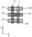
도 4는 본 발명의 일 실시예에 따른 반도체 디바이스의 예시적인 평면도를 도시하고 있다.
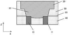
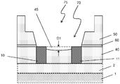
도 5-8은 본 발명의 일 실시예에 따른 다양한 제조 단계에서 반도체 디바이스의 예시적인 횡단면도를 도시하고 있다.
Claims (10)
- 반도체 디바이스를 제조하기 위한 방법에 있어서,
반도체 기판 위에서(over) 제1 방향으로 연장하는 복수의 하부 도전성 라인을 형성하는 단계;
상기 복수의 하부 도전성 라인 위에 놓이는 절연층을 형성하는 단계;
상기 절연층에 제1 개구를 형성하고, 상기 제1 개구를 도전성 재료로 충전함으로써, 복수의 제1 비아를 형성하는 단계;
상기 절연층에 제2 개구를 형성하고, 상기 제2 개구를 도전성 재료로 충전함으로써, 복수의 제2 비아를 형성하는 단계;
상기 제1 방향과 교차하는 제2 방향으로 연장하고, 상기 복수의 제1 비아에 접속되는 복수의 제1 상부 도전성 라인을 형성하는 단계; 및
상기 제2 방향으로 연장하고, 상기 복수의 제2 비아에 접속되는 복수의 제2 상부 도전성 라인을 형성하는 단계
를 포함하며,
상기 복수의 제1 비아를 형성하는 단계 및 상기 복수의 제2 비아를 형성하는 단계는, 별도의 패터닝 동작에 의해 수행되며,
상기 제1 개구를 형성하는 것과 상기 제2 개구를 형성하는 것 중 적어도 하나에서, 상기 복수의 하부 도전성 라인 중 2개의 라인의 적어도 일부가 적어도 하나의 개구에 노출되어, 적어도 하나의 비아가 상기 복수의 하부 도전성 라인 중 적어도 2개의 라인과 상기 복수의 제1 또는 제2 상부 도전성 라인 중 하나의 라인을 접속시키며,
상기 복수의 제1 상부 도전성 라인과 상기 복수의 제2 상부 도전성 라인은 제1 방향으로 제1 피치로 교호하여 배치되며,
상기 복수의 제1 비아는 상기 제1 방향으로 제2 피치로 배치되며, 상기 제2 피치는 상기 제1 피치의 2배인 것인 반도체 디바이스 제조 방법. - 청구항 1에 있어서,
상기 복수의 제2 비아는 상기 제1 방향으로 제2 피치로 배치되는 것인 반도체 디바이스 제조 방법. - 청구항 2에 있어서,
상기 복수의 제1 상부 도전성 라인은 상기 제1 방향으로 상기 제2 피치로 배치되며,
상기 복수의 제2 상부 도전성 라인은 상기 제1 방향으로 상기 제2 피치로 배치되는 것인 반도체 디바이스 제조 방법. - 청구항 1에 있어서,
상기 복수의 제1 비아 및 복수의 제1 상부 도전성 라인은 제1 이중 다마신 공정에 의해 형성되며,
상기 복수의 제2 비아 및 복수의 제2 상부 도전성 라인은 제2 이중 다마신 공정에 의해 형성되는 것인 반도체 디바이스 제조 방법. - 청구항 1에 있어서,
상기 복수의 제1 비아 및 상기 복수의 제2 비아는 동일한 설계 패턴을 가지며,
상기 복수의 제1 비아의 제1 방향으로의 평균 폭은, 상기 복수의 제2 비아의 제1 방향으로의 평균 폭과는 상이한 것인 반도체 디바이스 제조 방법. - 청구항 1에 있어서,
상기 제1 개구를 형성하는 것에서, 상기 복수의 하부 도전성 라인 중 2개의 라인의 적어도 일부가 상기 제1 개구 중 적어도 하나의 제1 개구에 노출되어, 상기 복수의 제1 비아 중 적어도 하나의 제1 비아가 상기 복수의 하부 도전성 라인 중 적어도 2개의 라인을 접속시키며,
상기 제2 개구를 형성하는 것에서, 상기 복수의 하부 도전성 라인 중 2개의 라인의 적어도 일부가 상기 제2 개구 중 적어도 하나의 제2 개구에 노출되어, 상기 복수의 제2 비아 중 적어도 하나의 제2 비아가 상기 복수의 하부 도전성 라인 중 적어도 2개의 라인을 접속시키는 것인 반도체 디바이스 제조 방법. - 청구항 6에 있어서,
상기 복수의 제1 비아 또는 상기 복수의 제2 비아 중 적어도 하나의 비아는, 하부 도전성 라인 중 단지 하나의 라인과 상기 복수의 제1 또는 제2 상부 도전성 라인 중 단지 하나의 라인을 접속시키는 것인 반도체 디바이스 제조 방법. - 청구항 6에 있어서,
상기 절연층을 형성하는 단계는, 제1 절연층, 상기 제1 절연층 위의 제2 절연층, 및 상기 제2 절연층 위의 제3 절연층을 형성하는 단계를 포함하며,
상기 제1 개구를 형성하는 것은,
상기 제2 절연층이 노출될 때까지, 상기 제3 절연층을 패터닝하는 단계; 및
상기 하부 도전성 라인 중 2개의 라인의 적어도 일부가 노출되도록, 상기 노출된 제2 절연층을 에칭하는 단계
를 포함하며,
상기 노출된 제2 절연층을 에칭하는 단계에서, 상기 제1 절연층의 상부 부분의 일부가 에칭되는 것인 반도체 디바이스 제조 방법. - 반도체 디바이스에 있어서,
반도체 기판 위에 놓이고, 제1 방향으로 연장하는 복수의 하부 도전성 라인;
상기 복수의 하부 도전성 라인 위에 놓이는 절연층;
상기 절연층 및 상기 제1 도전성 라인 위에 놓이고, 상기 제1 방향과 교차하는 제2 방향으로 연장하는 복수의 상부 도전성 라인; 및
상기 절연층에 형성되어 도전성 재료로 충전되는 복수의 비아
를 포함하며,
상기 복수의 상부 도전성 라인은 상기 제1 방향으로 제1 피치로 배치되고,
상기 복수의 비아는 제1 비아 및 제2 비아를 포함하며,
상기 제1 비아 중 적어도 하나의 비아는, 상기 복수의 하부 도전성 라인 중 적어도 2개의 라인과 상기 복수의 상부 도전성 라인 중 하나의 라인을 접속시키고,
상기 제1 비아의 상기 제1 방향으로의 평균 폭은, 상기 제2 비아의 상기 제1 방향으로의 평균 폭과는 상이한 것인 반도체 디바이스. - 반도체 디바이스에 있어서,
반도체 기판 위에 놓이고, 제1 방향으로 연장하며, 제1 하부 도전성 라인 및 상기 제1 방향과 교차하는 제2 방향으로 상기 제1 하부 도전성 라인에 인접한 제2 하부 도전성 라인을 포함하는 복수의 하부 도전성 라인;
상기 복수의 하부 도전성 라인 위에 놓이는 제1 절연층;
상기 절연층 및 상기 제1 도전성 라인 위에 놓이고, 상기 제2 방향으로 연장하며, 제1 상부 도전성 라인을 포함하는 복수의 상부 도전성 라인; 및
상기 절연층에 형성되어 도전성 재료로 충전되며, 제1 비아를 포함하는 복수의 비아
를 포함하며,
상기 제1 비아는 제1 및 제2 하부 도전성 라인과 상기 제1 상부 도전성 라인을 접속시키며,
상기 제1 비아에 충전된 도전성 재료의 최하부 부분은, 상기 제1 및 제2 하부 도전성 라인의 최상부 부분보다 상기 반도체 기판에 더 가까운 것인 반도체 디바이스.
Applications Claiming Priority (4)
| Application Number | Priority Date | Filing Date | Title |
|---|---|---|---|
| US201562272020P | 2015-12-28 | 2015-12-28 | |
| US62/272,020 | 2015-12-28 | ||
| US15/061,627 US10269697B2 (en) | 2015-12-28 | 2016-03-04 | Semiconductor device and manufacturing method thereof |
| US15/061,627 | 2016-03-04 |
Publications (2)
| Publication Number | Publication Date |
|---|---|
| KR20170077772A true KR20170077772A (ko) | 2017-07-06 |
| KR101925685B1 KR101925685B1 (ko) | 2018-12-05 |
Family
ID=59087953
Family Applications (1)
| Application Number | Title | Priority Date | Filing Date |
|---|---|---|---|
| KR1020160140199A Active KR101925685B1 (ko) | 2015-12-28 | 2016-10-26 | 반도체 디바이스 및 그 제조 방법 |
Country Status (5)
| Country | Link |
|---|---|
| US (3) | US10269697B2 (ko) |
| KR (1) | KR101925685B1 (ko) |
| CN (1) | CN107017198B (ko) |
| DE (1) | DE102016116090B4 (ko) |
| TW (1) | TWI651808B (ko) |
Families Citing this family (5)
| Publication number | Priority date | Publication date | Assignee | Title |
|---|---|---|---|---|
| US10269697B2 (en) * | 2015-12-28 | 2019-04-23 | Taiwan Semiconductor Manufacturing Co., Ltd. | Semiconductor device and manufacturing method thereof |
| CN109904111B (zh) * | 2017-12-11 | 2021-08-06 | 中芯国际集成电路制造(北京)有限公司 | 互连结构及其制造方法 |
| CN113242960B (zh) | 2018-12-20 | 2024-05-14 | 恩德斯+豪斯流量技术股份有限公司 | 科里奥利质量流量计 |
| US11756876B2 (en) * | 2020-04-01 | 2023-09-12 | Taiwan Semiconductor Manufacturing Company Ltd. | Semiconductor devices having power rails and signal tracks arranged in different layer |
| US12293913B1 (en) * | 2021-12-22 | 2025-05-06 | Intel Corporation | Directed self-assembly enabled subtractive metal patterning |
Family Cites Families (26)
| Publication number | Priority date | Publication date | Assignee | Title |
|---|---|---|---|---|
| JPH11330431A (ja) | 1998-05-18 | 1999-11-30 | Nec Corp | 不揮発性半導体記憶装置の製造方法 |
| JP3924550B2 (ja) | 2003-05-22 | 2007-06-06 | Necエレクトロニクス株式会社 | 半導体装置及びレイアウト装置及び方法並びにプログラム |
| US7538384B2 (en) | 2005-12-05 | 2009-05-26 | Taiwan Semiconductor Manufacturing Company, Ltd. | Non-volatile memory array structure |
| US8952547B2 (en) * | 2007-07-09 | 2015-02-10 | Taiwan Semiconductor Manufacturing Company, Ltd. | Semiconductor device with contact structure with first/second contacts formed in first/second dielectric layers and method of forming same |
| US8772933B2 (en) * | 2007-12-12 | 2014-07-08 | International Business Machines Corporation | Interconnect structure and method of making same |
| US20090321940A1 (en) * | 2008-06-30 | 2009-12-31 | Gerhard Kunkel | Method for Manufacturing Contact Openings, Method for Manufacturing an Integrated Circuit, an Integrated Circuit |
| DE102008049727A1 (de) | 2008-09-30 | 2010-07-01 | Advanced Micro Devices, Inc., Sunnyvale | Kontaktelemente und Kontaktdurchführungen eines Halbleiterbauelements, die durch eine Hartmaske und Doppelbelichtung hergestellt sind |
| KR20110002261A (ko) * | 2009-07-01 | 2011-01-07 | 삼성전자주식회사 | 더미를 포함하는 반도체 소자 |
| US8208305B2 (en) | 2009-12-23 | 2012-06-26 | Intel Corporation | Arrangement of pairs of NAND strings that share bitline contacts while utilizing distinct sources lines |
| US9041069B2 (en) | 2011-01-14 | 2015-05-26 | Taiwan Semiconductor Manufacturing Company, Ltd. | Distributed metal routing |
| US8513114B2 (en) | 2011-04-29 | 2013-08-20 | Renesas Electronics Corporation | Method for forming a dual damascene interconnect structure |
| US20130069170A1 (en) | 2011-09-19 | 2013-03-21 | Texas Instruments Incorporated | Illumination and design rule method for double patterned slotted contacts |
| US8779592B2 (en) * | 2012-05-01 | 2014-07-15 | Taiwan Semiconductor Manufacturing Company, Ltd. | Via-free interconnect structure with self-aligned metal line interconnections |
| US8813012B2 (en) * | 2012-07-16 | 2014-08-19 | Synopsys, Inc. | Self-aligned via interconnect using relaxed patterning exposure |
| US8835305B2 (en) * | 2012-07-31 | 2014-09-16 | International Business Machines Corporation | Method of fabricating a profile control in interconnect structures |
| US9461143B2 (en) | 2012-09-19 | 2016-10-04 | Intel Corporation | Gate contact structure over active gate and method to fabricate same |
| US9177914B2 (en) | 2012-11-15 | 2015-11-03 | Taiwan Semiconductor Manufacturing Company, Ltd. | Metal pad structure over TSV to reduce shorting of upper metal layer |
| US9230854B2 (en) * | 2013-04-08 | 2016-01-05 | Taiwan Semiconductor Manufacturing Company, Ltd. | Semiconductor device and method |
| US9236342B2 (en) | 2013-12-18 | 2016-01-12 | Intel Corporation | Self-aligned via and plug patterning with photobuckets for back end of line (BEOL) interconnects |
| US9613852B2 (en) * | 2014-03-21 | 2017-04-04 | Taiwan Semiconductor Manufacturing Company, Ltd. | Semiconductor structure and method making the same |
| US9721956B2 (en) | 2014-05-15 | 2017-08-01 | Taiwan Semiconductor Manufacturing Company Limited | Methods, structures and devices for intra-connection structures |
| WO2016025478A1 (en) * | 2014-08-11 | 2016-02-18 | Massachusetts Institute Of Technology | Interconnect structures for assembly of semiconductor structures including at least one integrated circuit structure |
| US9524935B2 (en) * | 2015-05-13 | 2016-12-20 | Globalfoundries Inc. | Filling cavities in an integrated circuit and resulting devices |
| JP2016225466A (ja) * | 2015-05-29 | 2016-12-28 | 株式会社東芝 | 半導体装置および半導体装置の製造方法 |
| US9576894B2 (en) * | 2015-06-03 | 2017-02-21 | GlobalFoundries, Inc. | Integrated circuits including organic interlayer dielectric layers and methods for fabricating the same |
| US10269697B2 (en) * | 2015-12-28 | 2019-04-23 | Taiwan Semiconductor Manufacturing Co., Ltd. | Semiconductor device and manufacturing method thereof |
-
2016
- 2016-03-04 US US15/061,627 patent/US10269697B2/en active Active
- 2016-08-30 DE DE102016116090.3A patent/DE102016116090B4/de active Active
- 2016-09-07 TW TW105128879A patent/TWI651808B/zh active
- 2016-10-26 KR KR1020160140199A patent/KR101925685B1/ko active Active
- 2016-11-29 CN CN201611073787.XA patent/CN107017198B/zh active Active
-
2018
- 2018-11-20 US US16/196,366 patent/US10629527B2/en active Active
-
2020
- 2020-03-06 US US16/811,873 patent/US11177211B2/en active Active
Also Published As
| Publication number | Publication date |
|---|---|
| US20200211957A1 (en) | 2020-07-02 |
| TWI651808B (zh) | 2019-02-21 |
| CN107017198B (zh) | 2020-01-14 |
| US10269697B2 (en) | 2019-04-23 |
| US20170186686A1 (en) | 2017-06-29 |
| US11177211B2 (en) | 2021-11-16 |
| US10629527B2 (en) | 2020-04-21 |
| KR101925685B1 (ko) | 2018-12-05 |
| DE102016116090A1 (de) | 2017-06-29 |
| TW201735248A (zh) | 2017-10-01 |
| CN107017198A (zh) | 2017-08-04 |
| US20190109087A1 (en) | 2019-04-11 |
| DE102016116090B4 (de) | 2021-08-12 |
Similar Documents
| Publication | Publication Date | Title |
|---|---|---|
| US11676895B2 (en) | Semiconductor device comprising air gaps having different configurations | |
| US12424448B2 (en) | Reduction of line wiggling | |
| TWI605561B (zh) | 具有蝕刻停止層於傳導線上方的互連結構 | |
| CN102820280B (zh) | 用于集成电路的非分层式金属层 | |
| KR100902581B1 (ko) | 반도체 소자의 스택 커패시터 및 그의 형성방법 | |
| US11177211B2 (en) | Method of manufacturing via structures of semiconductor devices | |
| US9613903B2 (en) | Fine line space resolution lithography structure for integrated circuit features using double patterning technology | |
| US20130285246A1 (en) | Semiconductor Device With Self-Aligned Interconnects and Blocking Portions | |
| TWI588901B (zh) | 自對準通孔流程 | |
| US9627310B2 (en) | Semiconductor device with self-aligned interconnects | |
| KR102774731B1 (ko) | 반도체 디바이스 및 그 제조 방법 | |
| CN109524348B (zh) | 基本规则区域中的完全对准的过孔 | |
| KR20080061030A (ko) | 반도체 소자의 금속 배선 형성 방법 | |
| TW201732930A (zh) | 半導體裝置之形成方法 | |
| TW201830579A (zh) | 半導體裝置結構 | |
| KR102751635B1 (ko) | 반도체 디바이스 및 그 제조 방법 | |
| KR100408683B1 (ko) | 반도체 소자의 콘택 형성방법 | |
| US12293970B2 (en) | Semiconductor structure and method for manufacturing thereof | |
| CN120933262A (zh) | 包括互连结构的半导体器件及其制造方法 | |
| KR100582410B1 (ko) | 반도체 장치 및 반도체 장치의 제조방법 | |
| KR20070031621A (ko) | 반도체 소자 제조 방법 | |
| KR20070069883A (ko) | 반도체 소자 및 그 제조방법 |
Legal Events
| Date | Code | Title | Description |
|---|---|---|---|
| A201 | Request for examination | ||
| PA0109 | Patent application |
St.27 status event code: A-0-1-A10-A12-nap-PA0109 |
|
| PA0201 | Request for examination |
St.27 status event code: A-1-2-D10-D11-exm-PA0201 |
|
| PG1501 | Laying open of application |
St.27 status event code: A-1-1-Q10-Q12-nap-PG1501 |
|
| D13-X000 | Search requested |
St.27 status event code: A-1-2-D10-D13-srh-X000 |
|
| D14-X000 | Search report completed |
St.27 status event code: A-1-2-D10-D14-srh-X000 |
|
| E902 | Notification of reason for refusal | ||
| PE0902 | Notice of grounds for rejection |
St.27 status event code: A-1-2-D10-D21-exm-PE0902 |
|
| T11-X000 | Administrative time limit extension requested |
St.27 status event code: U-3-3-T10-T11-oth-X000 |
|
| T11-X000 | Administrative time limit extension requested |
St.27 status event code: U-3-3-T10-T11-oth-X000 |
|
| P11-X000 | Amendment of application requested |
St.27 status event code: A-2-2-P10-P11-nap-X000 |
|
| P13-X000 | Application amended |
St.27 status event code: A-2-2-P10-P13-nap-X000 |
|
| E701 | Decision to grant or registration of patent right | ||
| PE0701 | Decision of registration |
St.27 status event code: A-1-2-D10-D22-exm-PE0701 |
|
| GRNT | Written decision to grant | ||
| PR0701 | Registration of establishment |
St.27 status event code: A-2-4-F10-F11-exm-PR0701 |
|
| PR1002 | Payment of registration fee |
St.27 status event code: A-2-2-U10-U11-oth-PR1002 Fee payment year number: 1 |
|
| PG1601 | Publication of registration |
St.27 status event code: A-4-4-Q10-Q13-nap-PG1601 |
|
| R18-X000 | Changes to party contact information recorded |
St.27 status event code: A-5-5-R10-R18-oth-X000 |
|
| PR1001 | Payment of annual fee |
St.27 status event code: A-4-4-U10-U11-oth-PR1001 Fee payment year number: 4 |
|
| PR1001 | Payment of annual fee |
St.27 status event code: A-4-4-U10-U11-oth-PR1001 Fee payment year number: 5 |
|
| PR1001 | Payment of annual fee |
St.27 status event code: A-4-4-U10-U11-oth-PR1001 Fee payment year number: 6 |
|
| PR1001 | Payment of annual fee |
St.27 status event code: A-4-4-U10-U11-oth-PR1001 Fee payment year number: 7 |
|
| PR1001 | Payment of annual fee |
St.27 status event code: A-4-4-U10-U11-oth-PR1001 Fee payment year number: 8 |
|
| U11 | Full renewal or maintenance fee paid |
Free format text: ST27 STATUS EVENT CODE: A-4-4-U10-U11-OTH-PR1001 (AS PROVIDED BY THE NATIONAL OFFICE) Year of fee payment: 8 |
|
| P22-X000 | Classification modified |
St.27 status event code: A-4-4-P10-P22-nap-X000 |