KR20170094301A - 반도체 웨이퍼의 처리 방법, 반도체 칩 및 표면 보호 테이프 - Google Patents
반도체 웨이퍼의 처리 방법, 반도체 칩 및 표면 보호 테이프 Download PDFInfo
- Publication number
- KR20170094301A KR20170094301A KR1020177018635A KR20177018635A KR20170094301A KR 20170094301 A KR20170094301 A KR 20170094301A KR 1020177018635 A KR1020177018635 A KR 1020177018635A KR 20177018635 A KR20177018635 A KR 20177018635A KR 20170094301 A KR20170094301 A KR 20170094301A
- Authority
- KR
- South Korea
- Prior art keywords
- semiconductor wafer
- sensitive adhesive
- pressure
- adhesive layer
- tape
- Prior art date
- Legal status (The legal status is an assumption and is not a legal conclusion. Google has not performed a legal analysis and makes no representation as to the accuracy of the status listed.)
- Granted
Links
Images


Classifications
-
- H01L21/78—
-
- H—ELECTRICITY
- H10—SEMICONDUCTOR DEVICES; ELECTRIC SOLID-STATE DEVICES NOT OTHERWISE PROVIDED FOR
- H10P—GENERIC PROCESSES OR APPARATUS FOR THE MANUFACTURE OR TREATMENT OF DEVICES COVERED BY CLASS H10
- H10P72/00—Handling or holding of wafers, substrates or devices during manufacture or treatment thereof
- H10P72/70—Handling or holding of wafers, substrates or devices during manufacture or treatment thereof for supporting or gripping
- H10P72/74—Handling or holding of wafers, substrates or devices during manufacture or treatment thereof for supporting or gripping using temporarily an auxiliary support
- H10P72/7402—Wafer tapes, e.g. grinding or dicing support tapes
-
- H01L21/3065—
-
- H01L21/67712—
-
- H01L21/67721—
-
- H01L21/6836—
-
- H—ELECTRICITY
- H10—SEMICONDUCTOR DEVICES; ELECTRIC SOLID-STATE DEVICES NOT OTHERWISE PROVIDED FOR
- H10P—GENERIC PROCESSES OR APPARATUS FOR THE MANUFACTURE OR TREATMENT OF DEVICES COVERED BY CLASS H10
- H10P50/00—Etching of wafers, substrates or parts of devices
-
- H—ELECTRICITY
- H10—SEMICONDUCTOR DEVICES; ELECTRIC SOLID-STATE DEVICES NOT OTHERWISE PROVIDED FOR
- H10P—GENERIC PROCESSES OR APPARATUS FOR THE MANUFACTURE OR TREATMENT OF DEVICES COVERED BY CLASS H10
- H10P50/00—Etching of wafers, substrates or parts of devices
- H10P50/20—Dry etching; Plasma etching; Reactive-ion etching
- H10P50/24—Dry etching; Plasma etching; Reactive-ion etching of semiconductor materials
- H10P50/242—Dry etching; Plasma etching; Reactive-ion etching of semiconductor materials of Group IV materials
-
- H—ELECTRICITY
- H10—SEMICONDUCTOR DEVICES; ELECTRIC SOLID-STATE DEVICES NOT OTHERWISE PROVIDED FOR
- H10P—GENERIC PROCESSES OR APPARATUS FOR THE MANUFACTURE OR TREATMENT OF DEVICES COVERED BY CLASS H10
- H10P54/00—Cutting or separating of wafers, substrates or parts of devices
-
- H—ELECTRICITY
- H10—SEMICONDUCTOR DEVICES; ELECTRIC SOLID-STATE DEVICES NOT OTHERWISE PROVIDED FOR
- H10P—GENERIC PROCESSES OR APPARATUS FOR THE MANUFACTURE OR TREATMENT OF DEVICES COVERED BY CLASS H10
- H10P72/00—Handling or holding of wafers, substrates or devices during manufacture or treatment thereof
- H10P72/30—Handling or holding of wafers, substrates or devices during manufacture or treatment thereof for conveying, e.g. between different workstations
- H10P72/32—Handling or holding of wafers, substrates or devices during manufacture or treatment thereof for conveying, e.g. between different workstations between different workstations
- H10P72/3206—Handling or holding of wafers, substrates or devices during manufacture or treatment thereof for conveying, e.g. between different workstations between different workstations the substrate being handled substantially vertically
-
- H—ELECTRICITY
- H10—SEMICONDUCTOR DEVICES; ELECTRIC SOLID-STATE DEVICES NOT OTHERWISE PROVIDED FOR
- H10P—GENERIC PROCESSES OR APPARATUS FOR THE MANUFACTURE OR TREATMENT OF DEVICES COVERED BY CLASS H10
- H10P72/00—Handling or holding of wafers, substrates or devices during manufacture or treatment thereof
- H10P72/30—Handling or holding of wafers, substrates or devices during manufacture or treatment thereof for conveying, e.g. between different workstations
- H10P72/32—Handling or holding of wafers, substrates or devices during manufacture or treatment thereof for conveying, e.g. between different workstations between different workstations
- H10P72/3212—Handling or holding of wafers, substrates or devices during manufacture or treatment thereof for conveying, e.g. between different workstations between different workstations the substrates to be conveyed not being semiconductor wafers or large planar substrates, e.g. chips or lead frames
-
- H—ELECTRICITY
- H10—SEMICONDUCTOR DEVICES; ELECTRIC SOLID-STATE DEVICES NOT OTHERWISE PROVIDED FOR
- H10W—GENERIC PACKAGES, INTERCONNECTIONS, CONNECTORS OR OTHER CONSTRUCTIONAL DETAILS OF DEVICES COVERED BY CLASS H10
- H10W72/00—Interconnections or connectors in packages
- H10W72/01—Manufacture or treatment
- H10W72/013—Manufacture or treatment of die-attach connectors
Landscapes
- Dicing (AREA)
- Engineering & Computer Science (AREA)
- Physics & Mathematics (AREA)
- Plasma & Fusion (AREA)
- Manufacturing & Machinery (AREA)
Abstract
Description
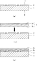
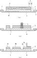
도 2는, 본 발명의 제1 실시형태에 있어서의 반도체 웨이퍼의 박막화와 고정까지의 공정을 설명하는 개략 단면도이며, 도 2(a)는 반도체 웨이퍼의 박막화 처리를 나타내고, 도 2(b)는 웨이퍼 고정 테이프를 맞붙이는 모습을 나타내고, 도 2(c)는 반도체 웨이퍼를 링 프레임에 고정한 상태를 나타낸다.
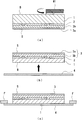
도 3은, 본 발명의 제1 실시형태에 있어서의 마스크 형성까지의 공정을 설명하는 개략 단면도이며, 도 3(a)는 표면 보호 테이프로부터 기재 필름을 당겨서 박리하는 모습을 나타내고, 도 3(b)는 표면 보호 테이프의 점착제층이 노출된 상태를 나타내고, 도 3(c)는 레이저로 스트리트에 상당하는 점착제층을 잘라내는 공정을 나타낸다.
도 4는, 본 발명의 제1 실시형태에 있어서의 플라즈마 다이싱과 플라즈마 에싱의 공정을 설명하는 개략 단면도이며, 도 4(a)는 플라즈마 다이싱을 행하는 모습을 나타내고, 도 4(b)는 칩으로 개편화된 상태를 나타내고, 도 4(c)는 플라즈마 에싱을 행하는 모습을 나타낸다.
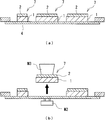
도 5는, 본 발명의 제1 실시형태에 있어서의 칩을 픽업할 때까지의 공정을 설명하는 개략 단면도이며, 도 5(a)는 마스크가 된 점착제층이 제거된 상태를 나타내고, 도 5(b)는 칩을 픽업하는 모습을 나타낸다.
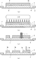
도 6은, 본 발명의 제2 실시형태에 있어서의 자외선 조사 처리를 행하는 전후 상태를 설명하는 개략 단면도이며, 도 6(a)는 반도체 웨이퍼의 표리 양면을 각각 표면 보호 테이프와 웨이퍼 고정 테이프로 피복하고 고정한 상태를 나타내고, 도 6(b)는 자외선이 조사되는 모습을 나타내고, 도 6(c)는 표면 보호 테이프로부터 기재 필름을 당겨서 박리하는 모습을 나타낸다.
도 7은, 본 발명의 제3 실시형태에 있어서의 레이저로 마스크 형성을 행하는 전후 상태를 설명하는 개략 단면도이며, 도 7(a)는 반도체 웨이퍼의 표리 양면을 각각 표면 보호 테이프와 웨이퍼 고정 테이프로 피복하고 고정한 상태를 나타내고, 도 7(b)는 레이저로 스트리트 부분에 상당하는 점착제층을 잘라내는 공정을 나타내고, 도 7(c)는 표면 보호 테이프로부터 기재 필름을 당겨서 박리하는 모습을 나타낸다.
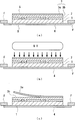
도 8은, 본 발명의 제4 실시형태에 있어서의 기재 필름을 당겨서 박리할 때까지의 공정을 설명하는 개략 단면도이며, 도 8(a)는 반도체 웨이퍼의 표리 양면을 각각 표면 보호 테이프와 웨이퍼 고정 테이프로 피복하고 고정한 상태를 나타내고, 도 8(b)는 자외선이 조사되는 모습을 나타내고, 도 8(c)는 레이저로 스트리트 부분에 상당하는 표면 보호 테이프를 잘라내는 공정을 나타내고, 도 8(d)은 기재 필름을 당겨서 박리하는 모습을 나타낸다.

2: 패턴면
3: 표면 보호 테이프
3a: 기재 필름
3b: 점착제층
4: 웨이퍼 고정 테이프
4a: 점착제층 또는 접착제층
4b: 기재 필름
7: 칩
S: 표면
B: 이면
M1: 웨이퍼 연삭 장치
M2: 핀
M3: 콜릿
F: 링 프레임
L: CO2 레이저
P1: SF6 가스의 플라즈마
P2: O2 가스의 플라즈마
Claims (9)
- 반도체 웨이퍼의 처리 방법으로서,
(a) 패턴면측에, 기재 필름 상에 점착제층을 가지는 표면 보호 테이프가 맞붙인 상태에서 반도체 웨이퍼의 이면을 연삭하고, 연삭한 이면에 웨이퍼 고정 테이프를 맞붙여서, 링 프레임으로 지지 고정하는 공정,
(b) 상기 반도체 웨이퍼의 스트리트에 상당하는 부분의 CO2 레이저에 의한 절단 및 상기 기재 필름의 박리를 포함하는 공정에 의해, 반도체 웨이퍼의 패턴면측으로부터 스트리트를 개구하는 공정,
(c) SF6 플라즈마에 의해 반도체 웨이퍼를 상기 스트리트에서 분단하여 반도체 칩으로 개편화하는 플라즈마 다이싱 공정, 및,
(d) O2 플라즈마에 의해 상기 점착제층을 제거하는 에싱 공정을 포함하는 것을 특징으로 하는 반도체 웨이퍼의 처리 방법. - 제 1 항에 있어서,
상기 (b) 공정이, (i) 반도체 웨이퍼의 패턴면에 맞붙인 상기 표면 보호 테이프로부터 상기 기재 필름을 박리하여 상기 점착제층을 표출시키는 공정, 및, (ii) 상기 표출된 점착제층 중 반도체 웨이퍼의 스트리트에 상당하는 부분을 CO2 레이저로 절단하여 반도체 웨이퍼의 스트리트를 개구하는 공정인 것을 특징으로 하는 반도체 웨이퍼의 처리 방법. - 제 1 항에 있어서,
상기 (b) 공정이, (iii) 반도체 웨이퍼의 패턴면에 맞붙인 상기 표면 보호 테이프 중 반도체 웨이퍼의 스트리트에 상당하는 부분을 CO2 레이저로 절단하여 반도체 웨이퍼의 스트리트를 개구하는 공정, 및, (iv) 상기 표면 보호 테이프로부터 상기 기재 필름을 박리하여 상기 점착제층을 표출시키는 공정인 것을 특징으로 하는 반도체 웨이퍼의 처리 방법. - 제 1 항 내지 제 3 항 중 어느 한 항에 있어서,
상기 기재 필름을 박리하기 이전에 자외선을 조사하여 상기 점착제층을 경화시키는 공정을 포함하는 것을 특징으로 하는 반도체 웨이퍼의 처리 방법. - 제 1 항 내지 제 4 항 중 어느 한 항에 있어서,
상기 (a) 공정의 웨이퍼 고정 테이프가, 다이싱 테이프 또는 다이싱 다이본딩 테이프인 것을 특징으로 하는 반도체 웨이퍼의 처리 방법. - 제 1 항 내지 제 5 항 중 어느 한 항에 있어서,
상기 (d) 공정 후, 웨이퍼 고정 테이프로부터 칩을 픽업하는 공정을 포함하는 것을 특징으로 하는 반도체 웨이퍼의 처리 방법. - 제 6 항에 있어서,
픽업한 칩을 다이본딩 공정으로 이행하는 공정을 포함하는 것을 특징으로 하는 반도체 웨이퍼의 처리 방법. - 제 1 항 내지 제 7 항 중 어느 한 항에 기재된 반도체 웨이퍼의 처리 방법에 의해서 제조되어 이루어지는 것을 특징으로 하는 반도체 칩.
- 제 1 항 내지 제 7 항 중 어느 한 항에 기재된 반도체 웨이퍼의 처리 방법에서 이용하는 것을 특징으로 하는 표면 보호 테이프.
Applications Claiming Priority (3)
| Application Number | Priority Date | Filing Date | Title |
|---|---|---|---|
| JP2015051482A JP6738591B2 (ja) | 2015-03-13 | 2015-03-13 | 半導体ウェハの処理方法、半導体チップおよび表面保護テープ |
| JPJP-P-2015-051482 | 2015-03-13 | ||
| PCT/JP2016/057615 WO2016148025A1 (ja) | 2015-03-13 | 2016-03-10 | 半導体ウェハの処理方法、半導体チップおよび表面保護テープ |
Publications (2)
| Publication Number | Publication Date |
|---|---|
| KR20170094301A true KR20170094301A (ko) | 2017-08-17 |
| KR102070031B1 KR102070031B1 (ko) | 2020-01-29 |
Family
ID=56918690
Family Applications (1)
| Application Number | Title | Priority Date | Filing Date |
|---|---|---|---|
| KR1020177018635A Active KR102070031B1 (ko) | 2015-03-13 | 2016-03-10 | 반도체 웨이퍼의 처리 방법, 반도체 칩 및 표면 보호 테이프 |
Country Status (5)
| Country | Link |
|---|---|
| US (1) | US10418267B2 (ko) |
| JP (1) | JP6738591B2 (ko) |
| KR (1) | KR102070031B1 (ko) |
| CN (1) | CN107210204B (ko) |
| WO (1) | WO2016148025A1 (ko) |
Cited By (1)
| Publication number | Priority date | Publication date | Assignee | Title |
|---|---|---|---|---|
| KR20190098247A (ko) * | 2017-03-31 | 2019-08-21 | 후루카와 덴키 고교 가부시키가이샤 | 박리 라이너 부착 마스크 일체형 표면 보호 테이프 |
Families Citing this family (37)
| Publication number | Priority date | Publication date | Assignee | Title |
|---|---|---|---|---|
| US11069734B2 (en) | 2014-12-11 | 2021-07-20 | Invensas Corporation | Image sensor device |
| US9741620B2 (en) * | 2015-06-24 | 2017-08-22 | Invensas Corporation | Structures and methods for reliable packages |
| CN107210207A (zh) * | 2015-11-09 | 2017-09-26 | 古河电气工业株式会社 | 半导体芯片的制造方法和用于该制造方法的掩模一体型表面保护带 |
| US10204893B2 (en) | 2016-05-19 | 2019-02-12 | Invensas Bonding Technologies, Inc. | Stacked dies and methods for forming bonded structures |
| JP6524558B2 (ja) * | 2016-12-15 | 2019-06-05 | パナソニックIpマネジメント株式会社 | 素子チップの製造方法 |
| US10269756B2 (en) | 2017-04-21 | 2019-04-23 | Invensas Bonding Technologies, Inc. | Die processing |
| US10879212B2 (en) | 2017-05-11 | 2020-12-29 | Invensas Bonding Technologies, Inc. | Processed stacked dies |
| US10217720B2 (en) | 2017-06-15 | 2019-02-26 | Invensas Corporation | Multi-chip modules formed using wafer-level processing of a reconstitute wafer |
| JP7042437B2 (ja) | 2017-09-07 | 2022-03-28 | パナソニックIpマネジメント株式会社 | 素子チップの製造方法 |
| JP6990577B2 (ja) * | 2017-12-22 | 2022-01-12 | 東レエンジニアリング株式会社 | 実装方法および実装装置 |
| US10727219B2 (en) | 2018-02-15 | 2020-07-28 | Invensas Bonding Technologies, Inc. | Techniques for processing devices |
| JP7042667B2 (ja) * | 2018-03-28 | 2022-03-28 | 古河電気工業株式会社 | 半導体チップの製造方法 |
| US11276676B2 (en) | 2018-05-15 | 2022-03-15 | Invensas Bonding Technologies, Inc. | Stacked devices and methods of fabrication |
| WO2020010136A1 (en) | 2018-07-06 | 2020-01-09 | Invensas Bonding Technologies, Inc. | Molded direct bonded and interconnected stack |
| US11462419B2 (en) | 2018-07-06 | 2022-10-04 | Invensas Bonding Technologies, Inc. | Microelectronic assemblies |
| CN111112808A (zh) * | 2018-10-30 | 2020-05-08 | 三星钻石工业股份有限公司 | 基板分断装置及基板分断方法 |
| CN113039628A (zh) * | 2018-11-15 | 2021-06-25 | 东京应化工业株式会社 | 等离子体切割用保护膜形成剂及半导体芯片的制造方法 |
| KR102677473B1 (ko) | 2018-11-22 | 2024-06-24 | 삼성디스플레이 주식회사 | 원장보호필름의 박리방법, 유기발광 표시장치의 제조방법, 및 유기발광 표시장치 |
| KR102552270B1 (ko) | 2018-11-22 | 2023-07-07 | 삼성디스플레이 주식회사 | 원장보호필름의 박리방법 및 유기발광 표시장치의 제조방법 |
| CN113330557A (zh) | 2019-01-14 | 2021-08-31 | 伊文萨思粘合技术公司 | 键合结构 |
| CN111916359B (zh) * | 2019-05-09 | 2022-04-26 | 矽磐微电子(重庆)有限公司 | 半导体封装方法及半导体封装结构 |
| US11296053B2 (en) | 2019-06-26 | 2022-04-05 | Invensas Bonding Technologies, Inc. | Direct bonded stack structures for increased reliability and improved yield in microelectronics |
| US12080672B2 (en) | 2019-09-26 | 2024-09-03 | Adeia Semiconductor Bonding Technologies Inc. | Direct gang bonding methods including directly bonding first element to second element to form bonded structure without adhesive |
| KR20220119634A (ko) | 2019-12-24 | 2022-08-30 | 도오꾜오까고오교 가부시끼가이샤 | 보호막 형성제, 및 반도체 칩의 제조 방법 |
| CN111050258A (zh) * | 2019-12-31 | 2020-04-21 | 歌尔股份有限公司 | 防尘结构、麦克风封装结构以及电子设备 |
| US11742314B2 (en) | 2020-03-31 | 2023-08-29 | Adeia Semiconductor Bonding Technologies Inc. | Reliable hybrid bonded apparatus |
| US11631647B2 (en) | 2020-06-30 | 2023-04-18 | Adeia Semiconductor Bonding Technologies Inc. | Integrated device packages with integrated device die and dummy element |
| US11764177B2 (en) | 2020-09-04 | 2023-09-19 | Adeia Semiconductor Bonding Technologies Inc. | Bonded structure with interconnect structure |
| US11728273B2 (en) | 2020-09-04 | 2023-08-15 | Adeia Semiconductor Bonding Technologies Inc. | Bonded structure with interconnect structure |
| WO2022067644A1 (en) | 2020-09-30 | 2022-04-07 | Innoscience (Suzhou) Technology Co., Ltd. | Semiconductor device and method for manufacturing the same |
| GB202020022D0 (en) * | 2020-12-17 | 2021-02-03 | Spts Technologies Ltd | Method and apparatus |
| US12550799B2 (en) | 2021-03-31 | 2026-02-10 | Adeia Semiconductor Bonding Technologies Inc. | Direct bonding methods and structures |
| US12604771B2 (en) | 2021-10-28 | 2026-04-14 | Adeia Semiconductor Bonding Technologies Inc. | Direct bonding methods and structures |
| US12667031B2 (en) | 2021-12-23 | 2026-06-23 | Adeia Semiconductor Bonding Technologies Inc. | Direct bonding on package substrates |
| CN116705700A (zh) * | 2022-02-24 | 2023-09-05 | 星科金朋私人有限公司 | 制造半导体封装的方法 |
| KR102617333B1 (ko) | 2023-02-10 | 2023-12-21 | 변영기 | 웨이퍼 테이프 분리 방지시스템 |
| TR2024006173A1 (tr) * | 2024-05-20 | 2025-11-21 | Bilkent Ueniversitesi Ulusal Nanoteknoloji Arastirma Merkezi | Yongalardan ayirma bandinin yonga yüzeyi̇nden tamamen temi̇zlenmesi̇ni̇ sağlayan bi̇r yöntem |
Citations (9)
| Publication number | Priority date | Publication date | Assignee | Title |
|---|---|---|---|---|
| JP2002151440A (ja) * | 2000-11-14 | 2002-05-24 | Sekisui Chem Co Ltd | ウェーハダイシング方法及びその装置 |
| JP2003179005A (ja) * | 2001-12-13 | 2003-06-27 | Tokyo Electron Ltd | 半導体素子分離方法及び半導体素子分離装置 |
| US20030176069A1 (en) * | 2002-03-14 | 2003-09-18 | Tokyo Electron Limited | Plasma processing apparatus and plasma processing method |
| JP2007019385A (ja) | 2005-07-11 | 2007-01-25 | Matsushita Electric Ind Co Ltd | 半導体チップの製造方法 |
| JP2007019386A (ja) * | 2005-07-11 | 2007-01-25 | Matsushita Electric Ind Co Ltd | 半導体チップの製造方法 |
| JP2009033087A (ja) * | 2006-12-05 | 2009-02-12 | Furukawa Electric Co Ltd:The | 半導体ウェハの処理方法 |
| KR20090115039A (ko) * | 2007-02-08 | 2009-11-04 | 파나소닉 주식회사 | 반도체칩의 제조 방법 |
| JP2010165963A (ja) * | 2009-01-19 | 2010-07-29 | Furukawa Electric Co Ltd:The | 半導体ウェハの処理方法 |
| JP2014523110A (ja) * | 2011-06-15 | 2014-09-08 | アプライド マテリアルズ インコーポレイテッド | レーザスクライビング・プラズマエッチングによるデバイスの個片化用のインサイチュー蒸着マスク層 |
Family Cites Families (28)
| Publication number | Priority date | Publication date | Assignee | Title |
|---|---|---|---|---|
| JPH05198542A (ja) * | 1991-09-02 | 1993-08-06 | Mitsui Toatsu Chem Inc | 半導体ウエハの裏面研削方法および該方法に用いる粘着テープ |
| JP3481307B2 (ja) * | 1994-07-05 | 2003-12-22 | 古河電気工業株式会社 | 半導体ウエハ表面保護用粘着テープ |
| JPH1027971A (ja) * | 1996-07-10 | 1998-01-27 | Nec Corp | 有機薄膜多層配線基板の切断方法 |
| JP2002100588A (ja) * | 2000-09-22 | 2002-04-05 | Shinkawa Ltd | 半導体装置の製造方法 |
| US6703244B2 (en) * | 2001-07-20 | 2004-03-09 | William A. Croft | Method for confirming presence of mycotoxicosis |
| JP4013745B2 (ja) * | 2002-11-20 | 2007-11-28 | 松下電器産業株式会社 | プラズマ処理方法 |
| US6897128B2 (en) * | 2002-11-20 | 2005-05-24 | Matsushita Electric Industrial Co., Ltd. | Method of manufacturing semiconductor device, plasma processing apparatus and plasma processing method |
| JP4018088B2 (ja) * | 2004-08-02 | 2007-12-05 | 松下電器産業株式会社 | 半導体ウェハの分割方法及び半導体素子の製造方法 |
| JP2006344795A (ja) * | 2005-06-09 | 2006-12-21 | Disco Abrasive Syst Ltd | ウエーハの分割方法 |
| JP4840200B2 (ja) * | 2007-03-09 | 2011-12-21 | パナソニック株式会社 | 半導体チップの製造方法 |
| JP2009043992A (ja) * | 2007-08-09 | 2009-02-26 | Disco Abrasive Syst Ltd | ウエーハの加工方法 |
| JP2009260272A (ja) * | 2008-03-25 | 2009-11-05 | Panasonic Corp | 基板の加工方法および半導体チップの製造方法ならびに樹脂接着層付き半導体チップの製造方法 |
| US7655539B2 (en) * | 2008-04-16 | 2010-02-02 | Fairchild Semiconductor Corporation | Dice by grind for back surface metallized dies |
| TWI601242B (zh) * | 2010-01-18 | 2017-10-01 | 半導體組件工業公司 | 半導體晶片分割方法 |
| US8642448B2 (en) * | 2010-06-22 | 2014-02-04 | Applied Materials, Inc. | Wafer dicing using femtosecond-based laser and plasma etch |
| US9343365B2 (en) * | 2011-03-14 | 2016-05-17 | Plasma-Therm Llc | Method and apparatus for plasma dicing a semi-conductor wafer |
| JP5591181B2 (ja) * | 2011-05-19 | 2014-09-17 | パナソニック株式会社 | 半導体チップの製造方法 |
| JP5294358B2 (ja) * | 2012-01-06 | 2013-09-18 | 古河電気工業株式会社 | ウエハ加工用テープ及びこれを使用した半導体装置の製造方法 |
| JP5901422B2 (ja) * | 2012-05-15 | 2016-04-13 | 古河電気工業株式会社 | 半導体ウェハのダイシング方法およびこれに用いる半導体加工用ダイシングテープ |
| JP6078272B2 (ja) * | 2012-09-10 | 2017-02-08 | 株式会社ディスコ | ウエーハの加工方法 |
| US9460966B2 (en) * | 2013-10-10 | 2016-10-04 | Applied Materials, Inc. | Method and apparatus for dicing wafers having thick passivation polymer layer |
| US20150147850A1 (en) * | 2013-11-25 | 2015-05-28 | Infineon Technologies Ag | Methods for processing a semiconductor workpiece |
| US9349648B2 (en) * | 2014-07-22 | 2016-05-24 | Applied Materials, Inc. | Hybrid wafer dicing approach using a rectangular shaped two-dimensional top hat laser beam profile or a linear shaped one-dimensional top hat laser beam profile laser scribing process and plasma etch process |
| JP2016039186A (ja) * | 2014-08-05 | 2016-03-22 | 株式会社ディスコ | ウエーハの加工方法 |
| US9355907B1 (en) * | 2015-01-05 | 2016-05-31 | Applied Materials, Inc. | Hybrid wafer dicing approach using a line shaped laser beam profile laser scribing process and plasma etch process |
| CN106024566B (zh) * | 2015-03-31 | 2019-07-05 | 松下知识产权经营株式会社 | 等离子处理装置以及等离子处理方法 |
| US9852997B2 (en) * | 2016-03-25 | 2017-12-26 | Applied Materials, Inc. | Hybrid wafer dicing approach using a rotating beam laser scribing process and plasma etch process |
| JP6524553B2 (ja) * | 2016-05-30 | 2019-06-05 | パナソニックIpマネジメント株式会社 | 素子チップの製造方法 |
-
2015
- 2015-03-13 JP JP2015051482A patent/JP6738591B2/ja active Active
-
2016
- 2016-03-10 WO PCT/JP2016/057615 patent/WO2016148025A1/ja not_active Ceased
- 2016-03-10 CN CN201680005367.XA patent/CN107210204B/zh not_active Expired - Fee Related
- 2016-03-10 KR KR1020177018635A patent/KR102070031B1/ko active Active
-
2017
- 2017-09-12 US US15/702,021 patent/US10418267B2/en not_active Expired - Fee Related
Patent Citations (10)
| Publication number | Priority date | Publication date | Assignee | Title |
|---|---|---|---|---|
| JP2002151440A (ja) * | 2000-11-14 | 2002-05-24 | Sekisui Chem Co Ltd | ウェーハダイシング方法及びその装置 |
| JP2003179005A (ja) * | 2001-12-13 | 2003-06-27 | Tokyo Electron Ltd | 半導体素子分離方法及び半導体素子分離装置 |
| US20030176069A1 (en) * | 2002-03-14 | 2003-09-18 | Tokyo Electron Limited | Plasma processing apparatus and plasma processing method |
| JP2007019385A (ja) | 2005-07-11 | 2007-01-25 | Matsushita Electric Ind Co Ltd | 半導体チップの製造方法 |
| JP2007019386A (ja) * | 2005-07-11 | 2007-01-25 | Matsushita Electric Ind Co Ltd | 半導体チップの製造方法 |
| JP2009033087A (ja) * | 2006-12-05 | 2009-02-12 | Furukawa Electric Co Ltd:The | 半導体ウェハの処理方法 |
| KR20090115039A (ko) * | 2007-02-08 | 2009-11-04 | 파나소닉 주식회사 | 반도체칩의 제조 방법 |
| US20100173474A1 (en) * | 2007-02-08 | 2010-07-08 | Matsushita Electric Industrial Co., Ltd. | Method of manufacturing semiconductor chip |
| JP2010165963A (ja) * | 2009-01-19 | 2010-07-29 | Furukawa Electric Co Ltd:The | 半導体ウェハの処理方法 |
| JP2014523110A (ja) * | 2011-06-15 | 2014-09-08 | アプライド マテリアルズ インコーポレイテッド | レーザスクライビング・プラズマエッチングによるデバイスの個片化用のインサイチュー蒸着マスク層 |
Cited By (1)
| Publication number | Priority date | Publication date | Assignee | Title |
|---|---|---|---|---|
| KR20190098247A (ko) * | 2017-03-31 | 2019-08-21 | 후루카와 덴키 고교 가부시키가이샤 | 박리 라이너 부착 마스크 일체형 표면 보호 테이프 |
Also Published As
| Publication number | Publication date |
|---|---|
| KR102070031B1 (ko) | 2020-01-29 |
| CN107210204A (zh) | 2017-09-26 |
| US20180012787A1 (en) | 2018-01-11 |
| JP6738591B2 (ja) | 2020-08-12 |
| CN107210204B (zh) | 2021-08-03 |
| JP2016171262A (ja) | 2016-09-23 |
| WO2016148025A1 (ja) | 2016-09-22 |
| US10418267B2 (en) | 2019-09-17 |
Similar Documents
| Publication | Publication Date | Title |
|---|---|---|
| JP6738591B2 (ja) | 半導体ウェハの処理方法、半導体チップおよび表面保護テープ | |
| US11171032B2 (en) | Semiconductor chip production method and surface protection tape | |
| US10307866B2 (en) | Method of producing semiconductor chip, and mask-integrated surface protective tape used therein | |
| JP6522998B2 (ja) | 半導体ウェハの処理方法、半導体チップおよび半導体ウェハ処理用表面保護テープ。 | |
| JP6845135B2 (ja) | マスク一体型表面保護フィルム | |
| JP6667489B2 (ja) | 半導体チップの製造方法 | |
| US11707804B2 (en) | Mask-integrated surface protective tape | |
| US11056388B2 (en) | Mask-integrated surface protective tape | |
| KR102188284B1 (ko) | 마스크 일체형 표면 보호 테이프 | |
| CN110226215B (zh) | 带剥离衬垫的掩模一体型表面保护带 | |
| KR20190071816A (ko) | 반도체 칩의 제조 방법 |
Legal Events
| Date | Code | Title | Description |
|---|---|---|---|
| A201 | Request for examination | ||
| PA0105 | International application |
St.27 status event code: A-0-1-A10-A15-nap-PA0105 |
|
| PA0201 | Request for examination |
St.27 status event code: A-1-2-D10-D11-exm-PA0201 |
|
| PG1501 | Laying open of application |
St.27 status event code: A-1-1-Q10-Q12-nap-PG1501 |
|
| D13-X000 | Search requested |
St.27 status event code: A-1-2-D10-D13-srh-X000 |
|
| D14-X000 | Search report completed |
St.27 status event code: A-1-2-D10-D14-srh-X000 |
|
| E902 | Notification of reason for refusal | ||
| PE0902 | Notice of grounds for rejection |
St.27 status event code: A-1-2-D10-D21-exm-PE0902 |
|
| P11-X000 | Amendment of application requested |
St.27 status event code: A-2-2-P10-P11-nap-X000 |
|
| P13-X000 | Application amended |
St.27 status event code: A-2-2-P10-P13-nap-X000 |
|
| E902 | Notification of reason for refusal | ||
| PE0902 | Notice of grounds for rejection |
St.27 status event code: A-1-2-D10-D21-exm-PE0902 |
|
| T11-X000 | Administrative time limit extension requested |
St.27 status event code: U-3-3-T10-T11-oth-X000 |
|
| E13-X000 | Pre-grant limitation requested |
St.27 status event code: A-2-3-E10-E13-lim-X000 |
|
| P11-X000 | Amendment of application requested |
St.27 status event code: A-2-2-P10-P11-nap-X000 |
|
| P13-X000 | Application amended |
St.27 status event code: A-2-2-P10-P13-nap-X000 |
|
| E701 | Decision to grant or registration of patent right | ||
| PE0701 | Decision of registration |
St.27 status event code: A-1-2-D10-D22-exm-PE0701 |
|
| GRNT | Written decision to grant | ||
| PR0701 | Registration of establishment |
St.27 status event code: A-2-4-F10-F11-exm-PR0701 |
|
| PR1002 | Payment of registration fee |
St.27 status event code: A-2-2-U10-U12-oth-PR1002 Fee payment year number: 1 |
|
| PG1601 | Publication of registration |
St.27 status event code: A-4-4-Q10-Q13-nap-PG1601 |
|
| R18-X000 | Changes to party contact information recorded |
St.27 status event code: A-5-5-R10-R18-oth-X000 |
|
| PR1001 | Payment of annual fee |
St.27 status event code: A-4-4-U10-U11-oth-PR1001 Fee payment year number: 4 |
|
| PR1001 | Payment of annual fee |
St.27 status event code: A-4-4-U10-U11-oth-PR1001 Fee payment year number: 5 |
|
| PR1001 | Payment of annual fee |
St.27 status event code: A-4-4-U10-U11-oth-PR1001 Fee payment year number: 6 |
|
| P22-X000 | Classification modified |
St.27 status event code: A-4-4-P10-P22-nap-X000 |