KR20170100543A - 레이저 다이싱용 점착 시트 및 반도체 장치의 제조 방법 - Google Patents
레이저 다이싱용 점착 시트 및 반도체 장치의 제조 방법 Download PDFInfo
- Publication number
- KR20170100543A KR20170100543A KR1020177018400A KR20177018400A KR20170100543A KR 20170100543 A KR20170100543 A KR 20170100543A KR 1020177018400 A KR1020177018400 A KR 1020177018400A KR 20177018400 A KR20177018400 A KR 20177018400A KR 20170100543 A KR20170100543 A KR 20170100543A
- Authority
- KR
- South Korea
- Prior art keywords
- adhesive sheet
- pressure
- sensitive adhesive
- meth
- laser
- Prior art date
- Legal status (The legal status is an assumption and is not a legal conclusion. Google has not performed a legal analysis and makes no representation as to the accuracy of the status listed.)
- Granted
Links
Images
Classifications
-
- H—ELECTRICITY
- H10—SEMICONDUCTOR DEVICES; ELECTRIC SOLID-STATE DEVICES NOT OTHERWISE PROVIDED FOR
- H10P—GENERIC PROCESSES OR APPARATUS FOR THE MANUFACTURE OR TREATMENT OF DEVICES COVERED BY CLASS H10
- H10P72/00—Handling or holding of wafers, substrates or devices during manufacture or treatment thereof
- H10P72/70—Handling or holding of wafers, substrates or devices during manufacture or treatment thereof for supporting or gripping
- H10P72/74—Handling or holding of wafers, substrates or devices during manufacture or treatment thereof for supporting or gripping using temporarily an auxiliary support
- H10P72/7402—Wafer tapes, e.g. grinding or dicing support tapes
-
- C09J7/02—
-
- C—CHEMISTRY; METALLURGY
- C09—DYES; PAINTS; POLISHES; NATURAL RESINS; ADHESIVES; COMPOSITIONS NOT OTHERWISE PROVIDED FOR; APPLICATIONS OF MATERIALS NOT OTHERWISE PROVIDED FOR
- C09J—ADHESIVES; NON-MECHANICAL ASPECTS OF ADHESIVE PROCESSES IN GENERAL; ADHESIVE PROCESSES NOT PROVIDED FOR ELSEWHERE; USE OF MATERIALS AS ADHESIVES
- C09J7/00—Adhesives in the form of films or foils
- C09J7/20—Adhesives in the form of films or foils characterised by their carriers
-
- B—PERFORMING OPERATIONS; TRANSPORTING
- B23—MACHINE TOOLS; METAL-WORKING NOT OTHERWISE PROVIDED FOR
- B23K—SOLDERING OR UNSOLDERING; WELDING; CLADDING OR PLATING BY SOLDERING OR WELDING; CUTTING BY APPLYING HEAT LOCALLY, e.g. FLAME CUTTING; WORKING BY LASER BEAM
- B23K26/00—Working by laser beam, e.g. welding, cutting or boring
- B23K26/0006—Working by laser beam, e.g. welding, cutting or boring taking account of the properties of the material involved
-
- B—PERFORMING OPERATIONS; TRANSPORTING
- B23—MACHINE TOOLS; METAL-WORKING NOT OTHERWISE PROVIDED FOR
- B23K—SOLDERING OR UNSOLDERING; WELDING; CLADDING OR PLATING BY SOLDERING OR WELDING; CUTTING BY APPLYING HEAT LOCALLY, e.g. FLAME CUTTING; WORKING BY LASER BEAM
- B23K26/00—Working by laser beam, e.g. welding, cutting or boring
- B23K26/50—Working by transmitting the laser beam through or within the workpiece
- B23K26/53—Working by transmitting the laser beam through or within the workpiece for modifying or reforming the material inside the workpiece, e.g. for producing break initiation cracks
-
- C—CHEMISTRY; METALLURGY
- C09—DYES; PAINTS; POLISHES; NATURAL RESINS; ADHESIVES; COMPOSITIONS NOT OTHERWISE PROVIDED FOR; APPLICATIONS OF MATERIALS NOT OTHERWISE PROVIDED FOR
- C09J—ADHESIVES; NON-MECHANICAL ASPECTS OF ADHESIVE PROCESSES IN GENERAL; ADHESIVE PROCESSES NOT PROVIDED FOR ELSEWHERE; USE OF MATERIALS AS ADHESIVES
- C09J7/00—Adhesives in the form of films or foils
- C09J7/20—Adhesives in the form of films or foils characterised by their carriers
- C09J7/29—Laminated material
-
- H01L21/6836—
-
- H01L21/78—
-
- H—ELECTRICITY
- H10—SEMICONDUCTOR DEVICES; ELECTRIC SOLID-STATE DEVICES NOT OTHERWISE PROVIDED FOR
- H10P—GENERIC PROCESSES OR APPARATUS FOR THE MANUFACTURE OR TREATMENT OF DEVICES COVERED BY CLASS H10
- H10P54/00—Cutting or separating of wafers, substrates or parts of devices
-
- B—PERFORMING OPERATIONS; TRANSPORTING
- B23—MACHINE TOOLS; METAL-WORKING NOT OTHERWISE PROVIDED FOR
- B23K—SOLDERING OR UNSOLDERING; WELDING; CLADDING OR PLATING BY SOLDERING OR WELDING; CUTTING BY APPLYING HEAT LOCALLY, e.g. FLAME CUTTING; WORKING BY LASER BEAM
- B23K2101/00—Articles made by soldering, welding or cutting
- B23K2101/36—Electric or electronic devices
- B23K2101/40—Semiconductor devices
-
- B—PERFORMING OPERATIONS; TRANSPORTING
- B23—MACHINE TOOLS; METAL-WORKING NOT OTHERWISE PROVIDED FOR
- B23K—SOLDERING OR UNSOLDERING; WELDING; CLADDING OR PLATING BY SOLDERING OR WELDING; CUTTING BY APPLYING HEAT LOCALLY, e.g. FLAME CUTTING; WORKING BY LASER BEAM
- B23K2103/00—Materials to be soldered, welded or cut
- B23K2103/50—Inorganic materials other than metals or composite materials
- B23K2103/56—Inorganic materials other than metals or composite materials being semiconducting
-
- C—CHEMISTRY; METALLURGY
- C08—ORGANIC MACROMOLECULAR COMPOUNDS; THEIR PREPARATION OR CHEMICAL WORKING-UP; COMPOSITIONS BASED THEREON
- C08K—Use of inorganic or non-macromolecular organic substances as compounding ingredients
- C08K5/00—Use of organic ingredients
- C08K5/16—Nitrogen-containing compounds
- C08K5/17—Amines; Quaternary ammonium compounds
- C08K5/19—Quaternary ammonium compounds
-
- C09J2201/622—
-
- C—CHEMISTRY; METALLURGY
- C09—DYES; PAINTS; POLISHES; NATURAL RESINS; ADHESIVES; COMPOSITIONS NOT OTHERWISE PROVIDED FOR; APPLICATIONS OF MATERIALS NOT OTHERWISE PROVIDED FOR
- C09J—ADHESIVES; NON-MECHANICAL ASPECTS OF ADHESIVE PROCESSES IN GENERAL; ADHESIVE PROCESSES NOT PROVIDED FOR ELSEWHERE; USE OF MATERIALS AS ADHESIVES
- C09J2203/00—Applications of adhesives in processes or use of adhesives in the form of films or foils
- C09J2203/326—Applications of adhesives in processes or use of adhesives in the form of films or foils for bonding electronic components such as wafers, chips or semiconductors
-
- C—CHEMISTRY; METALLURGY
- C09—DYES; PAINTS; POLISHES; NATURAL RESINS; ADHESIVES; COMPOSITIONS NOT OTHERWISE PROVIDED FOR; APPLICATIONS OF MATERIALS NOT OTHERWISE PROVIDED FOR
- C09J—ADHESIVES; NON-MECHANICAL ASPECTS OF ADHESIVE PROCESSES IN GENERAL; ADHESIVE PROCESSES NOT PROVIDED FOR ELSEWHERE; USE OF MATERIALS AS ADHESIVES
- C09J2301/00—Additional features of adhesives in the form of films or foils
- C09J2301/10—Additional features of adhesives in the form of films or foils characterized by the structural features of the adhesive tape or sheet
- C09J2301/12—Additional features of adhesives in the form of films or foils characterized by the structural features of the adhesive tape or sheet by the arrangement of layers
- C09J2301/122—Additional features of adhesives in the form of films or foils characterized by the structural features of the adhesive tape or sheet by the arrangement of layers the adhesive layer being present only on one side of the carrier, e.g. single-sided adhesive tape
-
- C—CHEMISTRY; METALLURGY
- C09—DYES; PAINTS; POLISHES; NATURAL RESINS; ADHESIVES; COMPOSITIONS NOT OTHERWISE PROVIDED FOR; APPLICATIONS OF MATERIALS NOT OTHERWISE PROVIDED FOR
- C09J—ADHESIVES; NON-MECHANICAL ASPECTS OF ADHESIVE PROCESSES IN GENERAL; ADHESIVE PROCESSES NOT PROVIDED FOR ELSEWHERE; USE OF MATERIALS AS ADHESIVES
- C09J2301/00—Additional features of adhesives in the form of films or foils
- C09J2301/10—Additional features of adhesives in the form of films or foils characterized by the structural features of the adhesive tape or sheet
- C09J2301/16—Additional features of adhesives in the form of films or foils characterized by the structural features of the adhesive tape or sheet by the structure of the carrier layer
- C09J2301/162—Additional features of adhesives in the form of films or foils characterized by the structural features of the adhesive tape or sheet by the structure of the carrier layer the carrier being a laminate constituted by plastic layers only
-
- C—CHEMISTRY; METALLURGY
- C09—DYES; PAINTS; POLISHES; NATURAL RESINS; ADHESIVES; COMPOSITIONS NOT OTHERWISE PROVIDED FOR; APPLICATIONS OF MATERIALS NOT OTHERWISE PROVIDED FOR
- C09J—ADHESIVES; NON-MECHANICAL ASPECTS OF ADHESIVE PROCESSES IN GENERAL; ADHESIVE PROCESSES NOT PROVIDED FOR ELSEWHERE; USE OF MATERIALS AS ADHESIVES
- C09J2301/00—Additional features of adhesives in the form of films or foils
- C09J2301/30—Additional features of adhesives in the form of films or foils characterized by the chemical, physicochemical or physical properties of the adhesive or the carrier
- C09J2301/312—Additional features of adhesives in the form of films or foils characterized by the chemical, physicochemical or physical properties of the adhesive or the carrier parameters being the characterizing feature
-
- C—CHEMISTRY; METALLURGY
- C09—DYES; PAINTS; POLISHES; NATURAL RESINS; ADHESIVES; COMPOSITIONS NOT OTHERWISE PROVIDED FOR; APPLICATIONS OF MATERIALS NOT OTHERWISE PROVIDED FOR
- C09J—ADHESIVES; NON-MECHANICAL ASPECTS OF ADHESIVE PROCESSES IN GENERAL; ADHESIVE PROCESSES NOT PROVIDED FOR ELSEWHERE; USE OF MATERIALS AS ADHESIVES
- C09J2301/00—Additional features of adhesives in the form of films or foils
- C09J2301/40—Additional features of adhesives in the form of films or foils characterized by the presence of essential components
- C09J2301/41—Additional features of adhesives in the form of films or foils characterized by the presence of essential components additives as essential feature of the carrier layer
-
- C—CHEMISTRY; METALLURGY
- C09—DYES; PAINTS; POLISHES; NATURAL RESINS; ADHESIVES; COMPOSITIONS NOT OTHERWISE PROVIDED FOR; APPLICATIONS OF MATERIALS NOT OTHERWISE PROVIDED FOR
- C09J—ADHESIVES; NON-MECHANICAL ASPECTS OF ADHESIVE PROCESSES IN GENERAL; ADHESIVE PROCESSES NOT PROVIDED FOR ELSEWHERE; USE OF MATERIALS AS ADHESIVES
- C09J2301/00—Additional features of adhesives in the form of films or foils
- C09J2301/40—Additional features of adhesives in the form of films or foils characterized by the presence of essential components
- C09J2301/414—Additional features of adhesives in the form of films or foils characterized by the presence of essential components presence of a copolymer
-
- C—CHEMISTRY; METALLURGY
- C09—DYES; PAINTS; POLISHES; NATURAL RESINS; ADHESIVES; COMPOSITIONS NOT OTHERWISE PROVIDED FOR; APPLICATIONS OF MATERIALS NOT OTHERWISE PROVIDED FOR
- C09J—ADHESIVES; NON-MECHANICAL ASPECTS OF ADHESIVE PROCESSES IN GENERAL; ADHESIVE PROCESSES NOT PROVIDED FOR ELSEWHERE; USE OF MATERIALS AS ADHESIVES
- C09J2433/00—Presence of (meth)acrylic polymer
-
- C—CHEMISTRY; METALLURGY
- C09—DYES; PAINTS; POLISHES; NATURAL RESINS; ADHESIVES; COMPOSITIONS NOT OTHERWISE PROVIDED FOR; APPLICATIONS OF MATERIALS NOT OTHERWISE PROVIDED FOR
- C09J—ADHESIVES; NON-MECHANICAL ASPECTS OF ADHESIVE PROCESSES IN GENERAL; ADHESIVE PROCESSES NOT PROVIDED FOR ELSEWHERE; USE OF MATERIALS AS ADHESIVES
- C09J2433/00—Presence of (meth)acrylic polymer
- C09J2433/006—Presence of (meth)acrylic polymer in the substrate
-
- C—CHEMISTRY; METALLURGY
- C09—DYES; PAINTS; POLISHES; NATURAL RESINS; ADHESIVES; COMPOSITIONS NOT OTHERWISE PROVIDED FOR; APPLICATIONS OF MATERIALS NOT OTHERWISE PROVIDED FOR
- C09J—ADHESIVES; NON-MECHANICAL ASPECTS OF ADHESIVE PROCESSES IN GENERAL; ADHESIVE PROCESSES NOT PROVIDED FOR ELSEWHERE; USE OF MATERIALS AS ADHESIVES
- C09J2451/00—Presence of graft polymer
- C09J2451/006—Presence of graft polymer in the substrate
-
- H—ELECTRICITY
- H10—SEMICONDUCTOR DEVICES; ELECTRIC SOLID-STATE DEVICES NOT OTHERWISE PROVIDED FOR
- H10P—GENERIC PROCESSES OR APPARATUS FOR THE MANUFACTURE OR TREATMENT OF DEVICES COVERED BY CLASS H10
- H10P72/00—Handling or holding of wafers, substrates or devices during manufacture or treatment thereof
- H10P72/70—Handling or holding of wafers, substrates or devices during manufacture or treatment thereof for supporting or gripping
- H10P72/74—Handling or holding of wafers, substrates or devices during manufacture or treatment thereof for supporting or gripping using temporarily an auxiliary support
- H10P72/7416—Handling or holding of wafers, substrates or devices during manufacture or treatment thereof for supporting or gripping using temporarily an auxiliary support used during dicing or grinding
-
- H—ELECTRICITY
- H10—SEMICONDUCTOR DEVICES; ELECTRIC SOLID-STATE DEVICES NOT OTHERWISE PROVIDED FOR
- H10P—GENERIC PROCESSES OR APPARATUS FOR THE MANUFACTURE OR TREATMENT OF DEVICES COVERED BY CLASS H10
- H10P72/00—Handling or holding of wafers, substrates or devices during manufacture or treatment thereof
- H10P72/70—Handling or holding of wafers, substrates or devices during manufacture or treatment thereof for supporting or gripping
- H10P72/74—Handling or holding of wafers, substrates or devices during manufacture or treatment thereof for supporting or gripping using temporarily an auxiliary support
- H10P72/744—Details of chemical or physical process used for separating the auxiliary support from a device or a wafer
Landscapes
- Engineering & Computer Science (AREA)
- Chemical & Material Sciences (AREA)
- Physics & Mathematics (AREA)
- Optics & Photonics (AREA)
- Organic Chemistry (AREA)
- Mechanical Engineering (AREA)
- Plasma & Fusion (AREA)
- Chemical Kinetics & Catalysis (AREA)
- General Chemical & Material Sciences (AREA)
- Oil, Petroleum & Natural Gas (AREA)
- Adhesive Tapes (AREA)
- Dicing (AREA)
- Laminated Bodies (AREA)
- Adhesives Or Adhesive Processes (AREA)
Abstract
Description


Claims (6)
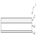
- 기재 필름의 한 쪽의 면에 마찰 저감제 및 대전 방지제를 함유하는 배면층을 가지고, 다른 한 쪽의 면에 점착제층을 가지는 레이저 다이싱용 점착 시트로서,
상기 배면층의 표면의 산술평균 조도 Ra가 0.1μm 이하이며,
상기 점착 시트의 23℃에서의 인장 탄성율이 50~200MPa이며,
400~1400nm의 파장영역에서의 평행선 투과율이 85% 이상인,
레이저 다이싱용 점착 시트. - 제1항에 있어서,
상기 마찰 저감제가 실리콘계 그라프트 공중합체인 레이저 다이싱용 점착 시트. - 제1항 또는 제2항에 있어서,
상기 대전 방지제가 4급 아민염 단량체인 레이저 다이싱용 점착 시트. - 제1항 ~ 제3항 중 어느 한 항에 있어서,
상기 배면층에는, 유기 바인더 100질량부, 대전 방지제 0.005~10질량부 및 마찰 저감제 0.005~10질량부가 함유되는 레이저 다이싱용 점착 시트. - 제4항에 있어서,
상기 유기 바인더가 (메트)아크릴산에스테르 공중합체인 레이저 다이싱용 점착 시트. - 표면에 회로가 형성된 반도체 웨이퍼의 이면 또는 표면에, 제1항 ~ 제5항 중 어느 한 항에 기재된 레이저 다이싱용 점착 시트를 첩부하는 공정과,
상기 점착 시트 너머로, 상기 반도체 웨이퍼에 가시영역의 파장의 레이저광을 조사하여 웨이퍼의 위치 정합을 실시하는 공정과,
상기 점착 시트 너머로, 상기 반도체 웨이퍼에 적외영역의 파장의 레이저광을 조사하여 웨이퍼 내부에 개질부를 형성하는 공정과,
상기 점착 시트의 익스팬드에 의해, 상기 반도체 웨이퍼를 분할하여 칩화하는 공정,
을 포함하는 반도체 장치의 제조 방법.
Applications Claiming Priority (3)
| Application Number | Priority Date | Filing Date | Title |
|---|---|---|---|
| JP2014261750 | 2014-12-25 | ||
| JPJP-P-2014-261750 | 2014-12-25 | ||
| PCT/JP2015/080289 WO2016103902A1 (ja) | 2014-12-25 | 2015-10-27 | レーザーダイシング用粘着シートおよび半導体装置の製造方法 |
Publications (2)
| Publication Number | Publication Date |
|---|---|
| KR20170100543A true KR20170100543A (ko) | 2017-09-04 |
| KR102430472B1 KR102430472B1 (ko) | 2022-08-05 |
Family
ID=56149938
Family Applications (1)
| Application Number | Title | Priority Date | Filing Date |
|---|---|---|---|
| KR1020177018400A Active KR102430472B1 (ko) | 2014-12-25 | 2015-10-27 | 레이저 다이싱용 점착 시트 및 반도체 장치의 제조 방법 |
Country Status (7)
| Country | Link |
|---|---|
| US (1) | US10008406B2 (ko) |
| JP (1) | JP6545712B2 (ko) |
| KR (1) | KR102430472B1 (ko) |
| CN (1) | CN107148663B (ko) |
| SG (1) | SG11201705157WA (ko) |
| TW (1) | TWI684211B (ko) |
| WO (1) | WO2016103902A1 (ko) |
Cited By (1)
| Publication number | Priority date | Publication date | Assignee | Title |
|---|---|---|---|---|
| KR20230014687A (ko) * | 2020-05-21 | 2023-01-30 | 덴카 주식회사 | 조성물 |
Families Citing this family (15)
| Publication number | Priority date | Publication date | Assignee | Title |
|---|---|---|---|---|
| US10429892B1 (en) | 2016-01-12 | 2019-10-01 | Apple Inc. | Electronic devices with thin display housings |
| JP6886831B2 (ja) * | 2017-02-10 | 2021-06-16 | デンカ株式会社 | 粘着シート及びそれを用いた半導体チップ又は半導体部品の製造方法 |
| JP2018181901A (ja) * | 2017-04-04 | 2018-11-15 | 株式会社ディスコ | 加工方法 |
| JP6832784B2 (ja) * | 2017-04-24 | 2021-02-24 | デンカ株式会社 | ステルスダイシング用粘着テープ及びそれを用いた半導体チップの製造方法 |
| JP7025138B2 (ja) * | 2017-06-15 | 2022-02-24 | 三井化学東セロ株式会社 | 粘着性積層フィルムおよび電子装置の製造方法 |
| JP7159186B2 (ja) * | 2017-10-27 | 2022-10-24 | リンテック株式会社 | 保護膜形成用複合シート、及び半導体チップの製造方法 |
| JP7015166B2 (ja) * | 2017-12-28 | 2022-02-02 | 日東電工株式会社 | ダイシングテープ一体型半導体背面密着フィルム |
| KR102637162B1 (ko) * | 2018-06-12 | 2024-02-16 | 도쿄엘렉트론가부시키가이샤 | 기판 처리 방법, 개질 장치 및 기판 처리 시스템 |
| JP7497297B2 (ja) * | 2018-12-05 | 2024-06-10 | リンテック株式会社 | 保護膜形成用複合シート、及び半導体チップの製造方法 |
| CN113169059A (zh) * | 2018-12-05 | 2021-07-23 | 琳得科株式会社 | 保护膜形成用复合片及半导体芯片的制造方法 |
| KR102833268B1 (ko) * | 2019-06-19 | 2025-07-10 | 가부시끼가이샤 레조낙 | 반도체 밀봉 성형용 임시 보호 필름, 임시 보호 필름 부착 리드 프레임, 임시 보호 필름 부착 밀봉 성형체, 및 반도체 장치를 제조하는 방법 |
| CN111785952B (zh) * | 2020-01-19 | 2021-10-29 | 成都拓米电子装备制造有限公司 | 一种二次电池负极材料用纳米硅粒子的制造方法 |
| US12552975B2 (en) | 2020-03-06 | 2026-02-17 | Tredegar Surface Protection, Llc | Carrier film for semi-conductor wafer processing |
| JP2025126750A (ja) * | 2024-02-19 | 2025-08-29 | デンカ株式会社 | ダイシングテープ及びウェハ加工方法 |
| WO2025197708A1 (ja) * | 2024-03-22 | 2025-09-25 | グンゼ株式会社 | 基材フィルム |
Citations (5)
| Publication number | Priority date | Publication date | Assignee | Title |
|---|---|---|---|---|
| JP3762409B2 (ja) | 2002-03-12 | 2006-04-05 | 浜松ホトニクス株式会社 | 基板の分割方法 |
| JP2009013183A (ja) * | 2005-12-07 | 2009-01-22 | Denki Kagaku Kogyo Kk | 粘着シート及びそれを用いた電子部品製造方法。 |
| JP2011139042A (ja) | 2009-12-04 | 2011-07-14 | Lintec Corp | ステルスダイシング用粘着シート及び半導体装置の製造方法 |
| JP2012015236A (ja) * | 2010-06-30 | 2012-01-19 | Furukawa Electric Co Ltd:The | ウエハ貼着用粘着シートおよびそれを用いたウエハの加工方法 |
| JP2014152241A (ja) * | 2013-02-08 | 2014-08-25 | Nitto Denko Corp | 粘着テープ |
Family Cites Families (15)
| Publication number | Priority date | Publication date | Assignee | Title |
|---|---|---|---|---|
| JP2000080135A (ja) * | 1998-09-02 | 2000-03-21 | Toagosei Co Ltd | グラフト共重合体の製造方法 |
| JP3795040B2 (ja) * | 2003-12-03 | 2006-07-12 | 沖電気工業株式会社 | 半導体装置の製造方法 |
| US7622185B2 (en) * | 2005-04-15 | 2009-11-24 | Nitto Denko Corporation | Protective cover sheet comprising a UV-absorbing layer for a polarizer plate and method of making the same |
| JP4024263B2 (ja) * | 2005-10-06 | 2007-12-19 | 電気化学工業株式会社 | 粘着シート及びそれを用いた電子部品製造方法。 |
| JP4861081B2 (ja) * | 2006-07-14 | 2012-01-25 | 電気化学工業株式会社 | 半導体部材固定用粘着シート及びそれを用いた電子部品製造方法。 |
| WO2011065252A1 (ja) * | 2009-11-30 | 2011-06-03 | 電気化学工業株式会社 | 粘着シート及び電子部品 |
| JP5128575B2 (ja) * | 2009-12-04 | 2013-01-23 | リンテック株式会社 | ステルスダイシング用粘着シート及び半導体装置の製造方法 |
| KR101282707B1 (ko) * | 2009-12-30 | 2013-07-05 | 제일모직주식회사 | 코어-쉘 구조를 포함하는 그라프트 공중합체로 이루어지는 실리콘계 충격보강제 및 이를 포함하는 열가소성 조성물 |
| JP5955579B2 (ja) * | 2011-07-21 | 2016-07-20 | 日東電工株式会社 | ガラスエッチング用保護シート |
| WO2014069638A1 (ja) * | 2012-11-05 | 2014-05-08 | リンテック株式会社 | 粘着シート |
| WO2015174381A1 (ja) * | 2014-05-12 | 2015-11-19 | 電気化学工業株式会社 | 半導体検査用の耐熱性粘着シート、及び半導体検査方法 |
| US9165832B1 (en) * | 2014-06-30 | 2015-10-20 | Applied Materials, Inc. | Method of die singulation using laser ablation and induction of internal defects with a laser |
| KR102360607B1 (ko) * | 2014-07-14 | 2022-02-08 | 덴카 주식회사 | 점착 시트, 전자 부품의 제조 방법 |
| KR102457313B1 (ko) * | 2014-09-29 | 2022-10-20 | 린텍 가부시키가이샤 | 반도체 웨이퍼 가공용 시트용 기재, 반도체 웨이퍼 가공용 시트 및 반도체 장치의 제조 방법 |
| SG11201704347YA (en) * | 2014-12-02 | 2017-06-29 | Lintec Corp | Adhesive sheet, and method for manufacturing processed article |
-
2015
- 2015-10-27 KR KR1020177018400A patent/KR102430472B1/ko active Active
- 2015-10-27 SG SG11201705157WA patent/SG11201705157WA/en unknown
- 2015-10-27 US US15/539,626 patent/US10008406B2/en active Active
- 2015-10-27 WO PCT/JP2015/080289 patent/WO2016103902A1/ja not_active Ceased
- 2015-10-27 CN CN201580066761.XA patent/CN107148663B/zh active Active
- 2015-10-27 JP JP2016565994A patent/JP6545712B2/ja active Active
- 2015-12-11 TW TW104141643A patent/TWI684211B/zh active
Patent Citations (6)
| Publication number | Priority date | Publication date | Assignee | Title |
|---|---|---|---|---|
| JP3762409B2 (ja) | 2002-03-12 | 2006-04-05 | 浜松ホトニクス株式会社 | 基板の分割方法 |
| JP2009013183A (ja) * | 2005-12-07 | 2009-01-22 | Denki Kagaku Kogyo Kk | 粘着シート及びそれを用いた電子部品製造方法。 |
| JP2011139042A (ja) | 2009-12-04 | 2011-07-14 | Lintec Corp | ステルスダイシング用粘着シート及び半導体装置の製造方法 |
| JP2012015236A (ja) * | 2010-06-30 | 2012-01-19 | Furukawa Electric Co Ltd:The | ウエハ貼着用粘着シートおよびそれを用いたウエハの加工方法 |
| JP5391158B2 (ja) | 2010-06-30 | 2014-01-15 | 古河電気工業株式会社 | ウエハ貼着用粘着シートおよびそれを用いたウエハの加工方法 |
| JP2014152241A (ja) * | 2013-02-08 | 2014-08-25 | Nitto Denko Corp | 粘着テープ |
Cited By (2)
| Publication number | Priority date | Publication date | Assignee | Title |
|---|---|---|---|---|
| KR20230014687A (ko) * | 2020-05-21 | 2023-01-30 | 덴카 주식회사 | 조성물 |
| US12480025B2 (en) | 2020-05-21 | 2025-11-25 | Denka Company Limited | Composition |
Also Published As
| Publication number | Publication date |
|---|---|
| US10008406B2 (en) | 2018-06-26 |
| JPWO2016103902A1 (ja) | 2017-11-24 |
| US20170365500A1 (en) | 2017-12-21 |
| TWI684211B (zh) | 2020-02-01 |
| CN107148663A (zh) | 2017-09-08 |
| SG11201705157WA (en) | 2017-07-28 |
| TW201635359A (zh) | 2016-10-01 |
| JP6545712B2 (ja) | 2019-07-17 |
| CN107148663B (zh) | 2020-11-06 |
| KR102430472B1 (ko) | 2022-08-05 |
| WO2016103902A1 (ja) | 2016-06-30 |
Similar Documents
| Publication | Publication Date | Title |
|---|---|---|
| KR102430472B1 (ko) | 레이저 다이싱용 점착 시트 및 반도체 장치의 제조 방법 | |
| JP6475901B2 (ja) | 半導体加工用粘着テープおよび半導体装置の製造方法 | |
| TWI625244B (zh) | 附雙面黏著劑之光學薄膜、及使用其之圖像顯示裝置之製造方法 | |
| JP7326270B2 (ja) | 半導体加工用粘着テープおよび半導体装置の製造方法 | |
| KR101215105B1 (ko) | 스텔스 다이싱용 점착 시트 및 반도체 장치의 제조 방법 | |
| CN102473617B (zh) | 晶片粘贴用粘合片及使用该粘合片的晶片的加工方法 | |
| WO2020003919A1 (ja) | 半導体加工用粘着テープおよび半導体装置の製造方法 | |
| KR101023368B1 (ko) | 수지 조성물 및 그것을 이용하는 피가공 부재의 가고정 방법과 표면 보호 방법 | |
| KR101643793B1 (ko) | 점착제 및 점착 시트 | |
| TWI642547B (zh) | 積層體、半導體用表面保護膜、半導體裝置的製造方法及樹脂改質劑 | |
| KR102360607B1 (ko) | 점착 시트, 전자 부품의 제조 방법 | |
| JP2011139042A (ja) | ステルスダイシング用粘着シート及び半導体装置の製造方法 | |
| JP6375081B2 (ja) | 半導体加工用粘着テープ、及び半導体装置の製造方法 | |
| CN108207116B (zh) | 半导体加工用粘合片 | |
| TW202113016A (zh) | 光交聯性黏著劑及其利用 | |
| TWI704208B (zh) | 半導體加工用黏合膠帶和使用該膠帶的半導體晶片或半導體部件的製造方法 | |
| JP2011077235A (ja) | 素子保持用粘着シートおよび素子の製造方法 | |
| JP6616558B1 (ja) | 半導体加工用粘着テープおよび半導体装置の製造方法 | |
| JP7850802B2 (ja) | 半導体加工用粘着テープ |
Legal Events
| Date | Code | Title | Description |
|---|---|---|---|
| PA0105 | International application |
St.27 status event code: A-0-1-A10-A15-nap-PA0105 |
|
| PG1501 | Laying open of application |
St.27 status event code: A-1-1-Q10-Q12-nap-PG1501 |
|
| P22-X000 | Classification modified |
St.27 status event code: A-2-2-P10-P22-nap-X000 |
|
| P22-X000 | Classification modified |
St.27 status event code: A-2-2-P10-P22-nap-X000 |
|
| P22-X000 | Classification modified |
St.27 status event code: A-2-2-P10-P22-nap-X000 |
|
| A201 | Request for examination | ||
| PA0201 | Request for examination |
St.27 status event code: A-1-2-D10-D11-exm-PA0201 |
|
| E902 | Notification of reason for refusal | ||
| PE0902 | Notice of grounds for rejection |
St.27 status event code: A-1-2-D10-D21-exm-PE0902 |
|
| P11-X000 | Amendment of application requested |
St.27 status event code: A-2-2-P10-P11-nap-X000 |
|
| P13-X000 | Application amended |
St.27 status event code: A-2-2-P10-P13-nap-X000 |
|
| E701 | Decision to grant or registration of patent right | ||
| PE0701 | Decision of registration |
St.27 status event code: A-1-2-D10-D22-exm-PE0701 |
|
| GRNT | Written decision to grant | ||
| PR0701 | Registration of establishment |
St.27 status event code: A-2-4-F10-F11-exm-PR0701 |
|
| PR1002 | Payment of registration fee |
St.27 status event code: A-2-2-U10-U12-oth-PR1002 Fee payment year number: 1 |
|
| PG1601 | Publication of registration |
St.27 status event code: A-4-4-Q10-Q13-nap-PG1601 |
|
| P22-X000 | Classification modified |
St.27 status event code: A-4-4-P10-P22-nap-X000 |