KR20170101276A - 소결가능한 접착 재료 및 그것을 사용한 반도체 디바이스 - Google Patents
소결가능한 접착 재료 및 그것을 사용한 반도체 디바이스 Download PDFInfo
- Publication number
- KR20170101276A KR20170101276A KR1020177020657A KR20177020657A KR20170101276A KR 20170101276 A KR20170101276 A KR 20170101276A KR 1020177020657 A KR1020177020657 A KR 1020177020657A KR 20177020657 A KR20177020657 A KR 20177020657A KR 20170101276 A KR20170101276 A KR 20170101276A
- Authority
- KR
- South Korea
- Prior art keywords
- adhesive material
- filler
- less
- silver
- resin particles
- Prior art date
- Legal status (The legal status is an assumption and is not a legal conclusion. Google has not performed a legal analysis and makes no representation as to the accuracy of the status listed.)
- Granted
Links
Images

Classifications
-
- B—PERFORMING OPERATIONS; TRANSPORTING
- B22—CASTING; POWDER METALLURGY
- B22F—WORKING METALLIC POWDER; MANUFACTURE OF ARTICLES FROM METALLIC POWDER; MAKING METALLIC POWDER; APPARATUS OR DEVICES SPECIALLY ADAPTED FOR METALLIC POWDER
- B22F3/00—Manufacture of workpieces or articles from metallic powder characterised by the manner of compacting or sintering; Apparatus specially adapted therefor ; Presses and furnaces
- B22F3/22—Manufacture of workpieces or articles from metallic powder characterised by the manner of compacting or sintering; Apparatus specially adapted therefor ; Presses and furnaces for producing castings from a slip
-
- C—CHEMISTRY; METALLURGY
- C09—DYES; PAINTS; POLISHES; NATURAL RESINS; ADHESIVES; COMPOSITIONS NOT OTHERWISE PROVIDED FOR; APPLICATIONS OF MATERIALS NOT OTHERWISE PROVIDED FOR
- C09J—ADHESIVES; NON-MECHANICAL ASPECTS OF ADHESIVE PROCESSES IN GENERAL; ADHESIVE PROCESSES NOT PROVIDED FOR ELSEWHERE; USE OF MATERIALS AS ADHESIVES
- C09J11/00—Features of adhesives not provided for in group C09J9/00, e.g. additives
- C09J11/02—Non-macromolecular additives
- C09J11/04—Non-macromolecular additives inorganic
-
- B—PERFORMING OPERATIONS; TRANSPORTING
- B22—CASTING; POWDER METALLURGY
- B22F—WORKING METALLIC POWDER; MANUFACTURE OF ARTICLES FROM METALLIC POWDER; MAKING METALLIC POWDER; APPARATUS OR DEVICES SPECIALLY ADAPTED FOR METALLIC POWDER
- B22F1/00—Metallic powder; Treatment of metallic powder, e.g. to facilitate working or to improve properties
- B22F1/06—Metallic powder characterised by the shape of the particles
- B22F1/068—Flake-like particles
-
- B—PERFORMING OPERATIONS; TRANSPORTING
- B22—CASTING; POWDER METALLURGY
- B22F—WORKING METALLIC POWDER; MANUFACTURE OF ARTICLES FROM METALLIC POWDER; MAKING METALLIC POWDER; APPARATUS OR DEVICES SPECIALLY ADAPTED FOR METALLIC POWDER
- B22F1/00—Metallic powder; Treatment of metallic powder, e.g. to facilitate working or to improve properties
- B22F1/10—Metallic powder containing lubricating or binding agents; Metallic powder containing organic material
-
- B—PERFORMING OPERATIONS; TRANSPORTING
- B22—CASTING; POWDER METALLURGY
- B22F—WORKING METALLIC POWDER; MANUFACTURE OF ARTICLES FROM METALLIC POWDER; MAKING METALLIC POWDER; APPARATUS OR DEVICES SPECIALLY ADAPTED FOR METALLIC POWDER
- B22F1/00—Metallic powder; Treatment of metallic powder, e.g. to facilitate working or to improve properties
- B22F1/10—Metallic powder containing lubricating or binding agents; Metallic powder containing organic material
- B22F1/107—Metallic powder containing lubricating or binding agents; Metallic powder containing organic material containing organic material comprising solvents, e.g. for slip casting
-
- B—PERFORMING OPERATIONS; TRANSPORTING
- B22—CASTING; POWDER METALLURGY
- B22F—WORKING METALLIC POWDER; MANUFACTURE OF ARTICLES FROM METALLIC POWDER; MAKING METALLIC POWDER; APPARATUS OR DEVICES SPECIALLY ADAPTED FOR METALLIC POWDER
- B22F7/00—Manufacture of composite layers, workpieces, or articles, comprising metallic powder, by sintering the powder, with or without compacting wherein at least one part is obtained by sintering or compression
- B22F7/02—Manufacture of composite layers, workpieces, or articles, comprising metallic powder, by sintering the powder, with or without compacting wherein at least one part is obtained by sintering or compression of composite layers
- B22F7/04—Manufacture of composite layers, workpieces, or articles, comprising metallic powder, by sintering the powder, with or without compacting wherein at least one part is obtained by sintering or compression of composite layers with one or more layers not made from powder, e.g. made from solid metal
-
- B—PERFORMING OPERATIONS; TRANSPORTING
- B22—CASTING; POWDER METALLURGY
- B22F—WORKING METALLIC POWDER; MANUFACTURE OF ARTICLES FROM METALLIC POWDER; MAKING METALLIC POWDER; APPARATUS OR DEVICES SPECIALLY ADAPTED FOR METALLIC POWDER
- B22F7/00—Manufacture of composite layers, workpieces, or articles, comprising metallic powder, by sintering the powder, with or without compacting wherein at least one part is obtained by sintering or compression
- B22F7/06—Manufacture of composite layers, workpieces, or articles, comprising metallic powder, by sintering the powder, with or without compacting wherein at least one part is obtained by sintering or compression of composite workpieces or articles from parts, e.g. to form tipped tools
- B22F7/08—Manufacture of composite layers, workpieces, or articles, comprising metallic powder, by sintering the powder, with or without compacting wherein at least one part is obtained by sintering or compression of composite workpieces or articles from parts, e.g. to form tipped tools with one or more parts not made from powder
-
- B—PERFORMING OPERATIONS; TRANSPORTING
- B23—MACHINE TOOLS; METAL-WORKING NOT OTHERWISE PROVIDED FOR
- B23K—SOLDERING OR UNSOLDERING; WELDING; CLADDING OR PLATING BY SOLDERING OR WELDING; CUTTING BY APPLYING HEAT LOCALLY, e.g. FLAME CUTTING; WORKING BY LASER BEAM
- B23K35/00—Rods, electrodes, materials, or media, for use in soldering, welding, or cutting
- B23K35/02—Rods, electrodes, materials, or media, for use in soldering, welding, or cutting characterised by mechanical features, e.g. shape
- B23K35/0222—Rods, electrodes, materials, or media, for use in soldering, welding, or cutting characterised by mechanical features, e.g. shape for use in soldering or brazing
- B23K35/0244—Powders, particles or spheres; Preforms made therefrom
-
- C—CHEMISTRY; METALLURGY
- C09—DYES; PAINTS; POLISHES; NATURAL RESINS; ADHESIVES; COMPOSITIONS NOT OTHERWISE PROVIDED FOR; APPLICATIONS OF MATERIALS NOT OTHERWISE PROVIDED FOR
- C09J—ADHESIVES; NON-MECHANICAL ASPECTS OF ADHESIVE PROCESSES IN GENERAL; ADHESIVE PROCESSES NOT PROVIDED FOR ELSEWHERE; USE OF MATERIALS AS ADHESIVES
- C09J115/00—Adhesives based on rubber derivatives
- C09J115/02—Rubber derivatives containing halogen
-
- C—CHEMISTRY; METALLURGY
- C09—DYES; PAINTS; POLISHES; NATURAL RESINS; ADHESIVES; COMPOSITIONS NOT OTHERWISE PROVIDED FOR; APPLICATIONS OF MATERIALS NOT OTHERWISE PROVIDED FOR
- C09J—ADHESIVES; NON-MECHANICAL ASPECTS OF ADHESIVE PROCESSES IN GENERAL; ADHESIVE PROCESSES NOT PROVIDED FOR ELSEWHERE; USE OF MATERIALS AS ADHESIVES
- C09J5/00—Adhesive processes in general; Adhesive processes not provided for elsewhere, e.g. relating to primers
- C09J5/06—Adhesive processes in general; Adhesive processes not provided for elsewhere, e.g. relating to primers involving heating of the applied adhesive
-
- H01L21/185—
-
- H01L24/29—
-
- H—ELECTRICITY
- H10—SEMICONDUCTOR DEVICES; ELECTRIC SOLID-STATE DEVICES NOT OTHERWISE PROVIDED FOR
- H10P—GENERIC PROCESSES OR APPARATUS FOR THE MANUFACTURE OR TREATMENT OF DEVICES COVERED BY CLASS H10
- H10P10/00—Bonding of wafers, substrates or parts of devices
- H10P10/12—Bonding of semiconductor wafers or semiconductor substrates to semiconductor wafers or semiconductor substrates
-
- H—ELECTRICITY
- H10—SEMICONDUCTOR DEVICES; ELECTRIC SOLID-STATE DEVICES NOT OTHERWISE PROVIDED FOR
- H10W—GENERIC PACKAGES, INTERCONNECTIONS, CONNECTORS OR OTHER CONSTRUCTIONAL DETAILS OF DEVICES COVERED BY CLASS H10
- H10W72/00—Interconnections or connectors in packages
- H10W72/30—Die-attach connectors
-
- B—PERFORMING OPERATIONS; TRANSPORTING
- B22—CASTING; POWDER METALLURGY
- B22F—WORKING METALLIC POWDER; MANUFACTURE OF ARTICLES FROM METALLIC POWDER; MAKING METALLIC POWDER; APPARATUS OR DEVICES SPECIALLY ADAPTED FOR METALLIC POWDER
- B22F7/00—Manufacture of composite layers, workpieces, or articles, comprising metallic powder, by sintering the powder, with or without compacting wherein at least one part is obtained by sintering or compression
- B22F7/02—Manufacture of composite layers, workpieces, or articles, comprising metallic powder, by sintering the powder, with or without compacting wherein at least one part is obtained by sintering or compression of composite layers
- B22F7/04—Manufacture of composite layers, workpieces, or articles, comprising metallic powder, by sintering the powder, with or without compacting wherein at least one part is obtained by sintering or compression of composite layers with one or more layers not made from powder, e.g. made from solid metal
- B22F2007/042—Manufacture of composite layers, workpieces, or articles, comprising metallic powder, by sintering the powder, with or without compacting wherein at least one part is obtained by sintering or compression of composite layers with one or more layers not made from powder, e.g. made from solid metal characterised by the layer forming method
- B22F2007/047—Manufacture of composite layers, workpieces, or articles, comprising metallic powder, by sintering the powder, with or without compacting wherein at least one part is obtained by sintering or compression of composite layers with one or more layers not made from powder, e.g. made from solid metal characterised by the layer forming method non-pressurised baking of the paste or slurry containing metal powder
-
- B—PERFORMING OPERATIONS; TRANSPORTING
- B22—CASTING; POWDER METALLURGY
- B22F—WORKING METALLIC POWDER; MANUFACTURE OF ARTICLES FROM METALLIC POWDER; MAKING METALLIC POWDER; APPARATUS OR DEVICES SPECIALLY ADAPTED FOR METALLIC POWDER
- B22F7/00—Manufacture of composite layers, workpieces, or articles, comprising metallic powder, by sintering the powder, with or without compacting wherein at least one part is obtained by sintering or compression
- B22F7/06—Manufacture of composite layers, workpieces, or articles, comprising metallic powder, by sintering the powder, with or without compacting wherein at least one part is obtained by sintering or compression of composite workpieces or articles from parts, e.g. to form tipped tools
- B22F7/062—Manufacture of composite layers, workpieces, or articles, comprising metallic powder, by sintering the powder, with or without compacting wherein at least one part is obtained by sintering or compression of composite workpieces or articles from parts, e.g. to form tipped tools involving the connection or repairing of preformed parts
- B22F7/064—Manufacture of composite layers, workpieces, or articles, comprising metallic powder, by sintering the powder, with or without compacting wherein at least one part is obtained by sintering or compression of composite workpieces or articles from parts, e.g. to form tipped tools involving the connection or repairing of preformed parts using an intermediate powder layer
-
- C09J2201/622—
-
- C—CHEMISTRY; METALLURGY
- C09—DYES; PAINTS; POLISHES; NATURAL RESINS; ADHESIVES; COMPOSITIONS NOT OTHERWISE PROVIDED FOR; APPLICATIONS OF MATERIALS NOT OTHERWISE PROVIDED FOR
- C09J—ADHESIVES; NON-MECHANICAL ASPECTS OF ADHESIVE PROCESSES IN GENERAL; ADHESIVE PROCESSES NOT PROVIDED FOR ELSEWHERE; USE OF MATERIALS AS ADHESIVES
- C09J2203/00—Applications of adhesives in processes or use of adhesives in the form of films or foils
- C09J2203/326—Applications of adhesives in processes or use of adhesives in the form of films or foils for bonding electronic components such as wafers, chips or semiconductors
-
- C—CHEMISTRY; METALLURGY
- C09—DYES; PAINTS; POLISHES; NATURAL RESINS; ADHESIVES; COMPOSITIONS NOT OTHERWISE PROVIDED FOR; APPLICATIONS OF MATERIALS NOT OTHERWISE PROVIDED FOR
- C09J—ADHESIVES; NON-MECHANICAL ASPECTS OF ADHESIVE PROCESSES IN GENERAL; ADHESIVE PROCESSES NOT PROVIDED FOR ELSEWHERE; USE OF MATERIALS AS ADHESIVES
- C09J2301/00—Additional features of adhesives in the form of films or foils
- C09J2301/30—Additional features of adhesives in the form of films or foils characterized by the chemical, physicochemical or physical properties of the adhesive or the carrier
- C09J2301/312—Additional features of adhesives in the form of films or foils characterized by the chemical, physicochemical or physical properties of the adhesive or the carrier parameters being the characterizing feature
-
- H01L2224/04026—
-
- H01L2224/05639—
-
- H—ELECTRICITY
- H05—ELECTRIC TECHNIQUES NOT OTHERWISE PROVIDED FOR
- H05K—PRINTED CIRCUITS; CASINGS OR CONSTRUCTIONAL DETAILS OF ELECTRIC APPARATUS; MANUFACTURE OF ASSEMBLAGES OF ELECTRICAL COMPONENTS
- H05K2203/00—Indexing scheme relating to apparatus or processes for manufacturing printed circuits covered by H05K3/00
- H05K2203/11—Treatments characterised by their effect, e.g. heating, cooling, roughening
- H05K2203/1131—Sintering, i.e. fusing of metal particles to achieve or improve electrical conductivity
-
- H—ELECTRICITY
- H05—ELECTRIC TECHNIQUES NOT OTHERWISE PROVIDED FOR
- H05K—PRINTED CIRCUITS; CASINGS OR CONSTRUCTIONAL DETAILS OF ELECTRIC APPARATUS; MANUFACTURE OF ASSEMBLAGES OF ELECTRICAL COMPONENTS
- H05K3/00—Apparatus or processes for manufacturing printed circuits
- H05K3/30—Assembling printed circuits with electric components, e.g. with resistors
- H05K3/32—Assembling printed circuits with electric components, e.g. with resistors electrically connecting electric components or wires to printed circuits
-
- H—ELECTRICITY
- H10—SEMICONDUCTOR DEVICES; ELECTRIC SOLID-STATE DEVICES NOT OTHERWISE PROVIDED FOR
- H10W—GENERIC PACKAGES, INTERCONNECTIONS, CONNECTORS OR OTHER CONSTRUCTIONAL DETAILS OF DEVICES COVERED BY CLASS H10
- H10W72/00—Interconnections or connectors in packages
- H10W72/071—Connecting or disconnecting
- H10W72/073—Connecting or disconnecting of die-attach connectors
- H10W72/07331—Connecting techniques
-
- H—ELECTRICITY
- H10—SEMICONDUCTOR DEVICES; ELECTRIC SOLID-STATE DEVICES NOT OTHERWISE PROVIDED FOR
- H10W—GENERIC PACKAGES, INTERCONNECTIONS, CONNECTORS OR OTHER CONSTRUCTIONAL DETAILS OF DEVICES COVERED BY CLASS H10
- H10W72/00—Interconnections or connectors in packages
- H10W72/071—Connecting or disconnecting
- H10W72/073—Connecting or disconnecting of die-attach connectors
- H10W72/07331—Connecting techniques
- H10W72/07335—Applying EM radiation, e.g. induction heating or using a laser
-
- H—ELECTRICITY
- H10—SEMICONDUCTOR DEVICES; ELECTRIC SOLID-STATE DEVICES NOT OTHERWISE PROVIDED FOR
- H10W—GENERIC PACKAGES, INTERCONNECTIONS, CONNECTORS OR OTHER CONSTRUCTIONAL DETAILS OF DEVICES COVERED BY CLASS H10
- H10W72/00—Interconnections or connectors in packages
- H10W72/30—Die-attach connectors
- H10W72/321—Structures or relative sizes of die-attach connectors
- H10W72/325—Die-attach connectors having a filler embedded in a matrix
-
- H—ELECTRICITY
- H10—SEMICONDUCTOR DEVICES; ELECTRIC SOLID-STATE DEVICES NOT OTHERWISE PROVIDED FOR
- H10W—GENERIC PACKAGES, INTERCONNECTIONS, CONNECTORS OR OTHER CONSTRUCTIONAL DETAILS OF DEVICES COVERED BY CLASS H10
- H10W72/00—Interconnections or connectors in packages
- H10W72/30—Die-attach connectors
- H10W72/351—Materials of die-attach connectors
-
- H—ELECTRICITY
- H10—SEMICONDUCTOR DEVICES; ELECTRIC SOLID-STATE DEVICES NOT OTHERWISE PROVIDED FOR
- H10W—GENERIC PACKAGES, INTERCONNECTIONS, CONNECTORS OR OTHER CONSTRUCTIONAL DETAILS OF DEVICES COVERED BY CLASS H10
- H10W72/00—Interconnections or connectors in packages
- H10W72/30—Die-attach connectors
- H10W72/351—Materials of die-attach connectors
- H10W72/352—Materials of die-attach connectors comprising metals or metalloids, e.g. solders
-
- H—ELECTRICITY
- H10—SEMICONDUCTOR DEVICES; ELECTRIC SOLID-STATE DEVICES NOT OTHERWISE PROVIDED FOR
- H10W—GENERIC PACKAGES, INTERCONNECTIONS, CONNECTORS OR OTHER CONSTRUCTIONAL DETAILS OF DEVICES COVERED BY CLASS H10
- H10W72/00—Interconnections or connectors in packages
- H10W72/30—Die-attach connectors
- H10W72/351—Materials of die-attach connectors
- H10W72/353—Materials of die-attach connectors not comprising solid metals or solid metalloids, e.g. ceramics
- H10W72/354—Materials of die-attach connectors not comprising solid metals or solid metalloids, e.g. ceramics comprising polymers
-
- H—ELECTRICITY
- H10—SEMICONDUCTOR DEVICES; ELECTRIC SOLID-STATE DEVICES NOT OTHERWISE PROVIDED FOR
- H10W—GENERIC PACKAGES, INTERCONNECTIONS, CONNECTORS OR OTHER CONSTRUCTIONAL DETAILS OF DEVICES COVERED BY CLASS H10
- H10W72/00—Interconnections or connectors in packages
- H10W72/30—Die-attach connectors
- H10W72/351—Materials of die-attach connectors
- H10W72/355—Materials of die-attach connectors of outermost layers of multilayered die-attach connectors, e.g. material of a coating
-
- H—ELECTRICITY
- H10—SEMICONDUCTOR DEVICES; ELECTRIC SOLID-STATE DEVICES NOT OTHERWISE PROVIDED FOR
- H10W—GENERIC PACKAGES, INTERCONNECTIONS, CONNECTORS OR OTHER CONSTRUCTIONAL DETAILS OF DEVICES COVERED BY CLASS H10
- H10W72/00—Interconnections or connectors in packages
- H10W72/50—Bond wires
- H10W72/59—Bond pads specially adapted therefor
-
- H—ELECTRICITY
- H10—SEMICONDUCTOR DEVICES; ELECTRIC SOLID-STATE DEVICES NOT OTHERWISE PROVIDED FOR
- H10W—GENERIC PACKAGES, INTERCONNECTIONS, CONNECTORS OR OTHER CONSTRUCTIONAL DETAILS OF DEVICES COVERED BY CLASS H10
- H10W72/00—Interconnections or connectors in packages
- H10W72/90—Bond pads, in general
- H10W72/951—Materials of bond pads
- H10W72/952—Materials of bond pads comprising metals or metalloids, e.g. PbSn, Ag or Cu
-
- H—ELECTRICITY
- H10—SEMICONDUCTOR DEVICES; ELECTRIC SOLID-STATE DEVICES NOT OTHERWISE PROVIDED FOR
- H10W—GENERIC PACKAGES, INTERCONNECTIONS, CONNECTORS OR OTHER CONSTRUCTIONAL DETAILS OF DEVICES COVERED BY CLASS H10
- H10W90/00—Package configurations
- H10W90/701—Package configurations characterised by the relative positions of pads or connectors relative to package parts
- H10W90/731—Package configurations characterised by the relative positions of pads or connectors relative to package parts of die-attach connectors
- H10W90/734—Package configurations characterised by the relative positions of pads or connectors relative to package parts of die-attach connectors between a chip and a stacked insulating package substrate, interposer or RDL
-
- H—ELECTRICITY
- H10—SEMICONDUCTOR DEVICES; ELECTRIC SOLID-STATE DEVICES NOT OTHERWISE PROVIDED FOR
- H10W—GENERIC PACKAGES, INTERCONNECTIONS, CONNECTORS OR OTHER CONSTRUCTIONAL DETAILS OF DEVICES COVERED BY CLASS H10
- H10W90/00—Package configurations
- H10W90/701—Package configurations characterised by the relative positions of pads or connectors relative to package parts
- H10W90/731—Package configurations characterised by the relative positions of pads or connectors relative to package parts of die-attach connectors
- H10W90/736—Package configurations characterised by the relative positions of pads or connectors relative to package parts of die-attach connectors between a chip and a stacked lead frame, conducting package substrate or heat sink
Landscapes
- Chemical & Material Sciences (AREA)
- Engineering & Computer Science (AREA)
- Mechanical Engineering (AREA)
- Manufacturing & Machinery (AREA)
- Composite Materials (AREA)
- Materials Engineering (AREA)
- Organic Chemistry (AREA)
- Nanotechnology (AREA)
- Inorganic Chemistry (AREA)
- Powder Metallurgy (AREA)
- Die Bonding (AREA)
- Adhesives Or Adhesive Processes (AREA)
- Conductive Materials (AREA)
- Electric Connection Of Electric Components To Printed Circuits (AREA)
Abstract
Description
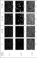
도 2 는 실시예들에서 냉각-가열 사이클 전후의 접착층의 단면 표면의 SEM 이미지들이다.
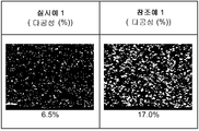
도 3 은 실시예들에서 접착층의 단면 표면의 SEM 이미지들이다.
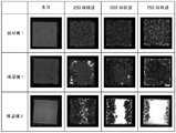
도 4 는 실시예들에서 냉각-가열 사이클 전후의 접착된 부분의 SAT 이미지들이다.
| 실시예 1 | 비교예 1 | 비교예 2 | 참조예 1 | |
| 접착 재료 | ||||
| 은 필러 | 필러 1 (89.9 wt%) |
필러 1 (94.9 wt%) |
필러 2 (90.24 wt%) |
필러 1 (89.9 wt%) |
| 수지 | 수지 1 (5.0 wt%) |
- |
- |
수지 1 (5.0 wt%) |
| 첨가제 | DBU (0.2 wt%) |
DBU (0.2 wt%) |
페르부틸 D (0.2 wt%) |
DBU (0.2 wt%) |
| 용매 | BC (4.9 wt%) |
BC (4.9 wt%) |
BCA/DPG 1/1 (9.56 wt%) |
BC (4.9 wt%) |
| 열 전도성 (W/mK) |
175 | 270 | 200 | 115 |
| 응력 감소 시험 (휨의 측정 (㎛)) |
||||
| 칩 | 139 | 170 | 160 | 149 |
| 기판 | 330 | 470 | 410 | 375 |
| 신뢰성 시험 (냉각-가열 사이클 전후의 다공성의 측정 (%)) |
||||
| 초기 | 6.5 | 1.0 | 13.0 | 17.0 |
| 250 사이클 | 7.0 | 1.5 | 15.0 | 미결정 |
| 500 사이클 | 11.0 | 3.0 | 23.0 | |
| 750 사이클 | 13.5 | 8.5 | 19.5 |
Claims (11)
- 은 필러 (filler) 및 수지 입자들을 포함하는 소결가능한 접착 재료로서,
상기 은 필러는 10 nm 이하의 산술 평균 조도 (Ra) 를 갖는 플레이크 (flake) 형상 필러를 포함하고;
상기 수지 입자들은 10 GPa 이하의 탄성률 (E), 및 200 ℃ 이상의 열 분해 온도를 갖는, 소결가능한 접착 재료. - 제 1 항에 있어서,
상기 은 필러의 함유량은 상기 접착 재료의 고체 성분들의 총 질량의 90 질량% 이상 및 99.9 질량% 이하인, 소결가능한 접착 재료. - 제 1 항 또는 제 2 항에 있어서,
상기 수지 입자들의 탄성률 (E) 은 100 MPa 이하인, 소결가능한 접착 재료. - 제 1 항 내지 제 3 항 중 어느 한 항에 있어서,
상기 수지 입자들은 실리콘 고무 입자들 및/또는 플루오로고무 입자들을 포함하는, 소결가능한 접착 재료. - 제 1 항 내지 제 4 항 중 어느 한 항에 있어서,
상기 은 필러는 결정질 플레이크 형상 필러를 포함하는, 소결가능한 접착 재료. - 제 1 항 내지 제 5 항 중 어느 한 항에 있어서,
첨가제를 더 포함하는, 소결가능한 접착 재료. - 제 1 항 내지 제 6 항 중 어느 한 항에 있어서,
용매를 더 포함하는, 소결가능한 접착 재료. - 분산된 수지 입자들을 포함하는 은 소결 제품으로서,
상기 수지 입자들은 10 GPa 이하의 탄성률 (E), 및 200 ℃ 이상의 열 분해 온도를 갖는, 은 소결 제품. - 제 8 항에 있어서,
10% 이하의 평균 다공성을 갖는, 은 소결 제품. - 제 8 항 또는 제 9 항에 기재된 은 소결 제품에 의해 접착된 접착된 물품.
- 반도체 디바이스를 제조하는 방법으로서,
접착될 2 개의 부재들을 제공하는 단계;
상기 2 개의 부재들의 접착될 표면들이 그 사이에 접착 재료를 두고 서로 마주하도록 상기 2 개의 부재들 및 접착 재료를 배치하는 단계; 및
상기 2 개의 부재들을 그 사이에 상기 접착 재료를 두고 미리 결정된 온도까지 가열하는 단계를 포함하고,
상기 접착 재료는 은 필러 (filler) 및 수지 입자들을 포함하는 소결가능한 접착 재료이고,
상기 은 필러는 10 nm 이하의 산술 평균 조도 (Ra) 를 갖는 플레이크 (flake) 형상 필러를 포함하고;
상기 수지 입자들은 10 GPa 이하의 탄성률 (E), 및 200 ℃ 이상의 열 분해 온도를 갖는, 반도체 디바이스를 제조하는 방법.
Applications Claiming Priority (1)
| Application Number | Priority Date | Filing Date | Title |
|---|---|---|---|
| PCT/JP2014/084765 WO2016103528A1 (en) | 2014-12-26 | 2014-12-26 | Sinterable bonding material and semiconductor device using the same |
Publications (2)
| Publication Number | Publication Date |
|---|---|
| KR20170101276A true KR20170101276A (ko) | 2017-09-05 |
| KR102226649B1 KR102226649B1 (ko) | 2021-03-10 |
Family
ID=56149608
Family Applications (1)
| Application Number | Title | Priority Date | Filing Date |
|---|---|---|---|
| KR1020177020657A Active KR102226649B1 (ko) | 2014-12-26 | 2014-12-26 | 소결가능한 접착 재료 및 그것을 사용한 반도체 디바이스 |
Country Status (7)
| Country | Link |
|---|---|
| US (1) | US10446518B2 (ko) |
| EP (1) | EP3238239A4 (ko) |
| JP (1) | JP6571196B2 (ko) |
| KR (1) | KR102226649B1 (ko) |
| CN (1) | CN107735854B (ko) |
| TW (1) | TWI679709B (ko) |
| WO (1) | WO2016103528A1 (ko) |
Families Citing this family (14)
| Publication number | Priority date | Publication date | Assignee | Title |
|---|---|---|---|---|
| JP6729143B2 (ja) * | 2015-10-29 | 2020-07-22 | 三菱マテリアル株式会社 | 樹脂組成物、接合体及び半導体装置 |
| JP6888401B2 (ja) | 2017-04-28 | 2021-06-16 | 日亜化学工業株式会社 | 金属粉焼結ペースト及びその製造方法、ならびに導電性材料の製造方法 |
| JP6890520B2 (ja) * | 2017-10-04 | 2021-06-18 | 三菱電機株式会社 | 電力用半導体装置 |
| SG11202103798VA (en) * | 2018-10-26 | 2021-05-28 | Mitsui Chemicals Inc | Method of manufacturing substrate layered body and layered body |
| WO2020241739A1 (ja) * | 2019-05-29 | 2020-12-03 | 国立大学法人大阪大学 | 接合構造体の製造方法、及び接合構造体 |
| JP7539988B2 (ja) * | 2019-12-20 | 2024-08-26 | ヘンケル・アクチェンゲゼルシャフト・ウント・コムパニー・コマンディットゲゼルシャフト・アウフ・アクチェン | 金属結合用の銅合金を含有する銀焼結組成物 |
| JP7502598B2 (ja) * | 2020-01-29 | 2024-06-19 | 日亜化学工業株式会社 | 半導体装置と半導体装置の製造方法 |
| JP7562372B2 (ja) * | 2020-10-30 | 2024-10-07 | トクセン工業株式会社 | カーボンナノチューブ複合線 |
| US12539566B2 (en) * | 2020-12-16 | 2026-02-03 | Heraeus Deutschland GmbH & Co. KG | Sintering paste and use thereof for connecting components |
| JP7205705B2 (ja) * | 2021-03-05 | 2023-01-17 | 株式会社リコー | 造形液及び造形物の製造方法 |
| US11938543B2 (en) * | 2021-04-09 | 2024-03-26 | Heraeus Deutschland GmbH & Co. KG | Silver sintering preparation and the use thereof for the connecting of electronic components |
| TWI848848B (zh) * | 2023-11-08 | 2024-07-11 | 同欣電子工業股份有限公司 | 減少基板於構裝製程發生翹曲的方法 |
| TWI887998B (zh) * | 2024-02-02 | 2025-06-21 | 先豐通訊股份有限公司 | 電路板及其製造方法 |
| JP2026004028A (ja) * | 2024-06-25 | 2026-01-14 | 日東電工株式会社 | 焼結接合用シート、及び、焼結接合用シートの製造方法 |
Citations (2)
| Publication number | Priority date | Publication date | Assignee | Title |
|---|---|---|---|---|
| KR20120022846A (ko) * | 2009-07-21 | 2012-03-12 | 니치아 카가쿠 고교 가부시키가이샤 | 도전성 재료의 제조 방법, 그 방법에 의해 얻어진 도전성 재료, 그 도전성 재료를 포함하는 전자 기기 및 발광 장치 |
| JP2014196527A (ja) * | 2013-03-29 | 2014-10-16 | トクセン工業株式会社 | フレーク状の微小粒子 |
Family Cites Families (31)
| Publication number | Priority date | Publication date | Assignee | Title |
|---|---|---|---|---|
| JPS60120778A (ja) * | 1983-12-05 | 1985-06-28 | Hitachi Chem Co Ltd | 導電性接着剤組成物 |
| US5232962A (en) * | 1991-10-09 | 1993-08-03 | Quantum Materials, Inc. | Adhesive bonding composition with bond line limiting spacer system |
| JP2983816B2 (ja) * | 1993-10-29 | 1999-11-29 | 住友ベークライト株式会社 | 導電性樹脂ペースト |
| JP3760578B2 (ja) * | 1997-07-07 | 2006-03-29 | ソニー株式会社 | 銀ペーストダイボンド材および半導体装置 |
| JPH1144705A (ja) * | 1997-07-28 | 1999-02-16 | Denso Corp | 半導体加速度センサおよびその製造方法 |
| JP2001170957A (ja) * | 1999-12-20 | 2001-06-26 | Tokuyama Corp | ポリプロピレン射出成形体 |
| JP2002367427A (ja) * | 2001-06-12 | 2002-12-20 | Murata Mfg Co Ltd | 導電性ぺースト、電子部品 |
| JP2005220486A (ja) * | 2004-02-06 | 2005-08-18 | Toray Ind Inc | フッ素繊維交織織物および複合材料 |
| JP4487143B2 (ja) | 2004-12-27 | 2010-06-23 | ナミックス株式会社 | 銀微粒子及びその製造方法並びに導電ペースト及びその製造方法 |
| JP4770533B2 (ja) | 2005-05-16 | 2011-09-14 | 富士電機株式会社 | 半導体装置の製造方法および半導体装置 |
| WO2008062548A1 (fr) | 2006-11-24 | 2008-05-29 | Nihon Handa Co., Ltd. | Composition de particules métalliques pâteuses et procédé de réunion |
| JP4470193B2 (ja) | 2008-05-01 | 2010-06-02 | ニホンハンダ株式会社 | 加熱焼結性銀粒子の製造方法、固形状銀の製造方法、金属製部材の接合方法、プリント配線板の製造方法および電気回路接続用バンプの製造方法 |
| JP5011225B2 (ja) | 2008-07-09 | 2012-08-29 | ニホンハンダ株式会社 | 金属製部材用接合剤、金属製部材接合体の製造方法、金属製部材接合体、および電気回路接続用バンプの製造方法 |
| JP5311337B2 (ja) * | 2008-11-28 | 2013-10-09 | セイコーインスツル株式会社 | サーマルヘッド、サーマルプリンタ及びサーマルヘッドの製造方法 |
| JP2010171271A (ja) | 2009-01-23 | 2010-08-05 | Renesas Technology Corp | 半導体装置およびその製造方法 |
| JP2010180327A (ja) * | 2009-02-05 | 2010-08-19 | Nippon Steel Chem Co Ltd | ポリマー組成物 |
| EP2227056B1 (en) | 2009-03-02 | 2019-04-24 | Alcatel Lucent | Method for enhancing the handover of a mobile station and base station for carrying out the method |
| JP4633857B1 (ja) | 2009-04-16 | 2011-02-16 | ニホンハンダ株式会社 | 有機物被覆金属粒子の加熱焼結性の評価方法、加熱焼結性金属ペーストの製造方法、および金属製部材接合体の製造方法 |
| JP5611537B2 (ja) * | 2009-04-28 | 2014-10-22 | 日立化成株式会社 | 導電性接合材料、それを用いた接合方法、並びにそれによって接合された半導体装置 |
| JP2011040915A (ja) | 2009-08-08 | 2011-02-24 | Minoru Tomizawa | 携帯通信端末機電源・モード切り替えシステム |
| JP5426413B2 (ja) | 2010-01-28 | 2014-02-26 | ハリマ化成株式会社 | 銀ナノ粒子の製造方法 |
| JP4928639B2 (ja) | 2010-03-15 | 2012-05-09 | Dowaエレクトロニクス株式会社 | 接合材およびそれを用いた接合方法 |
| JP2011198674A (ja) | 2010-03-23 | 2011-10-06 | Mitsubishi Electric Corp | 導電性接合材料、これを用いた半導体装置および半導体装置の製造方法 |
| JP4870223B1 (ja) * | 2010-09-02 | 2012-02-08 | ニホンハンダ株式会社 | ペースト状銀粒子組成物、金属製部材接合体の製造方法および金属製部材接合体 |
| JP2012085582A (ja) | 2010-10-20 | 2012-05-10 | Kanagawa Acad Of Sci & Technol | フルオロキノロン系薬剤耐性菌の検出方法及びそのためのプライマー |
| WO2012070262A1 (ja) * | 2010-11-22 | 2012-05-31 | Dowaエレクトロニクス株式会社 | 接合材料および接合体、並びに接合方法 |
| JP2013041884A (ja) * | 2011-08-11 | 2013-02-28 | Furukawa Electric Co Ltd:The | 半導体装置 |
| JP5425962B2 (ja) | 2012-04-04 | 2014-02-26 | ニホンハンダ株式会社 | 加熱焼結性銀粒子の製造方法、ペースト状銀粒子組成物、固形状銀の製造方法、金属製部材の接合方法、プリント配線板の製造方法および電気回路接続用バンプの製造方法 |
| JP2014029897A (ja) | 2012-07-31 | 2014-02-13 | Hitachi Ltd | 導電性接合体およびそれを用いた半導体装置 |
| JP5567636B2 (ja) * | 2012-10-05 | 2014-08-06 | 京セラケミカル株式会社 | 半導体接着用熱硬化型樹脂組成物及び半導体装置 |
| US20150262728A1 (en) * | 2014-03-11 | 2015-09-17 | E I Du Pont De Nemours And Company | Electrically conductive paste composition and method of forming an electrical circuit on a polymer substrate |
-
2014
- 2014-12-26 JP JP2017534360A patent/JP6571196B2/ja active Active
- 2014-12-26 CN CN201480084354.7A patent/CN107735854B/zh active Active
- 2014-12-26 EP EP14909128.2A patent/EP3238239A4/en not_active Ceased
- 2014-12-26 KR KR1020177020657A patent/KR102226649B1/ko active Active
- 2014-12-26 WO PCT/JP2014/084765 patent/WO2016103528A1/en not_active Ceased
-
2015
- 2015-12-11 TW TW104141663A patent/TWI679709B/zh active
-
2017
- 2017-06-23 US US15/631,282 patent/US10446518B2/en active Active
Patent Citations (2)
| Publication number | Priority date | Publication date | Assignee | Title |
|---|---|---|---|---|
| KR20120022846A (ko) * | 2009-07-21 | 2012-03-12 | 니치아 카가쿠 고교 가부시키가이샤 | 도전성 재료의 제조 방법, 그 방법에 의해 얻어진 도전성 재료, 그 도전성 재료를 포함하는 전자 기기 및 발광 장치 |
| JP2014196527A (ja) * | 2013-03-29 | 2014-10-16 | トクセン工業株式会社 | フレーク状の微小粒子 |
Also Published As
| Publication number | Publication date |
|---|---|
| JP2018502455A (ja) | 2018-01-25 |
| US10446518B2 (en) | 2019-10-15 |
| CN107735854A (zh) | 2018-02-23 |
| KR102226649B1 (ko) | 2021-03-10 |
| US20170294404A1 (en) | 2017-10-12 |
| EP3238239A4 (en) | 2018-07-25 |
| WO2016103528A1 (en) | 2016-06-30 |
| JP6571196B2 (ja) | 2019-09-04 |
| TW201628103A (zh) | 2016-08-01 |
| EP3238239A1 (en) | 2017-11-01 |
| TWI679709B (zh) | 2019-12-11 |
| CN107735854B (zh) | 2020-12-15 |
Similar Documents
| Publication | Publication Date | Title |
|---|---|---|
| KR102226649B1 (ko) | 소결가능한 접착 재료 및 그것을 사용한 반도체 디바이스 | |
| JP5667190B2 (ja) | 酸化剤を含む金属ペースト | |
| EP3255112B1 (en) | Thermoconductive electroconductive adhesive composition | |
| TWI694884B (zh) | 可燒結黏著材料以及使用上述材料之半導體裝置及製造半導體裝置之方法 | |
| KR102345811B1 (ko) | 도전성 조성물 및 그것을 사용한 전자 부품 | |
| EP2940093B1 (en) | Thermally-conductive, electrically-conductive adhesive composition | |
| WO2019013231A1 (ja) | 導電性接着剤組成物 | |
| TW202035637A (zh) | 導電性接著劑組成物 | |
| TWI655693B (zh) | 半導體裝置之製造方法 | |
| JP2017031341A (ja) | 半導体接着用熱硬化型樹脂組成物及びそれを用いた半導体装置 | |
| JP2024070935A (ja) | 保持装置、および保持装置の製造方法 | |
| WO2023127968A1 (ja) | 接合用シート、接合用シートの製造方法、及び接合体の製造方法 | |
| JP2023098497A (ja) | 接合体の製造方法 | |
| WO2023127969A1 (ja) | 接合用シート、及び接合体の製造方法 | |
| WO2016056655A1 (ja) | 半導体デバイスの製造法 | |
| JP2023098496A (ja) | 接合用シート、及び接合体の製造方法 |
Legal Events
| Date | Code | Title | Description |
|---|---|---|---|
| PA0105 | International application |
St.27 status event code: A-0-1-A10-A15-nap-PA0105 |
|
| PG1501 | Laying open of application |
St.27 status event code: A-1-1-Q10-Q12-nap-PG1501 |
|
| A201 | Request for examination | ||
| P11-X000 | Amendment of application requested |
St.27 status event code: A-2-2-P10-P11-nap-X000 |
|
| P13-X000 | Application amended |
St.27 status event code: A-2-2-P10-P13-nap-X000 |
|
| PA0201 | Request for examination |
St.27 status event code: A-1-2-D10-D11-exm-PA0201 |
|
| D13-X000 | Search requested |
St.27 status event code: A-1-2-D10-D13-srh-X000 |
|
| D14-X000 | Search report completed |
St.27 status event code: A-1-2-D10-D14-srh-X000 |
|
| P22-X000 | Classification modified |
St.27 status event code: A-2-2-P10-P22-nap-X000 |
|
| E902 | Notification of reason for refusal | ||
| PE0902 | Notice of grounds for rejection |
St.27 status event code: A-1-2-D10-D21-exm-PE0902 |
|
| E13-X000 | Pre-grant limitation requested |
St.27 status event code: A-2-3-E10-E13-lim-X000 |
|
| P11-X000 | Amendment of application requested |
St.27 status event code: A-2-2-P10-P11-nap-X000 |
|
| P13-X000 | Application amended |
St.27 status event code: A-2-2-P10-P13-nap-X000 |
|
| E701 | Decision to grant or registration of patent right | ||
| PE0701 | Decision of registration |
St.27 status event code: A-1-2-D10-D22-exm-PE0701 |
|
| GRNT | Written decision to grant | ||
| PR0701 | Registration of establishment |
St.27 status event code: A-2-4-F10-F11-exm-PR0701 |
|
| PR1002 | Payment of registration fee |
St.27 status event code: A-2-2-U10-U12-oth-PR1002 Fee payment year number: 1 |
|
| PG1601 | Publication of registration |
St.27 status event code: A-4-4-Q10-Q13-nap-PG1601 |
|
| PN2301 | Change of applicant |
St.27 status event code: A-5-5-R10-R11-asn-PN2301 |
|
| PN2301 | Change of applicant |
St.27 status event code: A-5-5-R10-R14-asn-PN2301 |
|
| PR1001 | Payment of annual fee |
St.27 status event code: A-4-4-U10-U11-oth-PR1001 Fee payment year number: 4 |
|
| P22-X000 | Classification modified |
St.27 status event code: A-4-4-P10-P22-nap-X000 |
|
| P22-X000 | Classification modified |
St.27 status event code: A-4-4-P10-P22-nap-X000 |