KR20170119801A - 유기 발광 표시 장치 및 유기 발광 표시 장치의 제조 방법 - Google Patents
유기 발광 표시 장치 및 유기 발광 표시 장치의 제조 방법 Download PDFInfo
- Publication number
- KR20170119801A KR20170119801A KR1020160047857A KR20160047857A KR20170119801A KR 20170119801 A KR20170119801 A KR 20170119801A KR 1020160047857 A KR1020160047857 A KR 1020160047857A KR 20160047857 A KR20160047857 A KR 20160047857A KR 20170119801 A KR20170119801 A KR 20170119801A
- Authority
- KR
- South Korea
- Prior art keywords
- layer
- insulating layer
- disposed
- substrate
- electrode
- Prior art date
- Legal status (The legal status is an assumption and is not a legal conclusion. Google has not performed a legal analysis and makes no representation as to the accuracy of the status listed.)
- Ceased
Links
Images







Classifications
-
- H01L27/3262—
-
- H—ELECTRICITY
- H10—SEMICONDUCTOR DEVICES; ELECTRIC SOLID-STATE DEVICES NOT OTHERWISE PROVIDED FOR
- H10K—ORGANIC ELECTRIC SOLID-STATE DEVICES
- H10K59/00—Integrated devices, or assemblies of multiple devices, comprising at least one organic light-emitting element covered by group H10K50/00
- H10K59/10—OLED displays
- H10K59/12—Active-matrix OLED [AMOLED] displays
- H10K59/121—Active-matrix OLED [AMOLED] displays characterised by the geometry or disposition of pixel elements
- H10K59/1213—Active-matrix OLED [AMOLED] displays characterised by the geometry or disposition of pixel elements the pixel elements being TFTs
-
- H01L21/02065—
-
- H01L21/823462—
-
- H01L27/3218—
-
- H01L27/3246—
-
- H01L27/3258—
-
- H01L29/78618—
-
- H01L29/7869—
-
- H—ELECTRICITY
- H10—SEMICONDUCTOR DEVICES; ELECTRIC SOLID-STATE DEVICES NOT OTHERWISE PROVIDED FOR
- H10D—INORGANIC ELECTRIC SEMICONDUCTOR DEVICES
- H10D30/00—Field-effect transistors [FET]
- H10D30/60—Insulated-gate field-effect transistors [IGFET]
- H10D30/67—Thin-film transistors [TFT]
- H10D30/6704—Thin-film transistors [TFT] having supplementary regions or layers in the thin films or in the insulated bulk substrates for controlling properties of the device
- H10D30/6713—Thin-film transistors [TFT] having supplementary regions or layers in the thin films or in the insulated bulk substrates for controlling properties of the device characterised by the properties of the source or drain regions, e.g. compositions or sectional shapes
-
- H—ELECTRICITY
- H10—SEMICONDUCTOR DEVICES; ELECTRIC SOLID-STATE DEVICES NOT OTHERWISE PROVIDED FOR
- H10D—INORGANIC ELECTRIC SEMICONDUCTOR DEVICES
- H10D30/00—Field-effect transistors [FET]
- H10D30/60—Insulated-gate field-effect transistors [IGFET]
- H10D30/67—Thin-film transistors [TFT]
- H10D30/674—Thin-film transistors [TFT] characterised by the active materials
- H10D30/6755—Oxide semiconductors, e.g. zinc oxide, copper aluminium oxide or cadmium stannate
-
- H—ELECTRICITY
- H10—SEMICONDUCTOR DEVICES; ELECTRIC SOLID-STATE DEVICES NOT OTHERWISE PROVIDED FOR
- H10D—INORGANIC ELECTRIC SEMICONDUCTOR DEVICES
- H10D64/00—Electrodes of devices having potential barriers
- H10D64/01—Manufacture or treatment
- H10D64/031—Manufacture or treatment of data-storage electrodes
- H10D64/033—Manufacture or treatment of data-storage electrodes comprising ferroelectric layers
-
- H—ELECTRICITY
- H10—SEMICONDUCTOR DEVICES; ELECTRIC SOLID-STATE DEVICES NOT OTHERWISE PROVIDED FOR
- H10D—INORGANIC ELECTRIC SEMICONDUCTOR DEVICES
- H10D84/00—Integrated devices formed in or on semiconductor substrates that comprise only semiconducting layers, e.g. on Si wafers or on GaAs-on-Si wafers
- H10D84/01—Manufacture or treatment
- H10D84/0123—Integrating together multiple components covered by H10D12/00 or H10D30/00, e.g. integrating multiple IGBTs
- H10D84/0126—Integrating together multiple components covered by H10D12/00 or H10D30/00, e.g. integrating multiple IGBTs the components including insulated gates, e.g. IGFETs
- H10D84/0144—Manufacturing their gate insulating layers
-
- H—ELECTRICITY
- H10—SEMICONDUCTOR DEVICES; ELECTRIC SOLID-STATE DEVICES NOT OTHERWISE PROVIDED FOR
- H10D—INORGANIC ELECTRIC SEMICONDUCTOR DEVICES
- H10D86/00—Integrated devices formed in or on insulating or conducting substrates, e.g. formed in silicon-on-insulator [SOI] substrates or on stainless steel or glass substrates
- H10D86/40—Integrated devices formed in or on insulating or conducting substrates, e.g. formed in silicon-on-insulator [SOI] substrates or on stainless steel or glass substrates characterised by multiple TFTs
- H10D86/421—Integrated devices formed in or on insulating or conducting substrates, e.g. formed in silicon-on-insulator [SOI] substrates or on stainless steel or glass substrates characterised by multiple TFTs having a particular composition, shape or crystalline structure of the active layer
- H10D86/423—Integrated devices formed in or on insulating or conducting substrates, e.g. formed in silicon-on-insulator [SOI] substrates or on stainless steel or glass substrates characterised by multiple TFTs having a particular composition, shape or crystalline structure of the active layer comprising semiconductor materials not belonging to the Group IV, e.g. InGaZnO
-
- H—ELECTRICITY
- H10—SEMICONDUCTOR DEVICES; ELECTRIC SOLID-STATE DEVICES NOT OTHERWISE PROVIDED FOR
- H10D—INORGANIC ELECTRIC SEMICONDUCTOR DEVICES
- H10D86/00—Integrated devices formed in or on insulating or conducting substrates, e.g. formed in silicon-on-insulator [SOI] substrates or on stainless steel or glass substrates
- H10D86/40—Integrated devices formed in or on insulating or conducting substrates, e.g. formed in silicon-on-insulator [SOI] substrates or on stainless steel or glass substrates characterised by multiple TFTs
- H10D86/451—Integrated devices formed in or on insulating or conducting substrates, e.g. formed in silicon-on-insulator [SOI] substrates or on stainless steel or glass substrates characterised by multiple TFTs characterised by the compositions or shapes of the interlayer dielectrics
-
- H—ELECTRICITY
- H10—SEMICONDUCTOR DEVICES; ELECTRIC SOLID-STATE DEVICES NOT OTHERWISE PROVIDED FOR
- H10D—INORGANIC ELECTRIC SEMICONDUCTOR DEVICES
- H10D86/00—Integrated devices formed in or on insulating or conducting substrates, e.g. formed in silicon-on-insulator [SOI] substrates or on stainless steel or glass substrates
- H10D86/40—Integrated devices formed in or on insulating or conducting substrates, e.g. formed in silicon-on-insulator [SOI] substrates or on stainless steel or glass substrates characterised by multiple TFTs
- H10D86/481—Integrated devices formed in or on insulating or conducting substrates, e.g. formed in silicon-on-insulator [SOI] substrates or on stainless steel or glass substrates characterised by multiple TFTs integrated with passive devices, e.g. auxiliary capacitors
-
- H—ELECTRICITY
- H10—SEMICONDUCTOR DEVICES; ELECTRIC SOLID-STATE DEVICES NOT OTHERWISE PROVIDED FOR
- H10D—INORGANIC ELECTRIC SEMICONDUCTOR DEVICES
- H10D86/00—Integrated devices formed in or on insulating or conducting substrates, e.g. formed in silicon-on-insulator [SOI] substrates or on stainless steel or glass substrates
- H10D86/40—Integrated devices formed in or on insulating or conducting substrates, e.g. formed in silicon-on-insulator [SOI] substrates or on stainless steel or glass substrates characterised by multiple TFTs
- H10D86/60—Integrated devices formed in or on insulating or conducting substrates, e.g. formed in silicon-on-insulator [SOI] substrates or on stainless steel or glass substrates characterised by multiple TFTs wherein the TFTs are in active matrices
-
- H—ELECTRICITY
- H10—SEMICONDUCTOR DEVICES; ELECTRIC SOLID-STATE DEVICES NOT OTHERWISE PROVIDED FOR
- H10K—ORGANIC ELECTRIC SOLID-STATE DEVICES
- H10K59/00—Integrated devices, or assemblies of multiple devices, comprising at least one organic light-emitting element covered by group H10K50/00
- H10K59/10—OLED displays
- H10K59/12—Active-matrix OLED [AMOLED] displays
-
- H—ELECTRICITY
- H10—SEMICONDUCTOR DEVICES; ELECTRIC SOLID-STATE DEVICES NOT OTHERWISE PROVIDED FOR
- H10K—ORGANIC ELECTRIC SOLID-STATE DEVICES
- H10K59/00—Integrated devices, or assemblies of multiple devices, comprising at least one organic light-emitting element covered by group H10K50/00
- H10K59/10—OLED displays
- H10K59/12—Active-matrix OLED [AMOLED] displays
- H10K59/1201—Manufacture or treatment
-
- H—ELECTRICITY
- H10—SEMICONDUCTOR DEVICES; ELECTRIC SOLID-STATE DEVICES NOT OTHERWISE PROVIDED FOR
- H10K—ORGANIC ELECTRIC SOLID-STATE DEVICES
- H10K59/00—Integrated devices, or assemblies of multiple devices, comprising at least one organic light-emitting element covered by group H10K50/00
- H10K59/10—OLED displays
- H10K59/12—Active-matrix OLED [AMOLED] displays
- H10K59/121—Active-matrix OLED [AMOLED] displays characterised by the geometry or disposition of pixel elements
-
- H—ELECTRICITY
- H10—SEMICONDUCTOR DEVICES; ELECTRIC SOLID-STATE DEVICES NOT OTHERWISE PROVIDED FOR
- H10K—ORGANIC ELECTRIC SOLID-STATE DEVICES
- H10K59/00—Integrated devices, or assemblies of multiple devices, comprising at least one organic light-emitting element covered by group H10K50/00
- H10K59/10—OLED displays
- H10K59/12—Active-matrix OLED [AMOLED] displays
- H10K59/121—Active-matrix OLED [AMOLED] displays characterised by the geometry or disposition of pixel elements
- H10K59/1216—Active-matrix OLED [AMOLED] displays characterised by the geometry or disposition of pixel elements the pixel elements being capacitors
-
- H—ELECTRICITY
- H10—SEMICONDUCTOR DEVICES; ELECTRIC SOLID-STATE DEVICES NOT OTHERWISE PROVIDED FOR
- H10K—ORGANIC ELECTRIC SOLID-STATE DEVICES
- H10K59/00—Integrated devices, or assemblies of multiple devices, comprising at least one organic light-emitting element covered by group H10K50/00
- H10K59/10—OLED displays
- H10K59/12—Active-matrix OLED [AMOLED] displays
- H10K59/122—Pixel-defining structures or layers, e.g. banks
-
- H—ELECTRICITY
- H10—SEMICONDUCTOR DEVICES; ELECTRIC SOLID-STATE DEVICES NOT OTHERWISE PROVIDED FOR
- H10K—ORGANIC ELECTRIC SOLID-STATE DEVICES
- H10K59/00—Integrated devices, or assemblies of multiple devices, comprising at least one organic light-emitting element covered by group H10K50/00
- H10K59/10—OLED displays
- H10K59/12—Active-matrix OLED [AMOLED] displays
- H10K59/123—Connection of the pixel electrodes to the thin film transistors [TFT]
-
- H—ELECTRICITY
- H10—SEMICONDUCTOR DEVICES; ELECTRIC SOLID-STATE DEVICES NOT OTHERWISE PROVIDED FOR
- H10K—ORGANIC ELECTRIC SOLID-STATE DEVICES
- H10K59/00—Integrated devices, or assemblies of multiple devices, comprising at least one organic light-emitting element covered by group H10K50/00
- H10K59/10—OLED displays
- H10K59/12—Active-matrix OLED [AMOLED] displays
- H10K59/124—Insulating layers formed between TFT elements and OLED elements
-
- H—ELECTRICITY
- H10—SEMICONDUCTOR DEVICES; ELECTRIC SOLID-STATE DEVICES NOT OTHERWISE PROVIDED FOR
- H10K—ORGANIC ELECTRIC SOLID-STATE DEVICES
- H10K59/00—Integrated devices, or assemblies of multiple devices, comprising at least one organic light-emitting element covered by group H10K50/00
- H10K59/30—Devices specially adapted for multicolour light emission
- H10K59/35—Devices specially adapted for multicolour light emission comprising red-green-blue [RGB] subpixels
- H10K59/353—Devices specially adapted for multicolour light emission comprising red-green-blue [RGB] subpixels characterised by the geometrical arrangement of the RGB subpixels
-
- H—ELECTRICITY
- H10—SEMICONDUCTOR DEVICES; ELECTRIC SOLID-STATE DEVICES NOT OTHERWISE PROVIDED FOR
- H10K—ORGANIC ELECTRIC SOLID-STATE DEVICES
- H10K71/00—Manufacture or treatment specially adapted for the organic devices covered by this subclass
-
- H—ELECTRICITY
- H10—SEMICONDUCTOR DEVICES; ELECTRIC SOLID-STATE DEVICES NOT OTHERWISE PROVIDED FOR
- H10P—GENERIC PROCESSES OR APPARATUS FOR THE MANUFACTURE OR TREATMENT OF DEVICES COVERED BY CLASS H10
- H10P14/00—Formation of materials, e.g. in the shape of layers or pillars
- H10P14/60—Formation of materials, e.g. in the shape of layers or pillars of insulating materials
-
- H—ELECTRICITY
- H10—SEMICONDUCTOR DEVICES; ELECTRIC SOLID-STATE DEVICES NOT OTHERWISE PROVIDED FOR
- H10P—GENERIC PROCESSES OR APPARATUS FOR THE MANUFACTURE OR TREATMENT OF DEVICES COVERED BY CLASS H10
- H10P70/00—Cleaning of wafers, substrates or parts of devices
- H10P70/20—Cleaning during device manufacture
- H10P70/23—Cleaning during device manufacture during, before or after processing of insulating materials
- H10P70/237—Cleaning during device manufacture during, before or after processing of insulating materials the processing being a planarisation of insulating layers
-
- H—ELECTRICITY
- H10—SEMICONDUCTOR DEVICES; ELECTRIC SOLID-STATE DEVICES NOT OTHERWISE PROVIDED FOR
- H10P—GENERIC PROCESSES OR APPARATUS FOR THE MANUFACTURE OR TREATMENT OF DEVICES COVERED BY CLASS H10
- H10P95/00—Generic processes or apparatus for manufacture or treatments not covered by the other groups of this subclass
- H10P95/90—Thermal treatments, e.g. annealing or sintering
-
- H01L2227/323—
-
- H01L2251/303—
-
- H—ELECTRICITY
- H10—SEMICONDUCTOR DEVICES; ELECTRIC SOLID-STATE DEVICES NOT OTHERWISE PROVIDED FOR
- H10D—INORGANIC ELECTRIC SEMICONDUCTOR DEVICES
- H10D86/00—Integrated devices formed in or on insulating or conducting substrates, e.g. formed in silicon-on-insulator [SOI] substrates or on stainless steel or glass substrates
- H10D86/01—Manufacture or treatment
- H10D86/021—Manufacture or treatment of multiple TFTs
-
- H—ELECTRICITY
- H10—SEMICONDUCTOR DEVICES; ELECTRIC SOLID-STATE DEVICES NOT OTHERWISE PROVIDED FOR
- H10K—ORGANIC ELECTRIC SOLID-STATE DEVICES
- H10K2102/00—Constructional details relating to the organic devices covered by this subclass
Landscapes
- Engineering & Computer Science (AREA)
- Microelectronics & Electronic Packaging (AREA)
- Physics & Mathematics (AREA)
- Geometry (AREA)
- Manufacturing & Machinery (AREA)
- Electroluminescent Light Sources (AREA)
- Thin Film Transistor (AREA)
Abstract
Description
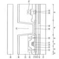
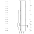
도 2는 도 1의 유기 발광 표시 장치에 포함된 컬러 필터를 설명하기 위한 단면도이다.
도 3 내지 도 11은 본 발명의 예시적인 실시예들에 따른 유기 발광 표시 장치의 제조 방법을 나타내는 단면도들이다.
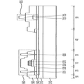
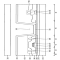
도 12는 본 발명의 예시적인 실시예들에 따른 유기 발광 표시 장치를 나타내는 단면도이다.
도 13은 본 발명의 예시적인 실시예들에 따른 유기 발광 표시 장치를 나타내는 단면도이다.
30: 드레인 영역 40: 하부 전극 영역
100: 유기 발광 표시 장치 110, 510: 기판
115, 515: 버퍼층 130, 530: 액티브층
140, 540: 보호 절연층 155: 보조 게이트 전극
170, 570: 게이트 전극 190, 590: 층간 절연층
210, 610: 소스 전극 230, 630: 드레인 전극
250, 650: 반도체 소자 255, 655: 스토리지 커패시터
270, 670: 평탄화층 275, 675: 개구
320, 720: 제1 전극 322: 보조 제1 전극
325, 725: 제2 전극 330, 730: 발광층
340, 740: 상부 전극 350, 750: 봉지 기판
405: 컬러 필터 410: 광차단 부재
541: 금속층 542: 제1 층
543: 제2 층 544: 예비 보호 절연층
545: 포토레지스트
Claims (20)
- 기판;
상기 기판 상에 배치되는 버퍼층;
상기 버퍼층 상에 배치되고, 소스 영역, 드레인 영역 및 채널 영역을 포함하는 액티브층;
상기 액티브층 상의 채널 영역에 배치되는 게이트 절연층;
상기 버퍼층, 상기 액티브층의 소스 및 드레인 영역들 및 상기 게이트 절연층 상에 배치되는 보호 절연층;
상기 보호 절연층 상의 상기 채널 영역에 배치되는 게이트 전극;
상기 게이트 전극 상에 배치되는 층간 절연층;
상기 층간 절연층 상에 배치되고, 상기 액티브층의 소스 및 드레인 영역들에 각기 접속되는 소스 및 드레인 전극들; 및
상기 기판 상에 배치되는 서브 화소 구조물을 포함하는 유기 발광 표시 장치. - 제 1 항에 있어서, 상기 버퍼층 및 상기 게이트 절연층은 산소를 포함하는 무기 물질을 포함하는 것을 특징으로 하는 유기 발광 표시 장치.
- 제 1 항에 있어서, 상기 버퍼층 및 상기 게이트 절연층은 산소를 포함하는 무기 물질로 구성되는 것을 특징으로 하는 유기 발광 표시 장치.
- 제 1 항에 있어서, 상기 액티브층은 산화물 반도체를 포함하는 것을 특징으로 하는 유기 발광 표시 장치.
- 제 1 항에 있어서, 상기 보호 절연층 및 상기 게이트 전극은 동일한 금속 물질을 포함하는 것을 특징으로 하는 유기 발광 표시 장치.
- 제 1 항에 있어서,
상기 게이트 전극 상에 배치되는 보조 게이트 전극을 더 포함하고,
상기 보조 게이트 전극은 상기 게이트 전극과 상기 층간 절연층 사이에 위치하는 것을 특징으로 하는 유기 발광 표시 장치. - 제 1 항에 있어서, 상기 서브 화소 구조물은,
상기 기판 상에 배치되는 하부 전극;
상기 하부 전극 상에 배치되는 발광층; 및
상기 발광층 상에 배치되는 상부 전극을 포함하는 것을 특징으로 하는 유기 발광 표시 장치. - 제 7 항에 있어서, 상기 액티브층이 상기 채널 영역으로부터 상기 드레인 영역으로의 방향으로 연장되고, 상기 연장된 부분이 하부 전극 영역으로 정의되며, 상기 액티브층의 연장된 부분은 상기 하부 전극으로 기능하고, 상기 보호 절연층 및 상기 층간 절연층은 상기 액티브층의 하부 전극 영역을 노출시키는 것을 특징으로 하는 유기 발광 표시 장치.
- 제 8 항에 있어서,
상기 기판 상에 배치되는 평탄화층을 더 포함하고,
상기 평탄화층은 상기 층간 절연층, 상기 소스 및 드레인 전극들 및 상기 보호 절연층을 덮고, 상기 액티브층의 상기 하부 전극 영역의 일부를 노출시키는 개구를 가지며, 상기 발광층은 상기 평탄화층의 개구에 배치되는 것을 특징으로 하는 유기 발광 표시 장치. - 기판;
상기 기판 상에 배치되는 버퍼층;
상기 버퍼층 상에 배치되고, 소스 영역, 드레인 영역 및 채널 영역을 포함하는 액티브층;
상기 액티브층 상의 채널 영역에 배치되는 게이트 절연층;
상기 게이트 절연층 상에 배치되는 게이트 전극;
상기 버퍼층, 상기 액티브층의 소스 및 드레인 영역들 및 상기 게이트 전극 상에 배치되는 보호 절연층;
상기 보호 절연층 상에 배치되는 층간 절연층;
상기 층간 절연층 상에 배치되고, 상기 액티브층의 소스 및 드레인 영역들에 각기 접속되는 소스 및 드레인 전극들; 및
상기 기판 상에 배치되는 서브 화소 구조물을 포함하는 유기 발광 표시 장치. - 제 10 항에 있어서, 상기 버퍼층 및 상기 게이트 절연층은 산소를 포함하는 무기 물질을 포함하고, 상기 액티브층은 산화물 반도체를 포함하는 것을 특징으로 하는 유기 발광 표시 장치.
- 제 10 항에 있어서, 상기 보호 절연층 및 상기 게이트 전극은 동일한 금속 물질을 포함하는 것을 특징으로 하는 유기 발광 표시 장치.
- 기판을 제공하는 단계;
상기 기판 상에 배치되는 버퍼층을 형성하는 단계;
상기 버퍼층 상에 소스 영역, 드레인 영역 및 채널 영역을 포함하는 액티브층을 형성하는 단계;
상기 액티브층 상의 채널 영역에 게이트 절연층을 형성하는 단계;
상기 버퍼층, 상기 액티브층의 소스 및 드레인 영역들 및 상기 게이트 절연층 상에 금속층을 형성하는 단계;
상기 기판 상에 열처리 공정을 수행하여 상기 금속층에 보호 절연층을 형성하는 단계;
상기 금속층을 부분적으로 제거하여 상기 보호 절연층 및 게이트 전극을 형성하는 단계;
상기 게이트 절연층 상에 층간 절연층을 형성하는 단계;
상기 층간 절연층 상에 상기 액티브층의 소스 및 드레인 영역들에 각기 접속되는 소스 및 드레인 전극들을 형성하는 단계; 및
상기 소스 및 드레인 전극들 상에 화소 구조물을 형성하는 단계를 포함하는 유기 발광 표시 장치의 제조 방법. - 제 13 항에 있어서, 상기 액티브층은 산화물 반도체를 포함하는 것을 특징으로 하는 유기 발광 표시 장치의 제조 방법.
- 제 14 항에 있어서, 상기 버퍼층 및 상기 게이트 절연층은 산소를 포함하는 무기 물질을 포함하는 것을 특징으로 하는 유기 발광 표시 장치의 제조 방법의 제조 방법.
- 제 15 항에 있어서, 상기 기판 상에 열처리 공정을 수행하는 경우,
상기 금속층과 상기 버퍼층이 접촉하는 부분에서 상기 금속층은 상기 버퍼층으로부터 상기 산소를 제공받고, 상기 금속층과 상기 액티브층의 소스 및 드레인 영역들이 접촉하는 부분에서 상기 금속층은 상기 액티브층으로부터 산소를 제공받으며, 상기 금속층과 상기 게이트 절연층이 접촉하는 부분에서 상기 금속층은 상기 게이트 절연층으로부터 상기 산소를 제공받는 것을 특징으로 하는 유기 발광 표시 장치의 제조 방법. - 제 16 항에 있어서, 상기 산소를 제공받은 상기 금속층은 상기 금속층의 일부가 금속 절연층으로 변환되고, 상기 금속 절연층이 상기 보호 절연층으로 정의되는 것을 특징으로 하는 유기 발광 표시 장치의 제조 방법.
- 제 17 항에 있어서, 상기 산소를 제공한 액티브층의 소스 및 드레인 영역들은 금속화되는 것을 특징으로 하는 유기 발광 표시 장치의 제조 방법.
- 제 13 항에 있어서, 상기 금속층을 부분적으로 제거하여 상기 보호 절연층 및 게이트 전극을 형성하는 단계는,
상기 게이트 절연층 상에 위치한 상기 금속층 상에 포토레지스트를 배치하는 단계;
상기 금속층을 식각하는 단계; 및
상기 포토레지스트가 위치한 부분에 상기 게이트 전극 및 상기 버퍼층, 상기 액티브층의 소스 및 드레인 영역들 및 상기 게이트 절연층 상에 보호 절연층이 형성되는 단계를 포함하는 것을 특징으로 하는 유기 발광 표시 장치의 제조 방법. - 제 13 항에 있어서, 상기 보호 절연층 및 상기 게이트 전극은 동일한 금속 물질을 포함하는 것을 특징으로 하는 유기 발광 표시 장치의 제조 방법.
Priority Applications (5)
| Application Number | Priority Date | Filing Date | Title |
|---|---|---|---|
| KR1020160047857A KR20170119801A (ko) | 2016-04-19 | 2016-04-19 | 유기 발광 표시 장치 및 유기 발광 표시 장치의 제조 방법 |
| US15/453,513 US10930721B2 (en) | 2016-04-19 | 2017-03-08 | Organic light emitting display device and method of manufacturing organic light emitting display device |
| CN201710256835.7A CN107305907B (zh) | 2016-04-19 | 2017-04-19 | 有机发光显示装置和制造有机发光显示装置的方法 |
| US17/159,008 US11527594B2 (en) | 2016-04-19 | 2021-01-26 | Organic light emitting display device and method of manufacturing organic light emitting display device |
| KR1020240127088A KR20240144765A (ko) | 2016-04-19 | 2024-09-20 | 유기 발광 표시 장치 |
Applications Claiming Priority (1)
| Application Number | Priority Date | Filing Date | Title |
|---|---|---|---|
| KR1020160047857A KR20170119801A (ko) | 2016-04-19 | 2016-04-19 | 유기 발광 표시 장치 및 유기 발광 표시 장치의 제조 방법 |
Related Child Applications (1)
| Application Number | Title | Priority Date | Filing Date |
|---|---|---|---|
| KR1020240127088A Division KR20240144765A (ko) | 2016-04-19 | 2024-09-20 | 유기 발광 표시 장치 |
Publications (1)
| Publication Number | Publication Date |
|---|---|
| KR20170119801A true KR20170119801A (ko) | 2017-10-30 |
Family
ID=60039627
Family Applications (2)
| Application Number | Title | Priority Date | Filing Date |
|---|---|---|---|
| KR1020160047857A Ceased KR20170119801A (ko) | 2016-04-19 | 2016-04-19 | 유기 발광 표시 장치 및 유기 발광 표시 장치의 제조 방법 |
| KR1020240127088A Ceased KR20240144765A (ko) | 2016-04-19 | 2024-09-20 | 유기 발광 표시 장치 |
Family Applications After (1)
| Application Number | Title | Priority Date | Filing Date |
|---|---|---|---|
| KR1020240127088A Ceased KR20240144765A (ko) | 2016-04-19 | 2024-09-20 | 유기 발광 표시 장치 |
Country Status (3)
| Country | Link |
|---|---|
| US (2) | US10930721B2 (ko) |
| KR (2) | KR20170119801A (ko) |
| CN (1) | CN107305907B (ko) |
Families Citing this family (19)
| Publication number | Priority date | Publication date | Assignee | Title |
|---|---|---|---|---|
| KR102517726B1 (ko) * | 2017-12-05 | 2023-04-03 | 엘지디스플레이 주식회사 | 디지털 엑스레이 검출기용 어레이 기판과 이를 포함하는 디지털 엑스레이 검출기 및 그 제조 방법 |
| CN107885004B (zh) | 2017-12-06 | 2020-12-08 | 京东方科技集团股份有限公司 | 一种阵列基板、显示面板、显示装置及其制作工艺 |
| CN107968113B (zh) * | 2017-12-15 | 2021-01-08 | 京东方科技集团股份有限公司 | 阵列基板及其制备方法 |
| KR102763624B1 (ko) * | 2018-02-12 | 2025-02-10 | 삼성디스플레이 주식회사 | 유기 발광 표시 장치 |
| CN108598145B (zh) * | 2018-06-29 | 2021-08-31 | 上海天马微电子有限公司 | 一种有机发光显示面板和有机发光显示装置 |
| KR102075741B1 (ko) * | 2018-12-17 | 2020-02-10 | 엘지디스플레이 주식회사 | 표시패널 |
| CN110071069B (zh) * | 2019-04-19 | 2021-11-23 | 深圳市华星光电半导体显示技术有限公司 | 显示背板及其制作方法 |
| KR102814989B1 (ko) * | 2019-07-19 | 2025-05-30 | 삼성디스플레이 주식회사 | 표시 장치 |
| CN110391283B (zh) * | 2019-07-31 | 2022-05-27 | 上海天马微电子有限公司 | 有机发光显示面板和有机发光显示装置 |
| US11244994B2 (en) * | 2019-10-23 | 2022-02-08 | Wuhan China Star Optoelectronics Semiconductor Display Technology Co., Ltd. | Thin film transistor array substrate and organic light emitting diode panel |
| CN111106155B (zh) * | 2019-12-30 | 2022-10-25 | 武汉天马微电子有限公司 | 一种显示面板及显示装置 |
| KR20210128343A (ko) * | 2020-04-15 | 2021-10-26 | 에이에스엠 아이피 홀딩 비.브이. | 크롬 나이트라이드 층을 형성하는 방법 및 크롬 나이트라이드 층을 포함하는 구조 |
| KR102730649B1 (ko) * | 2020-04-20 | 2024-11-18 | 삼성디스플레이 주식회사 | 표시 장치 및 이의 제조 방법 |
| TWI750895B (zh) * | 2020-08-21 | 2021-12-21 | 友達光電股份有限公司 | 電子裝置 |
| CN112117321B (zh) * | 2020-10-21 | 2024-03-01 | 维信诺科技股份有限公司 | 显示面板及显示面板的制造方法 |
| CN112366223A (zh) * | 2020-11-23 | 2021-02-12 | Tcl华星光电技术有限公司 | Oled面板的制作方法、oled面板 |
| CN114335101B (zh) * | 2021-12-28 | 2024-11-22 | 深圳市华星光电半导体显示技术有限公司 | 显示面板及其制备方法 |
| KR102929195B1 (ko) * | 2021-12-30 | 2026-02-23 | 엘지디스플레이 주식회사 | 유기발광 표시장치 및 유기발광 표시패널 |
| CN114864636A (zh) | 2022-03-24 | 2022-08-05 | 深圳市华星光电半导体显示技术有限公司 | Oled显示面板及其制作方法 |
Family Cites Families (36)
| Publication number | Priority date | Publication date | Assignee | Title |
|---|---|---|---|---|
| KR100712295B1 (ko) * | 2005-06-22 | 2007-04-27 | 삼성에스디아이 주식회사 | 유기 전계 발광 소자 및 그 제조 방법 |
| JP5491833B2 (ja) * | 2008-12-05 | 2014-05-14 | 株式会社半導体エネルギー研究所 | 半導体装置 |
| KR101049003B1 (ko) * | 2009-12-01 | 2011-07-12 | 삼성모바일디스플레이주식회사 | 평판 표시 장치 및 그의 제조 방법 |
| KR101117730B1 (ko) * | 2009-12-23 | 2012-03-07 | 삼성모바일디스플레이주식회사 | 유기 발광 디스플레이 장치 및 그 제조 방법 |
| KR101137391B1 (ko) * | 2010-03-24 | 2012-04-20 | 삼성모바일디스플레이주식회사 | 박막 트랜지스터를 갖는 기판, 이를 제조하는 방법, 및 상기 박막 트랜지스터를 갖는 기판을 구비하는 유기 발광 표시 장치 |
| JP5708910B2 (ja) * | 2010-03-30 | 2015-04-30 | ソニー株式会社 | 薄膜トランジスタおよびその製造方法、並びに表示装置 |
| JP2012015436A (ja) * | 2010-07-05 | 2012-01-19 | Sony Corp | 薄膜トランジスタおよび表示装置 |
| KR101720533B1 (ko) * | 2010-08-31 | 2017-04-03 | 삼성디스플레이 주식회사 | 다결정 실리콘층의 제조 방법, 상기 다결정 실리콘층 제조 방법을 포함하는 박막 트랜지스터의 제조 방법, 상기 방법에 의해 제조된 박막 트랜지스터, 및 상기 박막 트랜지스터를 포함하는 유기 발광 디스플레이 장치 |
| KR20120044042A (ko) * | 2010-10-27 | 2012-05-07 | 삼성모바일디스플레이주식회사 | 유기 발광 표시 장치 및 그 제조 방법 |
| KR101747341B1 (ko) * | 2010-11-02 | 2017-06-15 | 엘지디스플레이 주식회사 | 유기전계 발광소자용 기판 및 그 제조 방법 |
| KR101889748B1 (ko) * | 2011-01-10 | 2018-08-21 | 삼성디스플레이 주식회사 | 유기 발광 표시 장치 및 이의 제조 방법 |
| KR101825053B1 (ko) | 2011-01-11 | 2018-02-05 | 삼성디스플레이 주식회사 | 유기발광표시장치의 제조방법 |
| JP5685989B2 (ja) * | 2011-02-28 | 2015-03-18 | ソニー株式会社 | 表示装置および電子機器 |
| JP5766481B2 (ja) * | 2011-03-29 | 2015-08-19 | 株式会社Joled | 表示装置および電子機器 |
| JP6019329B2 (ja) * | 2011-03-31 | 2016-11-02 | 株式会社Joled | 表示装置および電子機器 |
| KR101860859B1 (ko) * | 2011-06-13 | 2018-05-25 | 삼성디스플레이 주식회사 | 박막트랜지스터의 제조 방법, 상기 방법에 의해 제조된 박막트랜지스터, 유기발광표시장치의 제조방법, 및 상기 방법에 의해 제조된 유기발광표시장치 |
| KR20120140474A (ko) * | 2011-06-21 | 2012-12-31 | 삼성디스플레이 주식회사 | 유기 발광 디스플레이 장치와, 이의 제조 방법 |
| JP6111398B2 (ja) * | 2011-12-20 | 2017-04-12 | 株式会社Joled | 表示装置および電子機器 |
| US9653614B2 (en) * | 2012-01-23 | 2017-05-16 | Semiconductor Energy Laboratory Co., Ltd. | Semiconductor device and method for manufacturing the same |
| US8916424B2 (en) * | 2012-02-07 | 2014-12-23 | Semiconductor Energy Laboratory Co., Ltd. | Method for manufacturing semiconductor device |
| TW201338173A (zh) * | 2012-02-28 | 2013-09-16 | 新力股份有限公司 | 電晶體、製造電晶體之方法、顯示裝置及電子機器 |
| KR101889917B1 (ko) * | 2012-03-06 | 2018-08-21 | 삼성디스플레이 주식회사 | 유기 발광 표시 장치 및 유기 발광 표시 장치 제조 방법 |
| KR101912406B1 (ko) * | 2012-04-12 | 2019-01-07 | 삼성디스플레이 주식회사 | 평판 표시 장치용 백플레인, 상기 백플레인의 제조방법, 및 상기 백플레인을 포함하는 유기 발광 표시 장치 |
| KR101945237B1 (ko) * | 2012-06-01 | 2019-02-08 | 삼성디스플레이 주식회사 | 유기 발광 표시 장치 |
| KR20140020565A (ko) * | 2012-08-09 | 2014-02-19 | 삼성디스플레이 주식회사 | 유기 발광 표시 장치 및 유기 발광 표시 장치의 제조방법 |
| US9059427B2 (en) | 2012-09-11 | 2015-06-16 | Apple Inc. | Device and method for top emitting AMOLED |
| KR102001057B1 (ko) * | 2012-10-31 | 2019-07-18 | 엘지디스플레이 주식회사 | 어레이 기판의 제조방법 |
| JP2014093433A (ja) * | 2012-11-05 | 2014-05-19 | Sony Corp | 半導体装置、表示装置および電子機器 |
| KR102028025B1 (ko) * | 2012-11-13 | 2019-10-04 | 삼성디스플레이 주식회사 | 유기 발광 표시 장치 및 유기 발광 표시 장치 제조 방법 |
| KR102090703B1 (ko) * | 2013-05-21 | 2020-04-16 | 삼성디스플레이 주식회사 | 유기발광표시장치 및 그 제조방법 |
| KR102080009B1 (ko) * | 2013-05-29 | 2020-04-08 | 삼성디스플레이 주식회사 | 유기 발광 표시 장치 및 그 제조방법 |
| KR20150069834A (ko) * | 2013-12-16 | 2015-06-24 | 삼성디스플레이 주식회사 | 유기전계발광 표시장치 |
| TWI535034B (zh) * | 2014-01-29 | 2016-05-21 | 友達光電股份有限公司 | 畫素結構及其製作方法 |
| KR102285384B1 (ko) * | 2014-09-15 | 2021-08-04 | 삼성디스플레이 주식회사 | 박막 트랜지스터 어레이 기판, 그 제조방법 및 표시 장치 |
| JP6500196B2 (ja) * | 2014-10-10 | 2019-04-17 | 株式会社Joled | 表示装置および電子機器 |
| JP6444745B2 (ja) * | 2015-01-22 | 2018-12-26 | 東芝メモリ株式会社 | 半導体装置及びその製造方法 |
-
2016
- 2016-04-19 KR KR1020160047857A patent/KR20170119801A/ko not_active Ceased
-
2017
- 2017-03-08 US US15/453,513 patent/US10930721B2/en active Active
- 2017-04-19 CN CN201710256835.7A patent/CN107305907B/zh active Active
-
2021
- 2021-01-26 US US17/159,008 patent/US11527594B2/en active Active
-
2024
- 2024-09-20 KR KR1020240127088A patent/KR20240144765A/ko not_active Ceased
Also Published As
| Publication number | Publication date |
|---|---|
| US20170301743A1 (en) | 2017-10-19 |
| US10930721B2 (en) | 2021-02-23 |
| KR20240144765A (ko) | 2024-10-02 |
| CN107305907A (zh) | 2017-10-31 |
| US20210151538A1 (en) | 2021-05-20 |
| CN107305907B (zh) | 2023-06-16 |
| US11527594B2 (en) | 2022-12-13 |
Similar Documents
| Publication | Publication Date | Title |
|---|---|---|
| US11527594B2 (en) | Organic light emitting display device and method of manufacturing organic light emitting display device | |
| US12604627B2 (en) | Method of manufacturing an organic light-emitting display device including forming the pixel definer by melting the pixel definer material layer patterned on the pixel electrode pattern | |
| KR102333671B1 (ko) | 유기 발광 표시 장치 및 유기 발광 표시 장치의 제조 방법 | |
| KR102664048B1 (ko) | 유기 발광 표시 장치 | |
| US8203264B2 (en) | Flat panel display and method of fabricating the same | |
| KR102759614B1 (ko) | 유기 발광 표시 장치 및 유기 발광 표시 장치의 제조 방법 | |
| US9281349B2 (en) | Organic light-emitting display device | |
| KR20170055587A (ko) | 유기 발광 표시 장치 | |
| US10811480B2 (en) | Organic light emitting display device | |
| KR20190086061A (ko) | 유기 발광 표시 장치 | |
| KR102763624B1 (ko) | 유기 발광 표시 장치 | |
| KR20170061212A (ko) | 유기 발광 표시 장치 | |
| KR20170087561A (ko) | 유기 발광 표시 장치 | |
| JP2015076262A (ja) | 表示装置および電子機器 | |
| KR102377531B1 (ko) | 유기 발광 표시 장치 및 그 제조 방법 | |
| KR102523340B1 (ko) | 유기 발광 표시 장치 | |
| KR102591727B1 (ko) | 정전기 방지 다이오드 및 정전기 방지 구조물을 포함하는 유기 발광 표시 장치 | |
| US10629842B2 (en) | Display device and method of fabricating the same | |
| KR20180043434A (ko) | 유기 발광 표시 장치 | |
| KR102456299B1 (ko) | 유기 발광 표시 장치 | |
| KR102349246B1 (ko) | 유기 발광 표시 장치 및 유기 발광 표시 장치의 제조 방법 | |
| KR20150059196A (ko) | 유기 발광 표시 장치 및 이의 제조 방법 | |
| US11257885B2 (en) | Organic light emitting display device and method of manufacturing organic light emitting display device | |
| KR102525989B1 (ko) | 유기 발광 표시 장치 및 유기 발광 표시 장치의 제조 방법 | |
| KR20170091817A (ko) | 유기 발광 표시 장치 |
Legal Events
| Date | Code | Title | Description |
|---|---|---|---|
| PA0109 | Patent application |
St.27 status event code: A-0-1-A10-A12-nap-PA0109 |
|
| PG1501 | Laying open of application |
St.27 status event code: A-1-1-Q10-Q12-nap-PG1501 |
|
| R18-X000 | Changes to party contact information recorded |
St.27 status event code: A-3-3-R10-R18-oth-X000 |
|
| PA0201 | Request for examination |
St.27 status event code: A-1-2-D10-D11-exm-PA0201 |
|
| D13-X000 | Search requested |
St.27 status event code: A-1-2-D10-D13-srh-X000 |
|
| D14-X000 | Search report completed |
St.27 status event code: A-1-2-D10-D14-srh-X000 |
|
| P22-X000 | Classification modified |
St.27 status event code: A-2-2-P10-P22-nap-X000 |
|
| P22-X000 | Classification modified |
St.27 status event code: A-2-2-P10-P22-nap-X000 |
|
| E902 | Notification of reason for refusal | ||
| PE0902 | Notice of grounds for rejection |
St.27 status event code: A-1-2-D10-D21-exm-PE0902 |
|
| AMND | Amendment | ||
| P11-X000 | Amendment of application requested |
St.27 status event code: A-2-2-P10-P11-nap-X000 |
|
| P13-X000 | Application amended |
St.27 status event code: A-2-2-P10-P13-nap-X000 |
|
| E90F | Notification of reason for final refusal | ||
| PE0902 | Notice of grounds for rejection |
St.27 status event code: A-1-2-D10-D21-exm-PE0902 |
|
| AMND | Amendment | ||
| P11-X000 | Amendment of application requested |
St.27 status event code: A-2-2-P10-P11-nap-X000 |
|
| E601 | Decision to refuse application | ||
| E801 | Decision on dismissal of amendment | ||
| PE0601 | Decision on rejection of patent |
St.27 status event code: N-2-6-B10-B15-exm-PE0601 |
|
| PE0801 | Dismissal of amendment |
St.27 status event code: A-2-2-P10-P12-nap-PE0801 |
|
| X091 | Application refused [patent] | ||
| AMND | Amendment | ||
| P11-X000 | Amendment of application requested |
St.27 status event code: A-2-2-P10-P11-nap-X000 |
|
| P13-X000 | Application amended |
St.27 status event code: A-2-2-P10-P13-nap-X000 |
|
| PX0901 | Re-examination |
St.27 status event code: A-2-3-E10-E12-rex-PX0901 |
|
| PX0601 | Decision of rejection after re-examination |
St.27 status event code: N-2-6-B10-B17-rex-PX0601 |
|
| X601 | Decision of rejection after re-examination | ||
| PA0107 | Divisional application |
St.27 status event code: A-0-1-A10-A18-div-PA0107 St.27 status event code: A-0-1-A10-A16-div-PA0107 |
|
| P22-X000 | Classification modified |
St.27 status event code: A-2-2-P10-P22-nap-X000 |
|
| P22-X000 | Classification modified |
St.27 status event code: A-2-2-P10-P22-nap-X000 |