KR20170137196A - 처리 시스템 - Google Patents
처리 시스템 Download PDFInfo
- Publication number
- KR20170137196A KR20170137196A KR1020177033083A KR20177033083A KR20170137196A KR 20170137196 A KR20170137196 A KR 20170137196A KR 1020177033083 A KR1020177033083 A KR 1020177033083A KR 20177033083 A KR20177033083 A KR 20177033083A KR 20170137196 A KR20170137196 A KR 20170137196A
- Authority
- KR
- South Korea
- Prior art keywords
- processing
- chambers
- load lock
- lock module
- chamber
- Prior art date
- Legal status (The legal status is an assumption and is not a legal conclusion. Google has not performed a legal analysis and makes no representation as to the accuracy of the status listed.)
- Granted
Links
Images



Classifications
-
- H—ELECTRICITY
- H10—SEMICONDUCTOR DEVICES; ELECTRIC SOLID-STATE DEVICES NOT OTHERWISE PROVIDED FOR
- H10P—GENERIC PROCESSES OR APPARATUS FOR THE MANUFACTURE OR TREATMENT OF DEVICES COVERED BY CLASS H10
- H10P72/00—Handling or holding of wafers, substrates or devices during manufacture or treatment thereof
- H10P72/04—Apparatus for manufacture or treatment
- H10P72/0451—Apparatus for manufacturing or treating in a plurality of work-stations
- H10P72/0452—Apparatus for manufacturing or treating in a plurality of work-stations characterised by the layout of the process chambers
- H10P72/0456—Apparatus for manufacturing or treating in a plurality of work-stations characterised by the layout of the process chambers in-line arrangement
-
- H01L21/67017—
-
- C—CHEMISTRY; METALLURGY
- C23—COATING METALLIC MATERIAL; COATING MATERIAL WITH METALLIC MATERIAL; CHEMICAL SURFACE TREATMENT; DIFFUSION TREATMENT OF METALLIC MATERIAL; COATING BY VACUUM EVAPORATION, BY SPUTTERING, BY ION IMPLANTATION OR BY CHEMICAL VAPOUR DEPOSITION, IN GENERAL; INHIBITING CORROSION OF METALLIC MATERIAL OR INCRUSTATION IN GENERAL
- C23C—COATING METALLIC MATERIAL; COATING MATERIAL WITH METALLIC MATERIAL; SURFACE TREATMENT OF METALLIC MATERIAL BY DIFFUSION INTO THE SURFACE, BY CHEMICAL CONVERSION OR SUBSTITUTION; COATING BY VACUUM EVAPORATION, BY SPUTTERING, BY ION IMPLANTATION OR BY CHEMICAL VAPOUR DEPOSITION, IN GENERAL
- C23C16/00—Chemical coating by decomposition of gaseous compounds, without leaving reaction products of surface material in the coating, i.e. chemical vapour deposition [CVD] processes
- C23C16/44—Chemical coating by decomposition of gaseous compounds, without leaving reaction products of surface material in the coating, i.e. chemical vapour deposition [CVD] processes characterised by the method of coating
- C23C16/4412—Details relating to the exhausts, e.g. pumps, filters, scrubbers, particle traps
-
- C—CHEMISTRY; METALLURGY
- C23—COATING METALLIC MATERIAL; COATING MATERIAL WITH METALLIC MATERIAL; CHEMICAL SURFACE TREATMENT; DIFFUSION TREATMENT OF METALLIC MATERIAL; COATING BY VACUUM EVAPORATION, BY SPUTTERING, BY ION IMPLANTATION OR BY CHEMICAL VAPOUR DEPOSITION, IN GENERAL; INHIBITING CORROSION OF METALLIC MATERIAL OR INCRUSTATION IN GENERAL
- C23C—COATING METALLIC MATERIAL; COATING MATERIAL WITH METALLIC MATERIAL; SURFACE TREATMENT OF METALLIC MATERIAL BY DIFFUSION INTO THE SURFACE, BY CHEMICAL CONVERSION OR SUBSTITUTION; COATING BY VACUUM EVAPORATION, BY SPUTTERING, BY ION IMPLANTATION OR BY CHEMICAL VAPOUR DEPOSITION, IN GENERAL
- C23C16/00—Chemical coating by decomposition of gaseous compounds, without leaving reaction products of surface material in the coating, i.e. chemical vapour deposition [CVD] processes
- C23C16/44—Chemical coating by decomposition of gaseous compounds, without leaving reaction products of surface material in the coating, i.e. chemical vapour deposition [CVD] processes characterised by the method of coating
- C23C16/455—Chemical coating by decomposition of gaseous compounds, without leaving reaction products of surface material in the coating, i.e. chemical vapour deposition [CVD] processes characterised by the method of coating characterised by the method used for introducing gases into reaction chamber or for modifying gas flows in reaction chamber
- C23C16/45561—Gas plumbing upstream of the reaction chamber
-
- C—CHEMISTRY; METALLURGY
- C23—COATING METALLIC MATERIAL; COATING MATERIAL WITH METALLIC MATERIAL; CHEMICAL SURFACE TREATMENT; DIFFUSION TREATMENT OF METALLIC MATERIAL; COATING BY VACUUM EVAPORATION, BY SPUTTERING, BY ION IMPLANTATION OR BY CHEMICAL VAPOUR DEPOSITION, IN GENERAL; INHIBITING CORROSION OF METALLIC MATERIAL OR INCRUSTATION IN GENERAL
- C23C—COATING METALLIC MATERIAL; COATING MATERIAL WITH METALLIC MATERIAL; SURFACE TREATMENT OF METALLIC MATERIAL BY DIFFUSION INTO THE SURFACE, BY CHEMICAL CONVERSION OR SUBSTITUTION; COATING BY VACUUM EVAPORATION, BY SPUTTERING, BY ION IMPLANTATION OR BY CHEMICAL VAPOUR DEPOSITION, IN GENERAL
- C23C16/00—Chemical coating by decomposition of gaseous compounds, without leaving reaction products of surface material in the coating, i.e. chemical vapour deposition [CVD] processes
- C23C16/44—Chemical coating by decomposition of gaseous compounds, without leaving reaction products of surface material in the coating, i.e. chemical vapour deposition [CVD] processes characterised by the method of coating
- C23C16/50—Chemical coating by decomposition of gaseous compounds, without leaving reaction products of surface material in the coating, i.e. chemical vapour deposition [CVD] processes characterised by the method of coating using electric discharges
-
- C—CHEMISTRY; METALLURGY
- C23—COATING METALLIC MATERIAL; COATING MATERIAL WITH METALLIC MATERIAL; CHEMICAL SURFACE TREATMENT; DIFFUSION TREATMENT OF METALLIC MATERIAL; COATING BY VACUUM EVAPORATION, BY SPUTTERING, BY ION IMPLANTATION OR BY CHEMICAL VAPOUR DEPOSITION, IN GENERAL; INHIBITING CORROSION OF METALLIC MATERIAL OR INCRUSTATION IN GENERAL
- C23C—COATING METALLIC MATERIAL; COATING MATERIAL WITH METALLIC MATERIAL; SURFACE TREATMENT OF METALLIC MATERIAL BY DIFFUSION INTO THE SURFACE, BY CHEMICAL CONVERSION OR SUBSTITUTION; COATING BY VACUUM EVAPORATION, BY SPUTTERING, BY ION IMPLANTATION OR BY CHEMICAL VAPOUR DEPOSITION, IN GENERAL
- C23C16/00—Chemical coating by decomposition of gaseous compounds, without leaving reaction products of surface material in the coating, i.e. chemical vapour deposition [CVD] processes
- C23C16/44—Chemical coating by decomposition of gaseous compounds, without leaving reaction products of surface material in the coating, i.e. chemical vapour deposition [CVD] processes characterised by the method of coating
- C23C16/52—Controlling or regulating the coating process
-
- H—ELECTRICITY
- H01—ELECTRIC ELEMENTS
- H01J—ELECTRIC DISCHARGE TUBES OR DISCHARGE LAMPS
- H01J37/00—Discharge tubes with provision for introducing objects or material to be exposed to the discharge, e.g. for the purpose of examination or processing thereof
- H01J37/32—Gas-filled discharge tubes
- H01J37/32009—Arrangements for generation of plasma specially adapted for examination or treatment of objects, e.g. plasma sources
-
- H—ELECTRICITY
- H01—ELECTRIC ELEMENTS
- H01J—ELECTRIC DISCHARGE TUBES OR DISCHARGE LAMPS
- H01J37/00—Discharge tubes with provision for introducing objects or material to be exposed to the discharge, e.g. for the purpose of examination or processing thereof
- H01J37/32—Gas-filled discharge tubes
- H01J37/32009—Arrangements for generation of plasma specially adapted for examination or treatment of objects, e.g. plasma sources
- H01J37/32357—Generation remote from the workpiece, e.g. down-stream
-
- H—ELECTRICITY
- H01—ELECTRIC ELEMENTS
- H01J—ELECTRIC DISCHARGE TUBES OR DISCHARGE LAMPS
- H01J37/00—Discharge tubes with provision for introducing objects or material to be exposed to the discharge, e.g. for the purpose of examination or processing thereof
- H01J37/32—Gas-filled discharge tubes
- H01J37/32431—Constructional details of the reactor
- H01J37/3244—Gas supply means
-
- H—ELECTRICITY
- H01—ELECTRIC ELEMENTS
- H01J—ELECTRIC DISCHARGE TUBES OR DISCHARGE LAMPS
- H01J37/00—Discharge tubes with provision for introducing objects or material to be exposed to the discharge, e.g. for the purpose of examination or processing thereof
- H01J37/32—Gas-filled discharge tubes
- H01J37/32431—Constructional details of the reactor
- H01J37/32798—Further details of plasma apparatus not provided for in groups H01J37/3244 - H01J37/32788; special provisions for cleaning or maintenance of the apparatus
- H01J37/32889—Connection or combination with other apparatus
-
- H—ELECTRICITY
- H01—ELECTRIC ELEMENTS
- H01J—ELECTRIC DISCHARGE TUBES OR DISCHARGE LAMPS
- H01J37/00—Discharge tubes with provision for introducing objects or material to be exposed to the discharge, e.g. for the purpose of examination or processing thereof
- H01J37/32—Gas-filled discharge tubes
- H01J37/32431—Constructional details of the reactor
- H01J37/32798—Further details of plasma apparatus not provided for in groups H01J37/3244 - H01J37/32788; special provisions for cleaning or maintenance of the apparatus
- H01J37/32899—Multiple chambers, e.g. cluster tools
-
- H01L21/02—
-
- H—ELECTRICITY
- H10—SEMICONDUCTOR DEVICES; ELECTRIC SOLID-STATE DEVICES NOT OTHERWISE PROVIDED FOR
- H10P—GENERIC PROCESSES OR APPARATUS FOR THE MANUFACTURE OR TREATMENT OF DEVICES COVERED BY CLASS H10
- H10P72/00—Handling or holding of wafers, substrates or devices during manufacture or treatment thereof
- H10P72/04—Apparatus for manufacture or treatment
- H10P72/0402—Apparatus for fluid treatment
-
- H—ELECTRICITY
- H10—SEMICONDUCTOR DEVICES; ELECTRIC SOLID-STATE DEVICES NOT OTHERWISE PROVIDED FOR
- H10P—GENERIC PROCESSES OR APPARATUS FOR THE MANUFACTURE OR TREATMENT OF DEVICES COVERED BY CLASS H10
- H10P72/00—Handling or holding of wafers, substrates or devices during manufacture or treatment thereof
- H10P72/04—Apparatus for manufacture or treatment
- H10P72/0402—Apparatus for fluid treatment
- H10P72/0418—Apparatus for fluid treatment for etching
-
- H—ELECTRICITY
- H10—SEMICONDUCTOR DEVICES; ELECTRIC SOLID-STATE DEVICES NOT OTHERWISE PROVIDED FOR
- H10P—GENERIC PROCESSES OR APPARATUS FOR THE MANUFACTURE OR TREATMENT OF DEVICES COVERED BY CLASS H10
- H10P72/00—Handling or holding of wafers, substrates or devices during manufacture or treatment thereof
- H10P72/04—Apparatus for manufacture or treatment
- H10P72/0451—Apparatus for manufacturing or treating in a plurality of work-stations
- H10P72/0452—Apparatus for manufacturing or treating in a plurality of work-stations characterised by the layout of the process chambers
- H10P72/0454—Apparatus for manufacturing or treating in a plurality of work-stations characterised by the layout of the process chambers surrounding a central transfer chamber
-
- H—ELECTRICITY
- H10—SEMICONDUCTOR DEVICES; ELECTRIC SOLID-STATE DEVICES NOT OTHERWISE PROVIDED FOR
- H10P—GENERIC PROCESSES OR APPARATUS FOR THE MANUFACTURE OR TREATMENT OF DEVICES COVERED BY CLASS H10
- H10P72/00—Handling or holding of wafers, substrates or devices during manufacture or treatment thereof
- H10P72/04—Apparatus for manufacture or treatment
- H10P72/0451—Apparatus for manufacturing or treating in a plurality of work-stations
- H10P72/0452—Apparatus for manufacturing or treating in a plurality of work-stations characterised by the layout of the process chambers
- H10P72/0458—Apparatus for manufacturing or treating in a plurality of work-stations characterised by the layout of the process chambers vertical arrangement
-
- H—ELECTRICITY
- H10—SEMICONDUCTOR DEVICES; ELECTRIC SOLID-STATE DEVICES NOT OTHERWISE PROVIDED FOR
- H10P—GENERIC PROCESSES OR APPARATUS FOR THE MANUFACTURE OR TREATMENT OF DEVICES COVERED BY CLASS H10
- H10P72/00—Handling or holding of wafers, substrates or devices during manufacture or treatment thereof
- H10P72/04—Apparatus for manufacture or treatment
- H10P72/0451—Apparatus for manufacturing or treating in a plurality of work-stations
- H10P72/0462—Apparatus for manufacturing or treating in a plurality of work-stations characterised by the construction of the processing chambers, e.g. modular processing chambers
-
- H—ELECTRICITY
- H10—SEMICONDUCTOR DEVICES; ELECTRIC SOLID-STATE DEVICES NOT OTHERWISE PROVIDED FOR
- H10P—GENERIC PROCESSES OR APPARATUS FOR THE MANUFACTURE OR TREATMENT OF DEVICES COVERED BY CLASS H10
- H10P72/00—Handling or holding of wafers, substrates or devices during manufacture or treatment thereof
- H10P72/04—Apparatus for manufacture or treatment
- H10P72/0451—Apparatus for manufacturing or treating in a plurality of work-stations
- H10P72/0466—Apparatus for manufacturing or treating in a plurality of work-stations characterised by the construction of the load-lock chamber
-
- H—ELECTRICITY
- H10—SEMICONDUCTOR DEVICES; ELECTRIC SOLID-STATE DEVICES NOT OTHERWISE PROVIDED FOR
- H10P—GENERIC PROCESSES OR APPARATUS FOR THE MANUFACTURE OR TREATMENT OF DEVICES COVERED BY CLASS H10
- H10P72/00—Handling or holding of wafers, substrates or devices during manufacture or treatment thereof
- H10P72/70—Handling or holding of wafers, substrates or devices during manufacture or treatment thereof for supporting or gripping
- H10P72/76—Handling or holding of wafers, substrates or devices during manufacture or treatment thereof for supporting or gripping using mechanical means, e.g. clamps or pinches
- H10P72/7602—Handling or holding of wafers, substrates or devices during manufacture or treatment thereof for supporting or gripping using mechanical means, e.g. clamps or pinches the wafers being placed on a robot blade or gripped by a gripper for conveyance
-
- H—ELECTRICITY
- H10—SEMICONDUCTOR DEVICES; ELECTRIC SOLID-STATE DEVICES NOT OTHERWISE PROVIDED FOR
- H10P—GENERIC PROCESSES OR APPARATUS FOR THE MANUFACTURE OR TREATMENT OF DEVICES COVERED BY CLASS H10
- H10P95/00—Generic processes or apparatus for manufacture or treatments not covered by the other groups of this subclass
-
- H—ELECTRICITY
- H01—ELECTRIC ELEMENTS
- H01J—ELECTRIC DISCHARGE TUBES OR DISCHARGE LAMPS
- H01J2237/00—Discharge tubes exposing object to beam, e.g. for analysis treatment, etching, imaging
- H01J2237/32—Processing objects by plasma generation
- H01J2237/33—Processing objects by plasma generation characterised by the type of processing
- H01J2237/332—Coating
- H01J2237/3321—CVD [Chemical Vapor Deposition]
-
- H—ELECTRICITY
- H01—ELECTRIC ELEMENTS
- H01J—ELECTRIC DISCHARGE TUBES OR DISCHARGE LAMPS
- H01J2237/00—Discharge tubes exposing object to beam, e.g. for analysis treatment, etching, imaging
- H01J2237/32—Processing objects by plasma generation
- H01J2237/33—Processing objects by plasma generation characterised by the type of processing
- H01J2237/334—Etching
Landscapes
- Chemical & Material Sciences (AREA)
- Engineering & Computer Science (AREA)
- Physics & Mathematics (AREA)
- Plasma & Fusion (AREA)
- Materials Engineering (AREA)
- Chemical Kinetics & Catalysis (AREA)
- General Chemical & Material Sciences (AREA)
- Mechanical Engineering (AREA)
- Metallurgy (AREA)
- Organic Chemistry (AREA)
- Analytical Chemistry (AREA)
- Drying Of Semiconductors (AREA)
- Robotics (AREA)
Abstract
Description
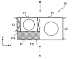
도 2는, 처리 유닛의 일례를 나타내는 도면이다.
도 3은, 도 2의 A 방향에서 본 처리 유닛의 일례를 나타내는 도면이다.
도 4는, 도 2의 B 방향에서 본 처리 유닛의 일례를 나타내는 도면이다.
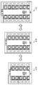
도 5는, 처리 유닛의 수가 상이한 처리 시스템의 일례를 나타내는 도면이다.
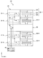
도 6은, 처리 유닛의 다른 예를 나타내는 도면이다.
도 7은, 처리 유닛의 또 다른 예를 나타내는 도면이다.
11 : LM
12 : 반송실
13 : 반송 장치
14 : 전원 유닛
20 : 처리 유닛
21 : LLM
210 : 게이트 밸브
211 : 반송 장치
212 : 게이트 밸브
22 : 처리 챔버
220 : 정합기
221 : 샤워 헤드
222 : 배치대
23 : 간극
230 : 배관
231 : 배관
232 : 배관
233 : 배관
234 : 배관
30 : 유틸리티 모듈
31 : 유량 제어부
32 : 배기 밸브
33 : 리모트 플라즈마 생성부
34 : 배기 펌프
40 : 가스 공급원
41 : 배기 장치
42 : 배기 가스 처리 장치
Claims (11)
을 구비하는 처리 시스템으로서, 각각의 상기 처리 유닛은,
공급된 처리 가스를 이용하여 피처리체를 처리하는 복수의 처리 챔버와,
상기 복수의 처리 챔버 각각에 공급되는 상기 처리 가스의 유량을 제어하는 유량 제어부를 포함하는 유틸리티 모듈
을 가지며,
상기 복수의 처리 챔버는, 상하 방향으로 중복되게 배치되고,
상기 유틸리티 모듈은, 상기 복수의 처리 챔버 중, 상하 방향으로 인접하는 2개의 처리 챔버 사이에 배치되는 것을 특징으로 하는 처리 시스템.
각각의 상기 처리 유닛은, 상기 유량 제어부로부터 상기 복수의 처리 챔버 각각에 분배되는 상기 처리 가스가 유통하는 제1 배관을 가지며,
상기 유량 제어부로부터 상기 복수의 처리 챔버 각각으로의 상기 제1 배관의 길이는, 상기 처리 유닛 내의 상기 복수의 처리 챔버들 간에 동일한 것을 특징으로 하는 처리 시스템.
각각의 상기 처리 유닛은, 상기 처리 챔버마다, 상기 처리 챔버에 인접하게 배치된 로드록 모듈(load lock module)을 가지며,
상기 로드록 모듈로부터 상기 처리 챔버로 향하는 방향에 있어서, 상기 로드록 모듈의 폭은, 상기 로드록 모듈에 인접하게 배치된 상기 처리 챔버의 폭보다 좁고,
상기 제1 배관은, 상기 로드록 모듈이 배치된 쪽의 상기 처리 챔버의 측면 중, 상기 로드록 모듈에 인접하지 않는 영역의 측면과, 상기 로드록 모듈의 측면 중, 상기 로드록 모듈로부터 상기 처리 챔버로 향하는 방향으로 연장되는 측면으로 형성된 간극에 배치되는 것을 특징으로 하는 처리 시스템.
상기 유틸리티 모듈은, 상기 처리 유닛이 갖는 상기 복수의 처리 챔버 각각으로부터 배기되는 가스의 배기량을 제어하는 배기 제어부를 더 갖는 것을 특징으로 하는 처리 시스템.
각각의 상기 처리 유닛은, 상기 복수의 처리 챔버 각각으로부터 배기되는 가스가 유통하는 제2 배관을 가지며,
상기 복수의 처리 챔버 각각으로부터 상기 배기 제어부까지의 상기 제2 배관의 길이는, 상기 처리 유닛 내의 상기 복수의 처리 챔버들 간에 동일한 것을 특징으로 하는 처리 시스템.
상기 처리 유닛은, 상기 처리 챔버마다, 상기 처리 챔버에 인접하게 배치된 로드록 모듈을 가지며,
상기 로드록 모듈로부터 상기 처리 챔버로 향하는 방향에 있어서, 상기 로드록 모듈의 폭은, 상기 로드록 모듈에 인접하게 배치된 상기 처리 챔버의 폭보다 좁고,
상기 제2 배관은, 상기 로드록 모듈이 배치된 쪽의 상기 처리 챔버의 측면 중, 상기 로드록 모듈에 인접하지 않는 영역의 측면과, 상기 로드록 모듈의 측면 중, 상기 로드록 모듈로부터 상기 처리 챔버로 향하는 방향으로 연장되는 측면으로 형성된 간극에 배치되는 것을 특징으로 하는 처리 시스템.
상기 유틸리티 모듈은, 플라즈마를 생성하고, 생성된 플라즈마 중의 라디칼을, 상기 처리 유닛이 갖는 상기 복수의 처리 챔버 각각에 공급하는 리모트 플라즈마 생성부를 더 갖는 것을 특징으로 하는 처리 시스템.
각각의 상기 처리 유닛은, 상기 리모트 플라즈마 생성부에 의해 생성되고, 상기 복수의 처리 챔버 각각에 분배되는 라디칼이 유통하는 제3 배관을 가지며,
상기 복수의 처리 챔버 각각으로부터 상기 리모트 플라즈마 생성부까지의 상기 제3 배관의 길이는, 상기 처리 유닛 내의 상기 복수의 처리 챔버들 간에 동일한 것을 특징으로 하는 처리 시스템.
각각의 상기 처리 유닛은, 상기 처리 챔버마다, 상기 처리 챔버에 인접하게 배치된 로드록 모듈을 가지며,
상기 로드록 모듈로부터 상기 처리 챔버로 향하는 방향에 있어서, 상기 로드록 모듈의 폭은, 상기 로드록 모듈에 인접하게 배치된 상기 처리 챔버의 폭보다 좁고,
상기 제3 배관은, 상기 로드록 모듈이 배치된 쪽의 상기 처리 챔버의 측면 중, 상기 로드록 모듈에 인접하지 않는 영역의 측면과, 상기 로드록 모듈의 측면 중, 상기 로드록 모듈로부터 상기 처리 챔버로 향하는 방향으로 연장되는 측면으로 형성된 간극에 배치되는 것을 특징으로 하는 처리 시스템.
상기 유틸리티 모듈은, 상기 처리 유닛이 갖는 상기 복수의 처리 챔버의 수를 n으로 한 경우에, 위로부터 n/2번째의 처리 챔버와 위로부터 (n/2)+1번째의 처리 챔버 사이에 배치되는 것을 특징으로 하는 처리 시스템.
Applications Claiming Priority (3)
| Application Number | Priority Date | Filing Date | Title |
|---|---|---|---|
| JPJP-P-2015-103896 | 2015-05-21 | ||
| JP2015103896A JP6463220B2 (ja) | 2015-05-21 | 2015-05-21 | 処理システム |
| PCT/JP2016/064066 WO2016185984A1 (ja) | 2015-05-21 | 2016-05-11 | 処理システム |
Publications (2)
| Publication Number | Publication Date |
|---|---|
| KR20170137196A true KR20170137196A (ko) | 2017-12-12 |
| KR102110021B1 KR102110021B1 (ko) | 2020-05-12 |
Family
ID=57320141
Family Applications (1)
| Application Number | Title | Priority Date | Filing Date |
|---|---|---|---|
| KR1020177033083A Active KR102110021B1 (ko) | 2015-05-21 | 2016-05-11 | 처리 시스템 |
Country Status (6)
| Country | Link |
|---|---|
| US (1) | US20180130681A1 (ko) |
| JP (1) | JP6463220B2 (ko) |
| KR (1) | KR102110021B1 (ko) |
| CN (1) | CN107615446B (ko) |
| TW (1) | TWI698551B (ko) |
| WO (1) | WO2016185984A1 (ko) |
Cited By (1)
| Publication number | Priority date | Publication date | Assignee | Title |
|---|---|---|---|---|
| US11387127B2 (en) | 2019-07-17 | 2022-07-12 | Semes Co., Ltd. | Substrate treating apparatus and substrate transfer apparatus |
Families Citing this family (3)
| Publication number | Priority date | Publication date | Assignee | Title |
|---|---|---|---|---|
| JP6844263B2 (ja) * | 2017-01-05 | 2021-03-17 | 東京エレクトロン株式会社 | 基板処理装置 |
| GB201718752D0 (en) | 2017-11-13 | 2017-12-27 | Edwards Ltd | Vacuum and abatement systems |
| CN119605614B (zh) * | 2024-11-21 | 2025-11-21 | 中国农业科学院西部农业研究中心 | 一种微咸水加菌滴灌系统及方法及计算机可读存储介质 |
Citations (2)
| Publication number | Priority date | Publication date | Assignee | Title |
|---|---|---|---|---|
| JPH10229111A (ja) * | 1997-02-18 | 1998-08-25 | Hitachi Ltd | 半導体製造装置 |
| JP2000223425A (ja) | 1999-02-02 | 2000-08-11 | Nec Corp | 基板処理装置、ガス供給方法、及び、レーザ光供給方法 |
Family Cites Families (16)
| Publication number | Priority date | Publication date | Assignee | Title |
|---|---|---|---|---|
| JPS6063374A (ja) * | 1983-09-14 | 1985-04-11 | Canon Inc | 気相法堆積膜製造装置 |
| US6176667B1 (en) * | 1996-04-30 | 2001-01-23 | Applied Materials, Inc. | Multideck wafer processing system |
| KR100269097B1 (ko) * | 1996-08-05 | 2000-12-01 | 엔도 마코토 | 기판처리장치 |
| US6835278B2 (en) * | 2000-07-07 | 2004-12-28 | Mattson Technology Inc. | Systems and methods for remote plasma clean |
| US6630053B2 (en) * | 2000-08-22 | 2003-10-07 | Asm Japan K.K. | Semiconductor processing module and apparatus |
| US20030045098A1 (en) * | 2001-08-31 | 2003-03-06 | Applied Materials, Inc. | Method and apparatus for processing a wafer |
| US6913652B2 (en) * | 2002-06-17 | 2005-07-05 | Applied Materials, Inc. | Gas flow division in a wafer processing system having multiple chambers |
| JP5025609B2 (ja) * | 2003-09-04 | 2012-09-12 | 株式会社日立ハイテクノロジーズ | 真空処理装置 |
| US20060104799A1 (en) * | 2004-07-12 | 2006-05-18 | Applied Materials, Inc. | Methods and apparatus for reducing an electronic device manufacturing tool footprint |
| JP2009105081A (ja) * | 2007-10-19 | 2009-05-14 | Ebatekku:Kk | 基板処理装置 |
| JP5260981B2 (ja) * | 2008-02-22 | 2013-08-14 | 株式会社日立ハイテクノロジーズ | 真空処理装置 |
| JP2011077399A (ja) * | 2009-09-30 | 2011-04-14 | Tokyo Electron Ltd | 被処理体の搬送方法及び被処理体処理装置 |
| TWI719331B (zh) * | 2011-10-26 | 2021-02-21 | 美商布魯克斯自動機械公司 | 基板處理系統 |
| US20150030766A1 (en) * | 2013-07-25 | 2015-01-29 | Novellus Systems, Inc. | Pedestal bottom clean for improved fluorine utilization and integrated symmetric foreline |
| JP2015035460A (ja) * | 2013-08-08 | 2015-02-19 | 信越半導体株式会社 | エピタキシャルウェーハの製造方法 |
| JP5977729B2 (ja) * | 2013-11-14 | 2016-08-24 | 東京エレクトロン株式会社 | 基板処理システム |
-
2015
- 2015-05-21 JP JP2015103896A patent/JP6463220B2/ja active Active
-
2016
- 2016-05-11 WO PCT/JP2016/064066 patent/WO2016185984A1/ja not_active Ceased
- 2016-05-11 US US15/574,514 patent/US20180130681A1/en not_active Abandoned
- 2016-05-11 CN CN201680029129.2A patent/CN107615446B/zh active Active
- 2016-05-11 KR KR1020177033083A patent/KR102110021B1/ko active Active
- 2016-05-17 TW TW105115209A patent/TWI698551B/zh not_active IP Right Cessation
Patent Citations (2)
| Publication number | Priority date | Publication date | Assignee | Title |
|---|---|---|---|---|
| JPH10229111A (ja) * | 1997-02-18 | 1998-08-25 | Hitachi Ltd | 半導体製造装置 |
| JP2000223425A (ja) | 1999-02-02 | 2000-08-11 | Nec Corp | 基板処理装置、ガス供給方法、及び、レーザ光供給方法 |
Cited By (1)
| Publication number | Priority date | Publication date | Assignee | Title |
|---|---|---|---|---|
| US11387127B2 (en) | 2019-07-17 | 2022-07-12 | Semes Co., Ltd. | Substrate treating apparatus and substrate transfer apparatus |
Also Published As
| Publication number | Publication date |
|---|---|
| TW201706450A (zh) | 2017-02-16 |
| CN107615446A (zh) | 2018-01-19 |
| KR102110021B1 (ko) | 2020-05-12 |
| WO2016185984A1 (ja) | 2016-11-24 |
| JP6463220B2 (ja) | 2019-01-30 |
| TWI698551B (zh) | 2020-07-11 |
| US20180130681A1 (en) | 2018-05-10 |
| JP2016219629A (ja) | 2016-12-22 |
| CN107615446B (zh) | 2020-12-04 |
Similar Documents
| Publication | Publication Date | Title |
|---|---|---|
| KR102073485B1 (ko) | 처리 장치 및 처리 방법 | |
| US10550469B2 (en) | Plasma excitation for spatial atomic layer deposition (ALD) reactors | |
| KR20170137196A (ko) | 처리 시스템 | |
| US11488810B2 (en) | Showerhead shroud | |
| KR102125122B1 (ko) | 기판 처리 장치 | |
| CN115206765B (zh) | 用于晶片放气的等离子体增强退火腔室 | |
| US11282737B2 (en) | Moving substrate transfer chamber | |
| KR20190023560A (ko) | 기판처리장치 및 그 세정방법 | |
| CN116397217A (zh) | 远程等离子体单元及包括其的衬底处理设备 | |
| KR101928008B1 (ko) | 기판 처리 장치 및 기판 처리 방법 | |
| KR20180021337A (ko) | 기판 처리 장치 및 기판 처리 방법 | |
| JP7450159B2 (ja) | 基板処理装置 | |
| JP2022018902A (ja) | 基板処理システム、メンテナンス方法及び基板処理方法 | |
| US12562356B2 (en) | Linear arrangement for substrate processing tools | |
| JP2024019926A (ja) | 成膜装置 | |
| KR20250087820A (ko) | 통합 처리 장치 | |
| KR20190084659A (ko) | 기판 처리 장치 | |
| KR20060066407A (ko) | 통합 진공 펌프를 갖는 반도체 제조 장치 |
Legal Events
| Date | Code | Title | Description |
|---|---|---|---|
| A201 | Request for examination | ||
| PA0105 | International application |
St.27 status event code: A-0-1-A10-A15-nap-PA0105 |
|
| PA0201 | Request for examination |
St.27 status event code: A-1-2-D10-D11-exm-PA0201 |
|
| PG1501 | Laying open of application |
St.27 status event code: A-1-1-Q10-Q12-nap-PG1501 |
|
| E902 | Notification of reason for refusal | ||
| PE0902 | Notice of grounds for rejection |
St.27 status event code: A-1-2-D10-D21-exm-PE0902 |
|
| E13-X000 | Pre-grant limitation requested |
St.27 status event code: A-2-3-E10-E13-lim-X000 |
|
| P11-X000 | Amendment of application requested |
St.27 status event code: A-2-2-P10-P11-nap-X000 |
|
| P13-X000 | Application amended |
St.27 status event code: A-2-2-P10-P13-nap-X000 |
|
| E90F | Notification of reason for final refusal | ||
| PE0902 | Notice of grounds for rejection |
St.27 status event code: A-1-2-D10-D21-exm-PE0902 |
|
| P11-X000 | Amendment of application requested |
St.27 status event code: A-2-2-P10-P11-nap-X000 |
|
| P13-X000 | Application amended |
St.27 status event code: A-2-2-P10-P13-nap-X000 |
|
| E701 | Decision to grant or registration of patent right | ||
| PE0701 | Decision of registration |
St.27 status event code: A-1-2-D10-D22-exm-PE0701 |
|
| GRNT | Written decision to grant | ||
| PR0701 | Registration of establishment |
St.27 status event code: A-2-4-F10-F11-exm-PR0701 |
|
| PR1002 | Payment of registration fee |
St.27 status event code: A-2-2-U10-U12-oth-PR1002 Fee payment year number: 1 |
|
| PG1601 | Publication of registration |
St.27 status event code: A-4-4-Q10-Q13-nap-PG1601 |
|
| PR1001 | Payment of annual fee |
St.27 status event code: A-4-4-U10-U11-oth-PR1001 Fee payment year number: 4 |
|
| PR1001 | Payment of annual fee |
St.27 status event code: A-4-4-U10-U11-oth-PR1001 Fee payment year number: 5 |
|
| PR1001 | Payment of annual fee |
St.27 status event code: A-4-4-U10-U11-oth-PR1001 Fee payment year number: 6 |
|
| P22-X000 | Classification modified |
St.27 status event code: A-4-4-P10-P22-nap-X000 |
|
| PR1001 | Payment of annual fee |
St.27 status event code: A-4-4-U10-U11-oth-PR1001 Fee payment year number: 7 |
|
| U11 | Full renewal or maintenance fee paid |
Free format text: ST27 STATUS EVENT CODE: A-4-4-U10-U11-OTH-PR1001 (AS PROVIDED BY THE NATIONAL OFFICE) Year of fee payment: 7 |