KR20180109708A - 적층체 및 그의 제조 방법 - Google Patents
적층체 및 그의 제조 방법 Download PDFInfo
- Publication number
- KR20180109708A KR20180109708A KR1020180033004A KR20180033004A KR20180109708A KR 20180109708 A KR20180109708 A KR 20180109708A KR 1020180033004 A KR1020180033004 A KR 1020180033004A KR 20180033004 A KR20180033004 A KR 20180033004A KR 20180109708 A KR20180109708 A KR 20180109708A
- Authority
- KR
- South Korea
- Prior art keywords
- layer
- resin
- forming
- group
- trade name
- Prior art date
- Legal status (The legal status is an assumption and is not a legal conclusion. Google has not performed a legal analysis and makes no representation as to the accuracy of the status listed.)
- Granted
Links
Classifications
-
- H—ELECTRICITY
- H10—SEMICONDUCTOR DEVICES; ELECTRIC SOLID-STATE DEVICES NOT OTHERWISE PROVIDED FOR
- H10W—GENERIC PACKAGES, INTERCONNECTIONS, CONNECTORS OR OTHER CONSTRUCTIONAL DETAILS OF DEVICES COVERED BY CLASS H10
- H10W70/00—Package substrates; Interposers; Redistribution layers [RDL]
- H10W70/60—Insulating or insulated package substrates; Interposers; Redistribution layers
- H10W70/62—Insulating or insulated package substrates; Interposers; Redistribution layers characterised by their interconnections
- H10W70/65—Shapes or dispositions of interconnections
-
- B—PERFORMING OPERATIONS; TRANSPORTING
- B32—LAYERED PRODUCTS
- B32B—LAYERED PRODUCTS, i.e. PRODUCTS BUILT-UP OF STRATA OF FLAT OR NON-FLAT, e.g. CELLULAR OR HONEYCOMB, FORM
- B32B15/00—Layered products comprising a layer of metal
-
- B—PERFORMING OPERATIONS; TRANSPORTING
- B32—LAYERED PRODUCTS
- B32B—LAYERED PRODUCTS, i.e. PRODUCTS BUILT-UP OF STRATA OF FLAT OR NON-FLAT, e.g. CELLULAR OR HONEYCOMB, FORM
- B32B15/00—Layered products comprising a layer of metal
- B32B15/04—Layered products comprising a layer of metal comprising metal as the main or only constituent of a layer, which is next to another layer of the same or of a different material
- B32B15/08—Layered products comprising a layer of metal comprising metal as the main or only constituent of a layer, which is next to another layer of the same or of a different material of synthetic resin
-
- B—PERFORMING OPERATIONS; TRANSPORTING
- B32—LAYERED PRODUCTS
- B32B—LAYERED PRODUCTS, i.e. PRODUCTS BUILT-UP OF STRATA OF FLAT OR NON-FLAT, e.g. CELLULAR OR HONEYCOMB, FORM
- B32B15/00—Layered products comprising a layer of metal
- B32B15/04—Layered products comprising a layer of metal comprising metal as the main or only constituent of a layer, which is next to another layer of the same or of a different material
- B32B15/08—Layered products comprising a layer of metal comprising metal as the main or only constituent of a layer, which is next to another layer of the same or of a different material of synthetic resin
- B32B15/092—Layered products comprising a layer of metal comprising metal as the main or only constituent of a layer, which is next to another layer of the same or of a different material of synthetic resin comprising epoxy resins
-
- B—PERFORMING OPERATIONS; TRANSPORTING
- B32—LAYERED PRODUCTS
- B32B—LAYERED PRODUCTS, i.e. PRODUCTS BUILT-UP OF STRATA OF FLAT OR NON-FLAT, e.g. CELLULAR OR HONEYCOMB, FORM
- B32B15/00—Layered products comprising a layer of metal
- B32B15/20—Layered products comprising a layer of metal comprising aluminium or copper
-
- B—PERFORMING OPERATIONS; TRANSPORTING
- B32—LAYERED PRODUCTS
- B32B—LAYERED PRODUCTS, i.e. PRODUCTS BUILT-UP OF STRATA OF FLAT OR NON-FLAT, e.g. CELLULAR OR HONEYCOMB, FORM
- B32B27/00—Layered products comprising a layer of synthetic resin
- B32B27/06—Layered products comprising a layer of synthetic resin as the main or only constituent of a layer, which is next to another layer of the same or of a different material
-
- B—PERFORMING OPERATIONS; TRANSPORTING
- B32—LAYERED PRODUCTS
- B32B—LAYERED PRODUCTS, i.e. PRODUCTS BUILT-UP OF STRATA OF FLAT OR NON-FLAT, e.g. CELLULAR OR HONEYCOMB, FORM
- B32B27/00—Layered products comprising a layer of synthetic resin
- B32B27/28—Layered products comprising a layer of synthetic resin comprising synthetic resins not wholly covered by any one of the sub-groups B32B27/30 - B32B27/42
-
- B—PERFORMING OPERATIONS; TRANSPORTING
- B32—LAYERED PRODUCTS
- B32B—LAYERED PRODUCTS, i.e. PRODUCTS BUILT-UP OF STRATA OF FLAT OR NON-FLAT, e.g. CELLULAR OR HONEYCOMB, FORM
- B32B27/00—Layered products comprising a layer of synthetic resin
- B32B27/28—Layered products comprising a layer of synthetic resin comprising synthetic resins not wholly covered by any one of the sub-groups B32B27/30 - B32B27/42
- B32B27/281—Layered products comprising a layer of synthetic resin comprising synthetic resins not wholly covered by any one of the sub-groups B32B27/30 - B32B27/42 comprising polyimides
-
- B—PERFORMING OPERATIONS; TRANSPORTING
- B32—LAYERED PRODUCTS
- B32B—LAYERED PRODUCTS, i.e. PRODUCTS BUILT-UP OF STRATA OF FLAT OR NON-FLAT, e.g. CELLULAR OR HONEYCOMB, FORM
- B32B27/00—Layered products comprising a layer of synthetic resin
- B32B27/38—Layered products comprising a layer of synthetic resin comprising epoxy resins
-
- C—CHEMISTRY; METALLURGY
- C08—ORGANIC MACROMOLECULAR COMPOUNDS; THEIR PREPARATION OR CHEMICAL WORKING-UP; COMPOSITIONS BASED THEREON
- C08G—MACROMOLECULAR COMPOUNDS OBTAINED OTHERWISE THAN BY REACTIONS ONLY INVOLVING UNSATURATED CARBON-TO-CARBON BONDS
- C08G8/00—Condensation polymers of aldehydes or ketones with phenols only
- C08G8/04—Condensation polymers of aldehydes or ketones with phenols only of aldehydes
-
- C—CHEMISTRY; METALLURGY
- C08—ORGANIC MACROMOLECULAR COMPOUNDS; THEIR PREPARATION OR CHEMICAL WORKING-UP; COMPOSITIONS BASED THEREON
- C08L—COMPOSITIONS OF MACROMOLECULAR COMPOUNDS
- C08L63/00—Compositions of epoxy resins; Compositions of derivatives of epoxy resins
-
- C—CHEMISTRY; METALLURGY
- C08—ORGANIC MACROMOLECULAR COMPOUNDS; THEIR PREPARATION OR CHEMICAL WORKING-UP; COMPOSITIONS BASED THEREON
- C08L—COMPOSITIONS OF MACROMOLECULAR COMPOUNDS
- C08L65/00—Compositions of macromolecular compounds obtained by reactions forming a carbon-to-carbon link in the main chain; Compositions of derivatives of such polymers
-
- C—CHEMISTRY; METALLURGY
- C09—DYES; PAINTS; POLISHES; NATURAL RESINS; ADHESIVES; COMPOSITIONS NOT OTHERWISE PROVIDED FOR; APPLICATIONS OF MATERIALS NOT OTHERWISE PROVIDED FOR
- C09D—COATING COMPOSITIONS, e.g. PAINTS, VARNISHES OR LACQUERS; FILLING PASTES; CHEMICAL PAINT OR INK REMOVERS; INKS; CORRECTING FLUIDS; WOODSTAINS; PASTES OR SOLIDS FOR COLOURING OR PRINTING; USE OF MATERIALS THEREFOR
- C09D161/00—Coating compositions based on condensation polymers of aldehydes or ketones; Coating compositions based on derivatives of such polymers
- C09D161/04—Condensation polymers of aldehydes or ketones with phenols only
- C09D161/06—Condensation polymers of aldehydes or ketones with phenols only of aldehydes with phenols
- C09D161/12—Condensation polymers of aldehydes or ketones with phenols only of aldehydes with phenols with polyhydric phenols
-
- H01L21/563—
-
- H01L23/485—
-
- H—ELECTRICITY
- H10—SEMICONDUCTOR DEVICES; ELECTRIC SOLID-STATE DEVICES NOT OTHERWISE PROVIDED FOR
- H10P—GENERIC PROCESSES OR APPARATUS FOR THE MANUFACTURE OR TREATMENT OF DEVICES COVERED BY CLASS H10
- H10P72/00—Handling or holding of wafers, substrates or devices during manufacture or treatment thereof
- H10P72/70—Handling or holding of wafers, substrates or devices during manufacture or treatment thereof for supporting or gripping
-
- H—ELECTRICITY
- H10—SEMICONDUCTOR DEVICES; ELECTRIC SOLID-STATE DEVICES NOT OTHERWISE PROVIDED FOR
- H10P—GENERIC PROCESSES OR APPARATUS FOR THE MANUFACTURE OR TREATMENT OF DEVICES COVERED BY CLASS H10
- H10P72/00—Handling or holding of wafers, substrates or devices during manufacture or treatment thereof
- H10P72/70—Handling or holding of wafers, substrates or devices during manufacture or treatment thereof for supporting or gripping
- H10P72/74—Handling or holding of wafers, substrates or devices during manufacture or treatment thereof for supporting or gripping using temporarily an auxiliary support
-
- H—ELECTRICITY
- H10—SEMICONDUCTOR DEVICES; ELECTRIC SOLID-STATE DEVICES NOT OTHERWISE PROVIDED FOR
- H10W—GENERIC PACKAGES, INTERCONNECTIONS, CONNECTORS OR OTHER CONSTRUCTIONAL DETAILS OF DEVICES COVERED BY CLASS H10
- H10W20/00—Interconnections in chips, wafers or substrates
- H10W20/40—Interconnections external to wafers or substrates, e.g. back-end-of-line [BEOL] metallisations or vias connecting to gate electrodes
-
- H—ELECTRICITY
- H10—SEMICONDUCTOR DEVICES; ELECTRIC SOLID-STATE DEVICES NOT OTHERWISE PROVIDED FOR
- H10W—GENERIC PACKAGES, INTERCONNECTIONS, CONNECTORS OR OTHER CONSTRUCTIONAL DETAILS OF DEVICES COVERED BY CLASS H10
- H10W70/00—Package substrates; Interposers; Redistribution layers [RDL]
- H10W70/01—Manufacture or treatment
- H10W70/05—Manufacture or treatment of insulating or insulated package substrates, or of interposers, or of redistribution layers
-
- H—ELECTRICITY
- H10—SEMICONDUCTOR DEVICES; ELECTRIC SOLID-STATE DEVICES NOT OTHERWISE PROVIDED FOR
- H10W—GENERIC PACKAGES, INTERCONNECTIONS, CONNECTORS OR OTHER CONSTRUCTIONAL DETAILS OF DEVICES COVERED BY CLASS H10
- H10W70/00—Package substrates; Interposers; Redistribution layers [RDL]
- H10W70/01—Manufacture or treatment
- H10W70/05—Manufacture or treatment of insulating or insulated package substrates, or of interposers, or of redistribution layers
- H10W70/08—Manufacture or treatment of insulating or insulated package substrates, or of interposers, or of redistribution layers by depositing layers on the chip or wafer, e.g. "chip-first" RDLs
- H10W70/09—Manufacture or treatment of insulating or insulated package substrates, or of interposers, or of redistribution layers by depositing layers on the chip or wafer, e.g. "chip-first" RDLs extending onto an encapsulation that laterally surrounds the chip or wafer, e.g. fan-out wafer level package [FOWLP] RDLs
-
- H—ELECTRICITY
- H10—SEMICONDUCTOR DEVICES; ELECTRIC SOLID-STATE DEVICES NOT OTHERWISE PROVIDED FOR
- H10W—GENERIC PACKAGES, INTERCONNECTIONS, CONNECTORS OR OTHER CONSTRUCTIONAL DETAILS OF DEVICES COVERED BY CLASS H10
- H10W72/00—Interconnections or connectors in packages
- H10W72/701—Tape-automated bond [TAB] connectors
-
- H—ELECTRICITY
- H10—SEMICONDUCTOR DEVICES; ELECTRIC SOLID-STATE DEVICES NOT OTHERWISE PROVIDED FOR
- H10W—GENERIC PACKAGES, INTERCONNECTIONS, CONNECTORS OR OTHER CONSTRUCTIONAL DETAILS OF DEVICES COVERED BY CLASS H10
- H10W74/00—Encapsulations, e.g. protective coatings
- H10W74/01—Manufacture or treatment
- H10W74/012—Manufacture or treatment of encapsulations on active surfaces of flip-chip devices, e.g. forming underfills
-
- B—PERFORMING OPERATIONS; TRANSPORTING
- B32—LAYERED PRODUCTS
- B32B—LAYERED PRODUCTS, i.e. PRODUCTS BUILT-UP OF STRATA OF FLAT OR NON-FLAT, e.g. CELLULAR OR HONEYCOMB, FORM
- B32B2457/00—Electrical equipment
- B32B2457/20—Displays, e.g. liquid crystal displays, plasma displays
-
- C—CHEMISTRY; METALLURGY
- C23—COATING METALLIC MATERIAL; COATING MATERIAL WITH METALLIC MATERIAL; CHEMICAL SURFACE TREATMENT; DIFFUSION TREATMENT OF METALLIC MATERIAL; COATING BY VACUUM EVAPORATION, BY SPUTTERING, BY ION IMPLANTATION OR BY CHEMICAL VAPOUR DEPOSITION, IN GENERAL; INHIBITING CORROSION OF METALLIC MATERIAL OR INCRUSTATION IN GENERAL
- C23C—COATING METALLIC MATERIAL; COATING MATERIAL WITH METALLIC MATERIAL; SURFACE TREATMENT OF METALLIC MATERIAL BY DIFFUSION INTO THE SURFACE, BY CHEMICAL CONVERSION OR SUBSTITUTION; COATING BY VACUUM EVAPORATION, BY SPUTTERING, BY ION IMPLANTATION OR BY CHEMICAL VAPOUR DEPOSITION, IN GENERAL
- C23C14/00—Coating by vacuum evaporation, by sputtering or by ion implantation of the coating forming material
- C23C14/06—Coating by vacuum evaporation, by sputtering or by ion implantation of the coating forming material characterised by the coating material
- C23C14/14—Metallic material, boron or silicon
- C23C14/20—Metallic material, boron or silicon on organic substrates
- C23C14/205—Metallic material, boron or silicon on organic substrates by cathodic sputtering
-
- C—CHEMISTRY; METALLURGY
- C23—COATING METALLIC MATERIAL; COATING MATERIAL WITH METALLIC MATERIAL; CHEMICAL SURFACE TREATMENT; DIFFUSION TREATMENT OF METALLIC MATERIAL; COATING BY VACUUM EVAPORATION, BY SPUTTERING, BY ION IMPLANTATION OR BY CHEMICAL VAPOUR DEPOSITION, IN GENERAL; INHIBITING CORROSION OF METALLIC MATERIAL OR INCRUSTATION IN GENERAL
- C23C—COATING METALLIC MATERIAL; COATING MATERIAL WITH METALLIC MATERIAL; SURFACE TREATMENT OF METALLIC MATERIAL BY DIFFUSION INTO THE SURFACE, BY CHEMICAL CONVERSION OR SUBSTITUTION; COATING BY VACUUM EVAPORATION, BY SPUTTERING, BY ION IMPLANTATION OR BY CHEMICAL VAPOUR DEPOSITION, IN GENERAL
- C23C14/00—Coating by vacuum evaporation, by sputtering or by ion implantation of the coating forming material
- C23C14/22—Coating by vacuum evaporation, by sputtering or by ion implantation of the coating forming material characterised by the process of coating
- C23C14/34—Sputtering
-
- C—CHEMISTRY; METALLURGY
- C25—ELECTROLYTIC OR ELECTROPHORETIC PROCESSES; APPARATUS THEREFOR
- C25D—PROCESSES FOR THE ELECTROLYTIC OR ELECTROPHORETIC PRODUCTION OF COATINGS; ELECTROFORMING; APPARATUS THEREFOR
- C25D3/00—Electroplating: Baths therefor
- C25D3/02—Electroplating: Baths therefor from solutions
- C25D3/38—Electroplating: Baths therefor from solutions of copper
-
- H—ELECTRICITY
- H10—SEMICONDUCTOR DEVICES; ELECTRIC SOLID-STATE DEVICES NOT OTHERWISE PROVIDED FOR
- H10P—GENERIC PROCESSES OR APPARATUS FOR THE MANUFACTURE OR TREATMENT OF DEVICES COVERED BY CLASS H10
- H10P72/00—Handling or holding of wafers, substrates or devices during manufacture or treatment thereof
- H10P72/70—Handling or holding of wafers, substrates or devices during manufacture or treatment thereof for supporting or gripping
- H10P72/74—Handling or holding of wafers, substrates or devices during manufacture or treatment thereof for supporting or gripping using temporarily an auxiliary support
- H10P72/7412—Handling or holding of wafers, substrates or devices during manufacture or treatment thereof for supporting or gripping using temporarily an auxiliary support the auxiliary support including means facilitating the separation of a device or wafer from the auxiliary support
-
- H—ELECTRICITY
- H10—SEMICONDUCTOR DEVICES; ELECTRIC SOLID-STATE DEVICES NOT OTHERWISE PROVIDED FOR
- H10P—GENERIC PROCESSES OR APPARATUS FOR THE MANUFACTURE OR TREATMENT OF DEVICES COVERED BY CLASS H10
- H10P72/00—Handling or holding of wafers, substrates or devices during manufacture or treatment thereof
- H10P72/70—Handling or holding of wafers, substrates or devices during manufacture or treatment thereof for supporting or gripping
- H10P72/74—Handling or holding of wafers, substrates or devices during manufacture or treatment thereof for supporting or gripping using temporarily an auxiliary support
- H10P72/7424—Handling or holding of wafers, substrates or devices during manufacture or treatment thereof for supporting or gripping using temporarily an auxiliary support used as a support during the manufacture of self-supporting substrates
-
- H—ELECTRICITY
- H10—SEMICONDUCTOR DEVICES; ELECTRIC SOLID-STATE DEVICES NOT OTHERWISE PROVIDED FOR
- H10W—GENERIC PACKAGES, INTERCONNECTIONS, CONNECTORS OR OTHER CONSTRUCTIONAL DETAILS OF DEVICES COVERED BY CLASS H10
- H10W70/00—Package substrates; Interposers; Redistribution layers [RDL]
- H10W70/01—Manufacture or treatment
- H10W70/05—Manufacture or treatment of insulating or insulated package substrates, or of interposers, or of redistribution layers
- H10W70/093—Connecting or disconnecting other interconnections thereto or therefrom, e.g. connecting bond wires or bumps
-
- H—ELECTRICITY
- H10—SEMICONDUCTOR DEVICES; ELECTRIC SOLID-STATE DEVICES NOT OTHERWISE PROVIDED FOR
- H10W—GENERIC PACKAGES, INTERCONNECTIONS, CONNECTORS OR OTHER CONSTRUCTIONAL DETAILS OF DEVICES COVERED BY CLASS H10
- H10W70/00—Package substrates; Interposers; Redistribution layers [RDL]
- H10W70/60—Insulating or insulated package substrates; Interposers; Redistribution layers
-
- H—ELECTRICITY
- H10—SEMICONDUCTOR DEVICES; ELECTRIC SOLID-STATE DEVICES NOT OTHERWISE PROVIDED FOR
- H10W—GENERIC PACKAGES, INTERCONNECTIONS, CONNECTORS OR OTHER CONSTRUCTIONAL DETAILS OF DEVICES COVERED BY CLASS H10
- H10W70/00—Package substrates; Interposers; Redistribution layers [RDL]
- H10W70/60—Insulating or insulated package substrates; Interposers; Redistribution layers
- H10W70/62—Insulating or insulated package substrates; Interposers; Redistribution layers characterised by their interconnections
- H10W70/66—Conductive materials thereof
-
- H—ELECTRICITY
- H10—SEMICONDUCTOR DEVICES; ELECTRIC SOLID-STATE DEVICES NOT OTHERWISE PROVIDED FOR
- H10W—GENERIC PACKAGES, INTERCONNECTIONS, CONNECTORS OR OTHER CONSTRUCTIONAL DETAILS OF DEVICES COVERED BY CLASS H10
- H10W74/00—Encapsulations, e.g. protective coatings
- H10W74/10—Encapsulations, e.g. protective coatings characterised by their shape or disposition
- H10W74/15—Encapsulations, e.g. protective coatings characterised by their shape or disposition on active surfaces of flip-chip devices, e.g. underfills
-
- H—ELECTRICITY
- H10—SEMICONDUCTOR DEVICES; ELECTRIC SOLID-STATE DEVICES NOT OTHERWISE PROVIDED FOR
- H10W—GENERIC PACKAGES, INTERCONNECTIONS, CONNECTORS OR OTHER CONSTRUCTIONAL DETAILS OF DEVICES COVERED BY CLASS H10
- H10W90/00—Package configurations
- H10W90/701—Package configurations characterised by the relative positions of pads or connectors relative to package parts
- H10W90/721—Package configurations characterised by the relative positions of pads or connectors relative to package parts of bump connectors
- H10W90/724—Package configurations characterised by the relative positions of pads or connectors relative to package parts of bump connectors between a chip and a stacked insulating package substrate, interposer or RDL
-
- H—ELECTRICITY
- H10—SEMICONDUCTOR DEVICES; ELECTRIC SOLID-STATE DEVICES NOT OTHERWISE PROVIDED FOR
- H10W—GENERIC PACKAGES, INTERCONNECTIONS, CONNECTORS OR OTHER CONSTRUCTIONAL DETAILS OF DEVICES COVERED BY CLASS H10
- H10W90/00—Package configurations
- H10W90/701—Package configurations characterised by the relative positions of pads or connectors relative to package parts
- H10W90/731—Package configurations characterised by the relative positions of pads or connectors relative to package parts of die-attach connectors
- H10W90/734—Package configurations characterised by the relative positions of pads or connectors relative to package parts of die-attach connectors between a chip and a stacked insulating package substrate, interposer or RDL
Landscapes
- Chemical & Material Sciences (AREA)
- Organic Chemistry (AREA)
- Health & Medical Sciences (AREA)
- Chemical Kinetics & Catalysis (AREA)
- Medicinal Chemistry (AREA)
- Polymers & Plastics (AREA)
- Engineering & Computer Science (AREA)
- Life Sciences & Earth Sciences (AREA)
- Materials Engineering (AREA)
- Wood Science & Technology (AREA)
- Laminated Bodies (AREA)
- Phenolic Resins Or Amino Resins (AREA)
- Manufacturing Of Printed Wiring (AREA)
- Internal Circuitry In Semiconductor Integrated Circuit Devices (AREA)
- Physics & Mathematics (AREA)
- Geometry (AREA)
- Ceramic Engineering (AREA)
- Adhesives Or Adhesive Processes (AREA)
- Compositions Of Macromolecular Compounds (AREA)
- Manufacturing & Machinery (AREA)
Abstract
[해결 수단] 지지체와, 해당 지지체 상에 형성된 광 조사에 의해 분해 가능한 차광성 수지를 포함하는 수지층과, 해당 수지층 상에 형성된 금속층과, 해당 금속층 상에 형성된 절연층 및 재배선층을 구비하는 적층체이며, 상기 수지층의 파장 355nm의 광 투과율이 20% 이하인 적층체.
Description




Claims (7)
- 지지체와, 해당 지지체 상에 형성된 광 조사에 의해 분해 가능한 차광성 수지를 포함하는 수지층과, 해당 수지층 상에 형성된 금속층과, 해당 금속층 상에 형성된 절연층 및 재배선층을 구비하는 적층체이며, 상기 수지층의 파장 355nm의 광 투과율이 20% 이하인 적층체.
- 제1항에 있어서, 상기 금속층이 티타늄, 알루미늄, 구리, 텅스텐, 탄탈륨, 몰리브덴, 크롬, 니오븀 및 금으로부터 선택되는 적어도 1종의 금속을 포함하는 적층체.
- 제2항에 있어서, 상기 금속층이 티타늄, 알루미늄, 구리 및 티타늄과 텅스텐의 합금으로부터 선택되는 적어도 하나를 포함하는 적층체.
- 제1항 내지 제3항 중 어느 한 항에 있어서, 상기 절연층이 벤조시클로부텐, 에폭시 수지, 폴리이미드 수지, 실리콘 수지 및 폴리벤조옥사졸로부터 선택되는 적어도 하나의 수지를 포함하는 적층체.
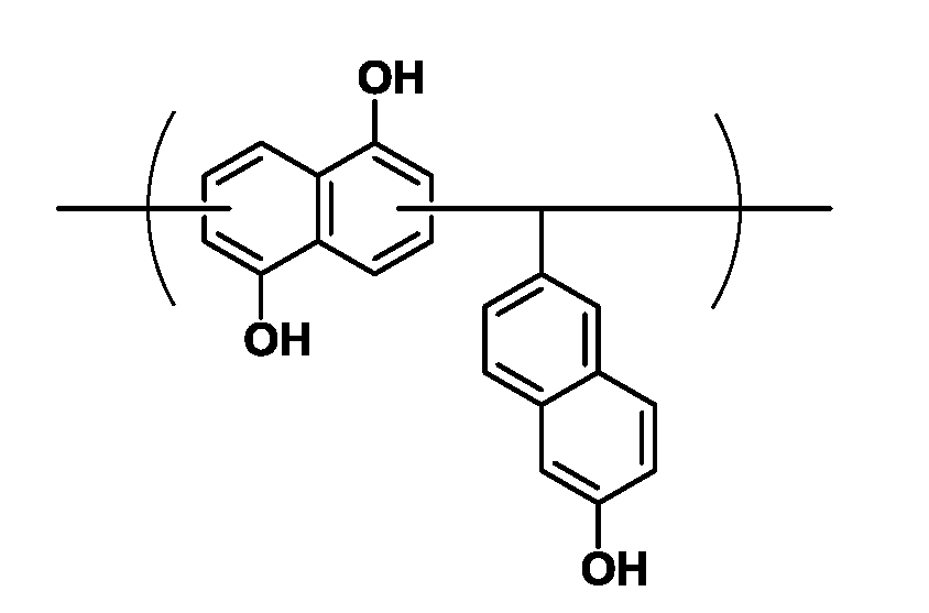
- 제1항 내지 제4항 중 어느 한 항에 있어서, 상기 차광성 수지가 주쇄에 축합환을 포함하는 수지인 적층체.
- 제1항 내지 제5항 중 어느 한 항에 있어서, 상기 수지층이 하기 식 (1)로 표시되는 반복 단위를 포함하는 수지 A를 포함하는 수지 조성물 A의 경화물을 포함하는 것인 적층체.

(식 중, R1 내지 R3은 각각 독립적으로 수소 원자, 히드록시기 또는 탄소수 1 내지 20의 1가의 유기기이지만, R1 내지 R3 중 적어도 하나는 히드록시기다. R4는 수소 원자, 또는 치환기를 갖고 있어도 되는 탄소수 1 내지 30의 1가의 유기기이다.) - (a) 지지체에 직접 수지층을 형성하는 공정,
(b) 상기 수지층 상에 금속층을 형성하는 공정,
(c) 상기 금속층 상에 절연층을 형성하고, 해당 절연층에 패턴을 형성하는 공정,
(d) 상기 패턴을 형성한 절연층 상에 도전층을 형성하는 공정,
(e) 상기 도전층 상에 도금 레지스트층을 형성하고, 해당 도금 레지스트층에 패턴을 형성하고, 상기 도금 레지스트층의 패턴 사이에 상기 도전층을 노출시키는 공정, 및
(f) 상기 도금 레지스트층의 패턴 사이에 노출된 도전층 상에 재배선층을 형성하는 공정
을 포함하는 제1항 내지 제6항 중 어느 한 항 기재된 적층체의 제조 방법.
Applications Claiming Priority (2)
| Application Number | Priority Date | Filing Date | Title |
|---|---|---|---|
| JPJP-P-2017-060663 | 2017-03-27 | ||
| JP2017060663A JP6743738B2 (ja) | 2017-03-27 | 2017-03-27 | 積層体及びその製造方法 |
Publications (2)
| Publication Number | Publication Date |
|---|---|
| KR20180109708A true KR20180109708A (ko) | 2018-10-08 |
| KR102476071B1 KR102476071B1 (ko) | 2022-12-12 |
Family
ID=61912944
Family Applications (1)
| Application Number | Title | Priority Date | Filing Date |
|---|---|---|---|
| KR1020180033004A Active KR102476071B1 (ko) | 2017-03-27 | 2018-03-22 | 적층체 및 그의 제조 방법 |
Country Status (6)
| Country | Link |
|---|---|
| US (1) | US10373903B2 (ko) |
| EP (1) | EP3382743B1 (ko) |
| JP (1) | JP6743738B2 (ko) |
| KR (1) | KR102476071B1 (ko) |
| CN (1) | CN108656662B (ko) |
| TW (1) | TWI787245B (ko) |
Families Citing this family (1)
| Publication number | Priority date | Publication date | Assignee | Title |
|---|---|---|---|---|
| JP6662337B2 (ja) * | 2017-03-27 | 2020-03-11 | 信越化学工業株式会社 | 半導体装置及びその製造方法、並びに積層体 |
Citations (9)
| Publication number | Priority date | Publication date | Assignee | Title |
|---|---|---|---|---|
| JP2003177528A (ja) | 2001-09-21 | 2003-06-27 | Tamura Kaken Co Ltd | 感光性樹脂組成物及びプリント配線板 |
| JP2013058520A (ja) | 2011-09-07 | 2013-03-28 | Dainippon Screen Mfg Co Ltd | 描画装置、データ補正装置、再配線層の形成方法、および、データ補正方法 |
| JP2013171949A (ja) * | 2012-02-20 | 2013-09-02 | Tokyo Ohka Kogyo Co Ltd | 支持体分離方法及び支持体分離装置 |
| KR20130128400A (ko) * | 2010-10-29 | 2013-11-26 | 도오꾜오까고오교 가부시끼가이샤 | 적층체, 및 그 적층체의 분리 방법 |
| KR20140072803A (ko) * | 2012-12-05 | 2014-06-13 | 도오꾜오까고오교 가부시끼가이샤 | 적층체의 형성 방법 |
| WO2015072418A1 (ja) | 2013-11-12 | 2015-05-21 | 信越化学工業株式会社 | シリコーン接着剤組成物及び固体撮像デバイス |
| JP2016111275A (ja) * | 2014-12-09 | 2016-06-20 | 凸版印刷株式会社 | 配線基板及びラミネート装置 |
| JP2016146402A (ja) | 2015-02-06 | 2016-08-12 | 凸版印刷株式会社 | 配線基板、半導体装置及び半導体装置の製造方法 |
| KR20160123959A (ko) * | 2015-04-17 | 2016-10-26 | 타이완 세미콘덕터 매뉴팩쳐링 컴퍼니 리미티드 | 팬아웃 상호 접속 구조 및 그 형성 방법 |
Family Cites Families (17)
| Publication number | Priority date | Publication date | Assignee | Title |
|---|---|---|---|---|
| JPS5243353A (en) | 1975-10-02 | 1977-04-05 | Matsushita Electric Ind Co Ltd | Timer circuit |
| US4378381A (en) | 1980-10-31 | 1983-03-29 | International Telephone And Telegraph Corporation | Suspensions containing microfibrillated cellulose |
| DE3590588T1 (de) * | 1984-11-09 | 1986-10-30 | Konica Corp., Tokio/Tokyo | Leitendes Verbundgebilde |
| EP1494073A3 (en) | 2001-09-21 | 2005-04-06 | Tamura Kaken Corporation | Photosensitive resin composition and printed wiring board |
| TW200602376A (en) * | 2004-05-21 | 2006-01-16 | Showa Denko Kk | Electroconductive composition and application thereof |
| JP2007242888A (ja) * | 2006-03-08 | 2007-09-20 | Sony Corp | 半導体パッケージ製造方法 |
| WO2010109861A1 (ja) * | 2009-03-27 | 2010-09-30 | 三菱瓦斯化学株式会社 | 樹脂溶液の保存方法、並びに、プリプレグ及び積層板の製造方法 |
| TWI516527B (zh) | 2009-12-10 | 2016-01-11 | 信越化學工業股份有限公司 | 光固化性樹脂組成物,圖案形成法和基板保護膜,以及使用該組成物之膜狀黏著劑及黏著片 |
| JP5579764B2 (ja) | 2012-03-05 | 2014-08-27 | 信越化学工業株式会社 | アンダーフィル用液状エポキシ樹脂組成物、及び該組成物で封止された半導体装置 |
| JP6222428B2 (ja) * | 2013-07-05 | 2017-11-01 | ナガセケムテックス株式会社 | エポキシ樹脂組成物 |
| JP6099815B2 (ja) * | 2013-10-04 | 2017-03-22 | アクロン ポリマー システムズ,インク. | 電子装置を製造する方法 |
| KR102352289B1 (ko) * | 2014-04-17 | 2022-01-19 | 삼성디스플레이 주식회사 | 포토레지스트 조성물 및 이를 이용한 디스플레이 기판의 제조 방법 |
| JP6265105B2 (ja) | 2014-10-30 | 2018-01-24 | 信越化学工業株式会社 | シリコーン樹脂、樹脂組成物、樹脂フィルム及び半導体装置とその製造方法 |
| JP6431425B2 (ja) * | 2015-03-31 | 2018-11-28 | 積水化学工業株式会社 | 積層構造体の製造方法及び積層構造体 |
| JP2017060663A (ja) | 2015-09-25 | 2017-03-30 | 株式会社Lixil | 暖房便座装置 |
| JP6610510B2 (ja) * | 2015-11-26 | 2019-11-27 | 信越化学工業株式会社 | ウエハ積層体及びその製造方法 |
| JP6463664B2 (ja) * | 2015-11-27 | 2019-02-06 | 信越化学工業株式会社 | ウエハ加工体及びウエハ加工方法 |
-
2017
- 2017-03-27 JP JP2017060663A patent/JP6743738B2/ja active Active
-
2018
- 2018-03-22 EP EP18163266.2A patent/EP3382743B1/en active Active
- 2018-03-22 US US15/928,301 patent/US10373903B2/en active Active
- 2018-03-22 KR KR1020180033004A patent/KR102476071B1/ko active Active
- 2018-03-26 TW TW107110251A patent/TWI787245B/zh active
- 2018-03-27 CN CN201810254962.8A patent/CN108656662B/zh active Active
Patent Citations (9)
| Publication number | Priority date | Publication date | Assignee | Title |
|---|---|---|---|---|
| JP2003177528A (ja) | 2001-09-21 | 2003-06-27 | Tamura Kaken Co Ltd | 感光性樹脂組成物及びプリント配線板 |
| KR20130128400A (ko) * | 2010-10-29 | 2013-11-26 | 도오꾜오까고오교 가부시끼가이샤 | 적층체, 및 그 적층체의 분리 방법 |
| JP2013058520A (ja) | 2011-09-07 | 2013-03-28 | Dainippon Screen Mfg Co Ltd | 描画装置、データ補正装置、再配線層の形成方法、および、データ補正方法 |
| JP2013171949A (ja) * | 2012-02-20 | 2013-09-02 | Tokyo Ohka Kogyo Co Ltd | 支持体分離方法及び支持体分離装置 |
| KR20140072803A (ko) * | 2012-12-05 | 2014-06-13 | 도오꾜오까고오교 가부시끼가이샤 | 적층체의 형성 방법 |
| WO2015072418A1 (ja) | 2013-11-12 | 2015-05-21 | 信越化学工業株式会社 | シリコーン接着剤組成物及び固体撮像デバイス |
| JP2016111275A (ja) * | 2014-12-09 | 2016-06-20 | 凸版印刷株式会社 | 配線基板及びラミネート装置 |
| JP2016146402A (ja) | 2015-02-06 | 2016-08-12 | 凸版印刷株式会社 | 配線基板、半導体装置及び半導体装置の製造方法 |
| KR20160123959A (ko) * | 2015-04-17 | 2016-10-26 | 타이완 세미콘덕터 매뉴팩쳐링 컴퍼니 리미티드 | 팬아웃 상호 접속 구조 및 그 형성 방법 |
Also Published As
| Publication number | Publication date |
|---|---|
| TWI787245B (zh) | 2022-12-21 |
| JP2018161822A (ja) | 2018-10-18 |
| US20180277472A1 (en) | 2018-09-27 |
| EP3382743B1 (en) | 2019-10-09 |
| CN108656662A (zh) | 2018-10-16 |
| US10373903B2 (en) | 2019-08-06 |
| TW201841747A (zh) | 2018-12-01 |
| EP3382743A1 (en) | 2018-10-03 |
| CN108656662B (zh) | 2021-09-14 |
| JP6743738B2 (ja) | 2020-08-19 |
| KR102476071B1 (ko) | 2022-12-12 |
Similar Documents
| Publication | Publication Date | Title |
|---|---|---|
| JP6614090B2 (ja) | ウエハ積層体及びその製造方法 | |
| US10727103B2 (en) | Semiconductor device, method for producing the same, and laminate | |
| JP2020038866A (ja) | 薄型ウエハの製造方法 | |
| JP6791086B2 (ja) | ウエハ積層体、その製造方法、及びウエハ積層用接着剤組成物 | |
| JP6680266B2 (ja) | ウエハ積層体及びその製造方法 | |
| KR102506002B1 (ko) | 반도체 장치 및 그의 제조 방법, 및 적층체 | |
| KR102476071B1 (ko) | 적층체 및 그의 제조 방법 |
Legal Events
| Date | Code | Title | Description |
|---|---|---|---|
| PA0109 | Patent application |
St.27 status event code: A-0-1-A10-A12-nap-PA0109 |
|
| PG1501 | Laying open of application |
St.27 status event code: A-1-1-Q10-Q12-nap-PG1501 |
|
| A201 | Request for examination | ||
| P11-X000 | Amendment of application requested |
St.27 status event code: A-2-2-P10-P11-nap-X000 |
|
| P13-X000 | Application amended |
St.27 status event code: A-2-2-P10-P13-nap-X000 |
|
| PA0201 | Request for examination |
St.27 status event code: A-1-2-D10-D11-exm-PA0201 |
|
| R18-X000 | Changes to party contact information recorded |
St.27 status event code: A-3-3-R10-R18-oth-X000 |
|
| D13-X000 | Search requested |
St.27 status event code: A-1-2-D10-D13-srh-X000 |
|
| D14-X000 | Search report completed |
St.27 status event code: A-1-2-D10-D14-srh-X000 |
|
| E902 | Notification of reason for refusal | ||
| PE0902 | Notice of grounds for rejection |
St.27 status event code: A-1-2-D10-D21-exm-PE0902 |
|
| E13-X000 | Pre-grant limitation requested |
St.27 status event code: A-2-3-E10-E13-lim-X000 |
|
| P11-X000 | Amendment of application requested |
St.27 status event code: A-2-2-P10-P11-nap-X000 |
|
| P13-X000 | Application amended |
St.27 status event code: A-2-2-P10-P13-nap-X000 |
|
| E701 | Decision to grant or registration of patent right | ||
| PE0701 | Decision of registration |
St.27 status event code: A-1-2-D10-D22-exm-PE0701 |
|
| GRNT | Written decision to grant | ||
| PR0701 | Registration of establishment |
St.27 status event code: A-2-4-F10-F11-exm-PR0701 |
|
| PR1002 | Payment of registration fee |
St.27 status event code: A-2-2-U10-U11-oth-PR1002 Fee payment year number: 1 |
|
| PG1601 | Publication of registration |
St.27 status event code: A-4-4-Q10-Q13-nap-PG1601 |
|
| P22-X000 | Classification modified |
St.27 status event code: A-4-4-P10-P22-nap-X000 |