KR20190064458A - 쯔비터이온 화합물 및 이를 포함하는 포토레지스트 - Google Patents
쯔비터이온 화합물 및 이를 포함하는 포토레지스트 Download PDFInfo
- Publication number
- KR20190064458A KR20190064458A KR1020180147074A KR20180147074A KR20190064458A KR 20190064458 A KR20190064458 A KR 20190064458A KR 1020180147074 A KR1020180147074 A KR 1020180147074A KR 20180147074 A KR20180147074 A KR 20180147074A KR 20190064458 A KR20190064458 A KR 20190064458A
- Authority
- KR
- South Korea
- Prior art keywords
- group
- zwitterion
- acid
- formula
- photoresist
- Prior art date
- Legal status (The legal status is an assumption and is not a legal conclusion. Google has not performed a legal analysis and makes no representation as to the accuracy of the status listed.)
- Granted
Links
Classifications
-
- C—CHEMISTRY; METALLURGY
- C07—ORGANIC CHEMISTRY
- C07F—ACYCLIC, CARBOCYCLIC OR HETEROCYCLIC COMPOUNDS CONTAINING ELEMENTS OTHER THAN CARBON, HYDROGEN, HALOGEN, OXYGEN, NITROGEN, SULFUR, SELENIUM OR TELLURIUM
- C07F11/00—Compounds containing elements of Groups 6 or 16 of the Periodic Table
-
- C—CHEMISTRY; METALLURGY
- C07—ORGANIC CHEMISTRY
- C07C—ACYCLIC OR CARBOCYCLIC COMPOUNDS
- C07C395/00—Compounds containing tellurium
-
- C—CHEMISTRY; METALLURGY
- C07—ORGANIC CHEMISTRY
- C07D—HETEROCYCLIC COMPOUNDS
- C07D345/00—Heterocyclic compounds containing rings having selenium or tellurium atoms as the only ring hetero atoms
-
- G—PHYSICS
- G03—PHOTOGRAPHY; CINEMATOGRAPHY; ANALOGOUS TECHNIQUES USING WAVES OTHER THAN OPTICAL WAVES; ELECTROGRAPHY; HOLOGRAPHY
- G03F—PHOTOMECHANICAL PRODUCTION OF TEXTURED OR PATTERNED SURFACES, e.g. FOR PRINTING, FOR PROCESSING OF SEMICONDUCTOR DEVICES; MATERIALS THEREFOR; ORIGINALS THEREFOR; APPARATUS SPECIALLY ADAPTED THEREFOR
- G03F7/00—Photomechanical, e.g. photolithographic, production of textured or patterned surfaces, e.g. printing surfaces; Materials therefor, e.g. comprising photoresists; Apparatus specially adapted therefor
- G03F7/004—Photosensitive materials
-
- G—PHYSICS
- G03—PHOTOGRAPHY; CINEMATOGRAPHY; ANALOGOUS TECHNIQUES USING WAVES OTHER THAN OPTICAL WAVES; ELECTROGRAPHY; HOLOGRAPHY
- G03F—PHOTOMECHANICAL PRODUCTION OF TEXTURED OR PATTERNED SURFACES, e.g. FOR PRINTING, FOR PROCESSING OF SEMICONDUCTOR DEVICES; MATERIALS THEREFOR; ORIGINALS THEREFOR; APPARATUS SPECIALLY ADAPTED THEREFOR
- G03F7/00—Photomechanical, e.g. photolithographic, production of textured or patterned surfaces, e.g. printing surfaces; Materials therefor, e.g. comprising photoresists; Apparatus specially adapted therefor
- G03F7/004—Photosensitive materials
- G03F7/0042—Photosensitive materials with inorganic or organometallic light-sensitive compounds not otherwise provided for, e.g. inorganic resists
-
- G—PHYSICS
- G03—PHOTOGRAPHY; CINEMATOGRAPHY; ANALOGOUS TECHNIQUES USING WAVES OTHER THAN OPTICAL WAVES; ELECTROGRAPHY; HOLOGRAPHY
- G03F—PHOTOMECHANICAL PRODUCTION OF TEXTURED OR PATTERNED SURFACES, e.g. FOR PRINTING, FOR PROCESSING OF SEMICONDUCTOR DEVICES; MATERIALS THEREFOR; ORIGINALS THEREFOR; APPARATUS SPECIALLY ADAPTED THEREFOR
- G03F7/00—Photomechanical, e.g. photolithographic, production of textured or patterned surfaces, e.g. printing surfaces; Materials therefor, e.g. comprising photoresists; Apparatus specially adapted therefor
- G03F7/004—Photosensitive materials
- G03F7/0045—Photosensitive materials with organic non-macromolecular light-sensitive compounds not otherwise provided for, e.g. dissolution inhibitors
-
- G—PHYSICS
- G03—PHOTOGRAPHY; CINEMATOGRAPHY; ANALOGOUS TECHNIQUES USING WAVES OTHER THAN OPTICAL WAVES; ELECTROGRAPHY; HOLOGRAPHY
- G03F—PHOTOMECHANICAL PRODUCTION OF TEXTURED OR PATTERNED SURFACES, e.g. FOR PRINTING, FOR PROCESSING OF SEMICONDUCTOR DEVICES; MATERIALS THEREFOR; ORIGINALS THEREFOR; APPARATUS SPECIALLY ADAPTED THEREFOR
- G03F7/00—Photomechanical, e.g. photolithographic, production of textured or patterned surfaces, e.g. printing surfaces; Materials therefor, e.g. comprising photoresists; Apparatus specially adapted therefor
- G03F7/004—Photosensitive materials
- G03F7/027—Non-macromolecular photopolymerisable compounds having carbon-to-carbon double bonds, e.g. ethylenic compounds
-
- G—PHYSICS
- G03—PHOTOGRAPHY; CINEMATOGRAPHY; ANALOGOUS TECHNIQUES USING WAVES OTHER THAN OPTICAL WAVES; ELECTROGRAPHY; HOLOGRAPHY
- G03F—PHOTOMECHANICAL PRODUCTION OF TEXTURED OR PATTERNED SURFACES, e.g. FOR PRINTING, FOR PROCESSING OF SEMICONDUCTOR DEVICES; MATERIALS THEREFOR; ORIGINALS THEREFOR; APPARATUS SPECIALLY ADAPTED THEREFOR
- G03F7/00—Photomechanical, e.g. photolithographic, production of textured or patterned surfaces, e.g. printing surfaces; Materials therefor, e.g. comprising photoresists; Apparatus specially adapted therefor
- G03F7/004—Photosensitive materials
- G03F7/039—Macromolecular compounds which are photodegradable, e.g. positive electron resists
- G03F7/0392—Macromolecular compounds which are photodegradable, e.g. positive electron resists the macromolecular compound being present in a chemically amplified positive photoresist composition
- G03F7/0397—Macromolecular compounds which are photodegradable, e.g. positive electron resists the macromolecular compound being present in a chemically amplified positive photoresist composition the macromolecular compound having an alicyclic moiety in a side chain
-
- G—PHYSICS
- G03—PHOTOGRAPHY; CINEMATOGRAPHY; ANALOGOUS TECHNIQUES USING WAVES OTHER THAN OPTICAL WAVES; ELECTROGRAPHY; HOLOGRAPHY
- G03F—PHOTOMECHANICAL PRODUCTION OF TEXTURED OR PATTERNED SURFACES, e.g. FOR PRINTING, FOR PROCESSING OF SEMICONDUCTOR DEVICES; MATERIALS THEREFOR; ORIGINALS THEREFOR; APPARATUS SPECIALLY ADAPTED THEREFOR
- G03F7/00—Photomechanical, e.g. photolithographic, production of textured or patterned surfaces, e.g. printing surfaces; Materials therefor, e.g. comprising photoresists; Apparatus specially adapted therefor
- G03F7/16—Coating processes; Apparatus therefor
-
- G—PHYSICS
- G03—PHOTOGRAPHY; CINEMATOGRAPHY; ANALOGOUS TECHNIQUES USING WAVES OTHER THAN OPTICAL WAVES; ELECTROGRAPHY; HOLOGRAPHY
- G03F—PHOTOMECHANICAL PRODUCTION OF TEXTURED OR PATTERNED SURFACES, e.g. FOR PRINTING, FOR PROCESSING OF SEMICONDUCTOR DEVICES; MATERIALS THEREFOR; ORIGINALS THEREFOR; APPARATUS SPECIALLY ADAPTED THEREFOR
- G03F7/00—Photomechanical, e.g. photolithographic, production of textured or patterned surfaces, e.g. printing surfaces; Materials therefor, e.g. comprising photoresists; Apparatus specially adapted therefor
- G03F7/20—Exposure; Apparatus therefor
-
- G—PHYSICS
- G03—PHOTOGRAPHY; CINEMATOGRAPHY; ANALOGOUS TECHNIQUES USING WAVES OTHER THAN OPTICAL WAVES; ELECTROGRAPHY; HOLOGRAPHY
- G03F—PHOTOMECHANICAL PRODUCTION OF TEXTURED OR PATTERNED SURFACES, e.g. FOR PRINTING, FOR PROCESSING OF SEMICONDUCTOR DEVICES; MATERIALS THEREFOR; ORIGINALS THEREFOR; APPARATUS SPECIALLY ADAPTED THEREFOR
- G03F7/00—Photomechanical, e.g. photolithographic, production of textured or patterned surfaces, e.g. printing surfaces; Materials therefor, e.g. comprising photoresists; Apparatus specially adapted therefor
- G03F7/20—Exposure; Apparatus therefor
- G03F7/2002—Exposure; Apparatus therefor with visible light or UV light, through an original having an opaque pattern on a transparent support, e.g. film printing, projection printing; by reflection of visible or UV light from an original such as a printed image
- G03F7/2004—Exposure; Apparatus therefor with visible light or UV light, through an original having an opaque pattern on a transparent support, e.g. film printing, projection printing; by reflection of visible or UV light from an original such as a printed image characterised by the use of a particular light source, e.g. fluorescent lamps or deep UV light
-
- H01L21/0274—
-
- H—ELECTRICITY
- H10—SEMICONDUCTOR DEVICES; ELECTRIC SOLID-STATE DEVICES NOT OTHERWISE PROVIDED FOR
- H10P—GENERIC PROCESSES OR APPARATUS FOR THE MANUFACTURE OR TREATMENT OF DEVICES COVERED BY CLASS H10
- H10P76/00—Manufacture or treatment of masks on semiconductor bodies, e.g. by lithography or photolithography
- H10P76/20—Manufacture or treatment of masks on semiconductor bodies, e.g. by lithography or photolithography of masks comprising organic materials
- H10P76/204—Manufacture or treatment of masks on semiconductor bodies, e.g. by lithography or photolithography of masks comprising organic materials of organic photoresist masks
- H10P76/2041—Photolithographic processes
-
- G—PHYSICS
- G03—PHOTOGRAPHY; CINEMATOGRAPHY; ANALOGOUS TECHNIQUES USING WAVES OTHER THAN OPTICAL WAVES; ELECTROGRAPHY; HOLOGRAPHY
- G03F—PHOTOMECHANICAL PRODUCTION OF TEXTURED OR PATTERNED SURFACES, e.g. FOR PRINTING, FOR PROCESSING OF SEMICONDUCTOR DEVICES; MATERIALS THEREFOR; ORIGINALS THEREFOR; APPARATUS SPECIALLY ADAPTED THEREFOR
- G03F7/00—Photomechanical, e.g. photolithographic, production of textured or patterned surfaces, e.g. printing surfaces; Materials therefor, e.g. comprising photoresists; Apparatus specially adapted therefor
- G03F7/70—Microphotolithographic exposure; Apparatus therefor
- G03F7/70008—Production of exposure light, i.e. light sources
- G03F7/70033—Production of exposure light, i.e. light sources by plasma extreme ultraviolet [EUV] sources
Landscapes
- Physics & Mathematics (AREA)
- Chemical & Material Sciences (AREA)
- Organic Chemistry (AREA)
- General Physics & Mathematics (AREA)
- Spectroscopy & Molecular Physics (AREA)
- Materials For Photolithography (AREA)
- Exposure And Positioning Against Photoresist Photosensitive Materials (AREA)
- Organic Low-Molecular-Weight Compounds And Preparation Thereof (AREA)
Abstract
Description








Claims (12)
- 하나 이상의 Te 원자를 포함하는 쯔비터이온.
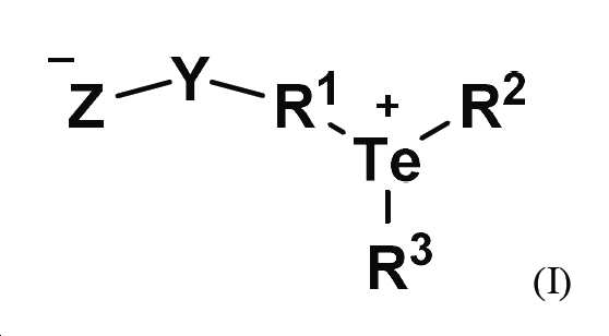
- 제1항에 있어서, 하기 화학식 (I)에 상응하는 것인 쯔비터이온:

식 중, R1, R2 및 R3는 각각 동일한 또는 상이한 비-수소 치환기이고, R1, R2 및 R3 중 2개 이상이 임의로 함께 취해져 고리를 형성할 수 있고;
Y는 부재이거나 또는 링커기이고;
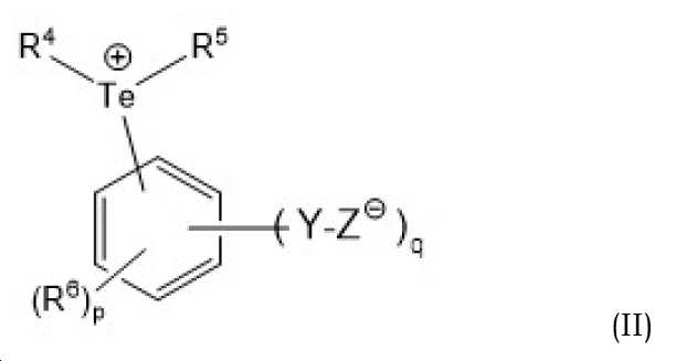
Z는 음이온성기이다. - 제1항에 있어서, 하기 화학식 (II)에 상응하는 것인 쯔비터이온:

여기서 화학식 (II)에서,
R4, R5 및 각각의 R6는 동일한 또는 상이한 비-수소 치환기이고;
p는 0 내지 5의 정수이고;
Y는 부재이거나 또는 링커기이고;
Z는 음이온성기이고;
q는 0 또는 1이고, p와 q의 합은 5를 초과하지 않으며, q가 0인 경우, 이때 R4 및/또는 R5는 음이온성기를 포함한다. - 제3항에 있어서, R4 및/또는 R5가 음이온성기를 포함하는 쯔비터이온.
- 제1항에 있어서, 하기 화학식 (III)에 상응하는 것인 쯔비터이온:

식 중,
X는 단일 결합 또는 도시된 Te 원자와 함께 단일 고리기 또는 다중 융합된 또는 연결된 고리 구조를 형성하는 연결기이고;
R7은 비-수소 치환기이고;
각각의 R7'은 동일한 또는 상이한 비-수소 고리 치환기이고;
Y는 부재이거나 또는 링커기이고;
Z는 음이온성기이고;
p는 0 (여기서 R7'기는 존재하지 않음) 내지 고리원에 의해 허용되는 최대 원자가의 정수이고;
q는 0 또는 양의 정수이고, q가 0인 경우, 이때 R7은 음이온성기를 포함한다. - 제5항에 있어서, R7은 음이온성기를 포함하는 쯔비터이온.
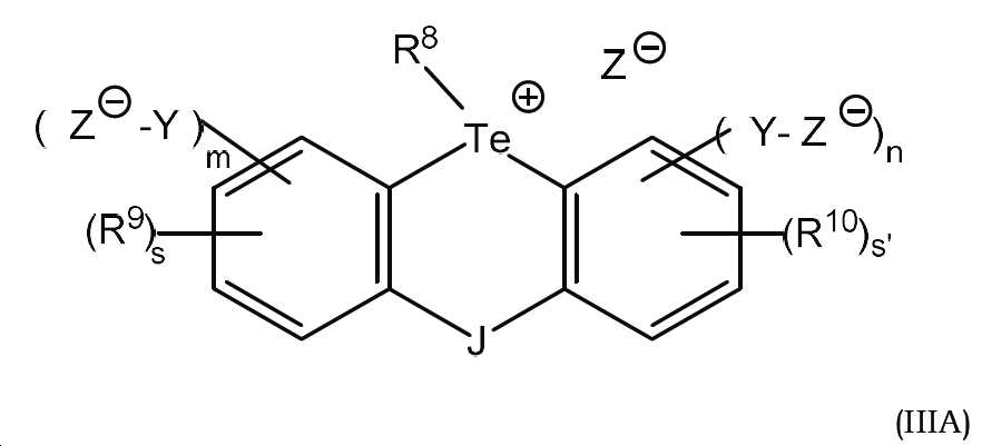
- 제1항에 있어서, 하기 화학식 (IIIA)에 상응하는 것인 쯔비터이온:

식 중,
R8는 비-수소 치환기이고;
R9 및 R10은 동일한 또는 상이한 비-수소 고리 치환기이고;
J는 단일 결합 또는 연결기이고;
s 및 s'는 각각 독립적으로 0, 1, 2, 3, 및 4의 정수이고;
Y는 부재이거나 또는 링커기이고;
Z는 음이온성기이고;
각각의 m 및 n은 0 또는 1이고, m과 n의 합은 1을 초과하지 않고; 각각의 m 및 n이 0인 경우, 이때 R8는 음이온성기를 포함한다. - 제7항에 있어서, 상기 R8은 음이온성기를 포함하는 쯔비터이온.
- 제1항 내지 제8항 중 어느 한 항에 있어서, 중합성기 및/또는 하나 이상의 산 분해성 기를 포함하는 쯔비터이온.
- 수지 및 제1항 내지 제9항 중 어느 한 항의 하나 이상의 쯔비터이온을 포함하는 포토레지스트 조성물.
- 제10항에 있어서, 상기 하나 이상의 쯔비터이온과 구별되는 하나 이상의 산 발생제 화합물을 포함하는 포토레지스트 조성물.
- 포토레지스트 릴리프 이미지를 제공하는 방법으로서,
a) 제10항 또는 제11항의 포토레지스트의 코팅층을 기판 상에 도포하는 단계; 및
b) 포토레지스트 조성물층을 활성화 방사선에 노광시키고, 노광된 포토레지스트 조성물 코팅층을 현상시키는 단계
를 포함하는 포토레지스트 릴리프 이미지를 제공하는 방법.
Applications Claiming Priority (2)
| Application Number | Priority Date | Filing Date | Title |
|---|---|---|---|
| US201762593240P | 2017-11-30 | 2017-11-30 | |
| US62/593,240 | 2017-11-30 |
Publications (2)
| Publication Number | Publication Date |
|---|---|
| KR20190064458A true KR20190064458A (ko) | 2019-06-10 |
| KR102163904B1 KR102163904B1 (ko) | 2020-10-12 |
Family
ID=66634302
Family Applications (1)
| Application Number | Title | Priority Date | Filing Date |
|---|---|---|---|
| KR1020180147074A Active KR102163904B1 (ko) | 2017-11-30 | 2018-11-26 | 쯔비터이온 화합물 및 이를 포함하는 포토레지스트 |
Country Status (5)
| Country | Link |
|---|---|
| US (1) | US11505565B2 (ko) |
| JP (1) | JP6810728B2 (ko) |
| KR (1) | KR102163904B1 (ko) |
| CN (2) | CN109928904A (ko) |
| TW (1) | TWI683801B (ko) |
Families Citing this family (2)
| Publication number | Priority date | Publication date | Assignee | Title |
|---|---|---|---|---|
| CN109851539A (zh) * | 2017-11-30 | 2019-06-07 | 罗门哈斯电子材料有限责任公司 | 盐和包含其的光致抗蚀剂 |
| TWI733069B (zh) * | 2017-12-31 | 2021-07-11 | 美商羅門哈斯電子材料有限公司 | 單體、聚合物及包含其的微影組合物 |
Citations (4)
| Publication number | Priority date | Publication date | Assignee | Title |
|---|---|---|---|---|
| JP2001174983A (ja) * | 1999-11-12 | 2001-06-29 | Hyundai Electronics Ind Co Ltd | Tips工程用フォトレジスト組成物 |
| US20110084321A1 (en) * | 2005-07-29 | 2011-04-14 | Semiconductor Energy Laboratory Co., Ltd. | Semiconductor device and manufacturing method thereof |
| JP2014170205A (ja) * | 2013-02-08 | 2014-09-18 | Fujifilm Corp | パターン形成方法、それに用いられる感活性光線性又は感放射線性樹脂組成物、及び、レジスト膜、並びに、これらを用いる電子デバイスの製造方法、及び、電子デバイス |
| US20190155152A1 (en) * | 2017-11-20 | 2019-05-23 | Rohm And Haas Electronic Materials Llc | Iodine-containing photoacid generators and compositions comprising the same |
Family Cites Families (37)
| Publication number | Priority date | Publication date | Assignee | Title |
|---|---|---|---|---|
| CA1087900A (en) | 1977-04-01 | 1980-10-21 | Mark Lelental | Electrically activated recording material containing a te(ii) coordination complex |
| US4258128A (en) * | 1978-12-01 | 1981-03-24 | Eastman Kodak Company | Tellurium(II) compounds and complexes having organic moieties containing silicon containing compositions, articles and photoimaging processes |
| US5212046A (en) | 1989-10-17 | 1993-05-18 | Shipley Company Inc. | Near UV photoresist |
| US5164524A (en) | 1990-02-06 | 1992-11-17 | The United States Of America As Represented By The Secretary Of The Navy | Process for preparing tetra (organyl) telluride compounds |
| JPH07146528A (ja) | 1993-11-24 | 1995-06-06 | Konica Corp | 画像形成組成物、画像形成材料及び画像形成方法 |
| US5879856A (en) | 1995-12-05 | 1999-03-09 | Shipley Company, L.L.C. | Chemically amplified positive photoresists |
| US6090526A (en) | 1996-09-13 | 2000-07-18 | Shipley Company, L.L.C. | Polymers and photoresist compositions |
| TW470785B (en) * | 1998-02-03 | 2002-01-01 | Atotech Deutschland Gmbh | Process for preliminary treatment of copper surfaces |
| JP2001075284A (ja) | 1998-12-03 | 2001-03-23 | Fuji Photo Film Co Ltd | ポジ型レジスト組成物 |
| JP2001255647A (ja) | 2000-03-13 | 2001-09-21 | Daikin Ind Ltd | エネルギー線照射によりカチオンまたは酸を発生するフルオロアルキルオニウム塩型のカチオンまたは酸発生剤 |
| US7326514B2 (en) | 2003-03-12 | 2008-02-05 | Cornell Research Foundation, Inc. | Organoelement resists for EUV lithography and methods of making the same |
| US7122294B2 (en) | 2003-05-22 | 2006-10-17 | 3M Innovative Properties Company | Photoacid generators with perfluorinated multifunctional anions |
| JP2005128049A (ja) | 2003-10-21 | 2005-05-19 | Jsr Corp | 感放射線性樹脂組成物 |
| US20060115768A1 (en) | 2004-11-30 | 2006-06-01 | Fuji Photo Film Co. Ltd | Lithographic printing plate precursor, plate-making method, and lithographic printing method |
| US8039194B2 (en) | 2008-01-08 | 2011-10-18 | Internatinal Business Machines Corporation | Photoacid generators for extreme ultraviolet lithography |
| JP5387181B2 (ja) * | 2009-07-08 | 2014-01-15 | 信越化学工業株式会社 | スルホニウム塩、レジスト材料及びパターン形成方法 |
| JP5782283B2 (ja) * | 2010-03-31 | 2015-09-24 | ローム アンド ハース エレクトロニック マテリアルズ エルエルシーRohm and Haas Electronic Materials LLC | 新規のポリマーおよびフォトレジスト組成物 |
| IL213195A0 (en) | 2010-05-31 | 2011-07-31 | Rohm & Haas Elect Mat | Photoresist compositions and emthods of forming photolithographic patterns |
| EP2472322A2 (en) | 2010-12-31 | 2012-07-04 | Rohm and Haas Electronic Materials LLC | Photoacid generating monomer and precursor thereof |
| JP2013008020A (ja) * | 2011-05-25 | 2013-01-10 | Sumitomo Chemical Co Ltd | レジスト組成物 |
| KR101830780B1 (ko) | 2011-08-05 | 2018-04-05 | 삼성전자주식회사 | 박막의 제조방법, 박막, 박막의 제조장치 및 전자소자 |
| JP5723802B2 (ja) * | 2012-02-16 | 2015-05-27 | 富士フイルム株式会社 | 感活性光線性又は感放射線性樹脂組成物、及び該組成物を用いたパターン形成方法及びレジスト膜、並びにこれらを用いた電子デバイスの製造方法 |
| JP6155013B2 (ja) * | 2012-11-19 | 2017-06-28 | 東京応化工業株式会社 | レジスト組成物及びレジストパターン形成方法 |
| US9063420B2 (en) | 2013-07-16 | 2015-06-23 | Rohm And Haas Electronic Materials Llc | Photoresist composition, coated substrate, and method of forming electronic device |
| US9372402B2 (en) * | 2013-09-13 | 2016-06-21 | The Research Foundation For The State University Of New York | Molecular organometallic resists for EUV |
| WO2015046021A1 (ja) * | 2013-09-26 | 2015-04-02 | Jsr株式会社 | 感放射線性樹脂組成物及びレジストパターン形成方法 |
| US9229319B2 (en) | 2013-12-19 | 2016-01-05 | Rohm And Haas Electronic Materials Llc | Photoacid-generating copolymer and associated photoresist composition, coated substrate, and method of forming an electronic device |
| JP6125468B2 (ja) * | 2014-07-04 | 2017-05-10 | 信越化学工業株式会社 | 光酸発生剤、化学増幅型レジスト材料及びパターン形成方法 |
| EP3343290A4 (en) | 2015-08-24 | 2019-09-04 | A School Corporation Kansai University | LITHOGRAPHIC MATERIAL AND METHOD OF MANUFACTURING THEREOF, LITHOGRAPHIC COMPOSITION, PATTERN PROCESSING, COMPOUND, RESIN AND METHOD OF PROCESSING FOR CONNECTION AND RESIN |
| KR20190003528A (ko) | 2016-04-28 | 2019-01-09 | 미쯔비시 가스 케미칼 컴파니, 인코포레이티드 | 레지스트 하층막 형성용 조성물, 리소그래피용 하층막, 및, 패턴 형성방법 |
| JP2019113571A (ja) | 2016-04-28 | 2019-07-11 | 三菱瓦斯化学株式会社 | レジスト下層膜形成用組成物、並びに、それを用いたリソグラフィー用下層膜及びパターン形成方法 |
| WO2018117167A1 (ja) | 2016-12-21 | 2018-06-28 | 東洋合成工業株式会社 | 感光性化合物、該感光性化合物を含有する光酸発生剤及びレジスト組成物、並びに、該レジスト組成物を用いたデバイスの製造方法 |
| JP6820233B2 (ja) | 2017-05-26 | 2021-01-27 | 東洋合成工業株式会社 | ポリマー、該ポリマーを含有するレジスト組成物及びそれを用いたデバイスの製造方法 |
| CN109856911B (zh) | 2017-11-30 | 2023-10-27 | 罗门哈斯电子材料有限责任公司 | 盐和包含其的光致抗蚀剂 |
| CN109851539A (zh) | 2017-11-30 | 2019-06-07 | 罗门哈斯电子材料有限责任公司 | 盐和包含其的光致抗蚀剂 |
| TWI733069B (zh) | 2017-12-31 | 2021-07-11 | 美商羅門哈斯電子材料有限公司 | 單體、聚合物及包含其的微影組合物 |
| CN112088336A (zh) | 2018-04-27 | 2020-12-15 | 三菱瓦斯化学株式会社 | 抗蚀剂下层膜形成用组合物和图案形成方法 |
-
2018
- 2018-11-22 JP JP2018219756A patent/JP6810728B2/ja active Active
- 2018-11-22 TW TW107141626A patent/TWI683801B/zh active
- 2018-11-22 CN CN201811397335.6A patent/CN109928904A/zh active Pending
- 2018-11-22 CN CN202411181742.9A patent/CN119080661A/zh active Pending
- 2018-11-26 KR KR1020180147074A patent/KR102163904B1/ko active Active
- 2018-11-29 US US16/204,960 patent/US11505565B2/en active Active
Patent Citations (4)
| Publication number | Priority date | Publication date | Assignee | Title |
|---|---|---|---|---|
| JP2001174983A (ja) * | 1999-11-12 | 2001-06-29 | Hyundai Electronics Ind Co Ltd | Tips工程用フォトレジスト組成物 |
| US20110084321A1 (en) * | 2005-07-29 | 2011-04-14 | Semiconductor Energy Laboratory Co., Ltd. | Semiconductor device and manufacturing method thereof |
| JP2014170205A (ja) * | 2013-02-08 | 2014-09-18 | Fujifilm Corp | パターン形成方法、それに用いられる感活性光線性又は感放射線性樹脂組成物、及び、レジスト膜、並びに、これらを用いる電子デバイスの製造方法、及び、電子デバイス |
| US20190155152A1 (en) * | 2017-11-20 | 2019-05-23 | Rohm And Haas Electronic Materials Llc | Iodine-containing photoacid generators and compositions comprising the same |
Non-Patent Citations (1)
| Title |
|---|
| Journal of Organometallic Chemistry, 832(2017), pp.66~71(2017.01.25. 공개) 1부.* * |
Also Published As
| Publication number | Publication date |
|---|---|
| JP6810728B2 (ja) | 2021-01-06 |
| TW201925171A (zh) | 2019-07-01 |
| US11505565B2 (en) | 2022-11-22 |
| TWI683801B (zh) | 2020-02-01 |
| CN109928904A (zh) | 2019-06-25 |
| JP2019099558A (ja) | 2019-06-24 |
| CN119080661A (zh) | 2024-12-06 |
| KR102163904B1 (ko) | 2020-10-12 |
| US20190161509A1 (en) | 2019-05-30 |
Similar Documents
| Publication | Publication Date | Title |
|---|---|---|
| TWI733069B (zh) | 單體、聚合物及包含其的微影組合物 | |
| KR102204530B1 (ko) | 산 발생제 및 이를 포함하는 포토레지스트 | |
| KR102394708B1 (ko) | 산 발생제 화합물 및 이를 포함하는 포토레지스트 | |
| US11448960B2 (en) | Salts and photoresists comprising same | |
| KR102319656B1 (ko) | 아릴 아세테이트 오늄 물질 | |
| JP7357034B2 (ja) | 塩およびこれを含むフォトレジスト | |
| KR102163904B1 (ko) | 쯔비터이온 화합물 및 이를 포함하는 포토레지스트 |
Legal Events
| Date | Code | Title | Description |
|---|---|---|---|
| A201 | Request for examination | ||
| E13-X000 | Pre-grant limitation requested |
St.27 status event code: A-2-3-E10-E13-lim-X000 |
|
| PA0109 | Patent application |
St.27 status event code: A-0-1-A10-A12-nap-PA0109 |
|
| PA0201 | Request for examination |
St.27 status event code: A-1-2-D10-D11-exm-PA0201 |
|
| R17-X000 | Change to representative recorded |
St.27 status event code: A-3-3-R10-R17-oth-X000 |
|
| D13-X000 | Search requested |
St.27 status event code: A-1-2-D10-D13-srh-X000 |
|
| PG1501 | Laying open of application |
St.27 status event code: A-1-1-Q10-Q12-nap-PG1501 |
|
| D14-X000 | Search report completed |
St.27 status event code: A-1-2-D10-D14-srh-X000 |
|
| E902 | Notification of reason for refusal | ||
| PE0902 | Notice of grounds for rejection |
St.27 status event code: A-1-2-D10-D21-exm-PE0902 |
|
| AMND | Amendment | ||
| P11-X000 | Amendment of application requested |
St.27 status event code: A-2-2-P10-P11-nap-X000 |
|
| P13-X000 | Application amended |
St.27 status event code: A-2-2-P10-P13-nap-X000 |
|
| E601 | Decision to refuse application | ||
| PE0601 | Decision on rejection of patent |
St.27 status event code: N-2-6-B10-B15-exm-PE0601 |
|
| X091 | Application refused [patent] | ||
| AMND | Amendment | ||
| E13-X000 | Pre-grant limitation requested |
St.27 status event code: A-2-3-E10-E13-lim-X000 |
|
| P11-X000 | Amendment of application requested |
St.27 status event code: A-2-2-P10-P11-nap-X000 |
|
| P13-X000 | Application amended |
St.27 status event code: A-2-2-P10-P13-nap-X000 |
|
| PX0901 | Re-examination |
St.27 status event code: A-2-3-E10-E12-rex-PX0901 |
|
| PX0701 | Decision of registration after re-examination |
St.27 status event code: A-3-4-F10-F13-rex-PX0701 |
|
| X701 | Decision to grant (after re-examination) | ||
| GRNT | Written decision to grant | ||
| PR0701 | Registration of establishment |
St.27 status event code: A-2-4-F10-F11-exm-PR0701 |
|
| PR1002 | Payment of registration fee |
St.27 status event code: A-2-2-U10-U11-oth-PR1002 Fee payment year number: 1 |
|
| PG1601 | Publication of registration |
St.27 status event code: A-4-4-Q10-Q13-nap-PG1601 |
|
| PR1001 | Payment of annual fee |
St.27 status event code: A-4-4-U10-U11-oth-PR1001 Fee payment year number: 4 |
|
| PN2301 | Change of applicant |
St.27 status event code: A-5-5-R10-R13-asn-PN2301 St.27 status event code: A-5-5-R10-R11-asn-PN2301 |
|
| PR1001 | Payment of annual fee |
St.27 status event code: A-4-4-U10-U11-oth-PR1001 Fee payment year number: 5 |
|
| P22-X000 | Classification modified |
St.27 status event code: A-4-4-P10-P22-nap-X000 |