KR20190133112A - 기판 처리 장치 - Google Patents
기판 처리 장치 Download PDFInfo
- Publication number
- KR20190133112A KR20190133112A KR1020190059587A KR20190059587A KR20190133112A KR 20190133112 A KR20190133112 A KR 20190133112A KR 1020190059587 A KR1020190059587 A KR 1020190059587A KR 20190059587 A KR20190059587 A KR 20190059587A KR 20190133112 A KR20190133112 A KR 20190133112A
- Authority
- KR
- South Korea
- Prior art keywords
- light source
- chamber
- substrate
- gas supply
- processing
- Prior art date
- Legal status (The legal status is an assumption and is not a legal conclusion. Google has not performed a legal analysis and makes no representation as to the accuracy of the status listed.)
- Granted
Links
Images





Classifications
-
- H01L21/67017—
-
- H—ELECTRICITY
- H10—SEMICONDUCTOR DEVICES; ELECTRIC SOLID-STATE DEVICES NOT OTHERWISE PROVIDED FOR
- H10P—GENERIC PROCESSES OR APPARATUS FOR THE MANUFACTURE OR TREATMENT OF DEVICES COVERED BY CLASS H10
- H10P72/00—Handling or holding of wafers, substrates or devices during manufacture or treatment thereof
- H10P72/04—Apparatus for manufacture or treatment
- H10P72/0402—Apparatus for fluid treatment
-
- G—PHYSICS
- G03—PHOTOGRAPHY; CINEMATOGRAPHY; ANALOGOUS TECHNIQUES USING WAVES OTHER THAN OPTICAL WAVES; ELECTROGRAPHY; HOLOGRAPHY
- G03F—PHOTOMECHANICAL PRODUCTION OF TEXTURED OR PATTERNED SURFACES, e.g. FOR PRINTING, FOR PROCESSING OF SEMICONDUCTOR DEVICES; MATERIALS THEREFOR; ORIGINALS THEREFOR; APPARATUS SPECIALLY ADAPTED THEREFOR
- G03F7/00—Photomechanical, e.g. photolithographic, production of textured or patterned surfaces, e.g. printing surfaces; Materials therefor, e.g. comprising photoresists; Apparatus specially adapted therefor
- G03F7/26—Processing photosensitive materials; Apparatus therefor
- G03F7/40—Treatment after imagewise removal, e.g. baking
-
- G—PHYSICS
- G03—PHOTOGRAPHY; CINEMATOGRAPHY; ANALOGOUS TECHNIQUES USING WAVES OTHER THAN OPTICAL WAVES; ELECTROGRAPHY; HOLOGRAPHY
- G03F—PHOTOMECHANICAL PRODUCTION OF TEXTURED OR PATTERNED SURFACES, e.g. FOR PRINTING, FOR PROCESSING OF SEMICONDUCTOR DEVICES; MATERIALS THEREFOR; ORIGINALS THEREFOR; APPARATUS SPECIALLY ADAPTED THEREFOR
- G03F7/00—Photomechanical, e.g. photolithographic, production of textured or patterned surfaces, e.g. printing surfaces; Materials therefor, e.g. comprising photoresists; Apparatus specially adapted therefor
- G03F7/20—Exposure; Apparatus therefor
- G03F7/2002—Exposure; Apparatus therefor with visible light or UV light, through an original having an opaque pattern on a transparent support, e.g. film printing, projection printing; by reflection of visible or UV light from an original such as a printed image
-
- G—PHYSICS
- G03—PHOTOGRAPHY; CINEMATOGRAPHY; ANALOGOUS TECHNIQUES USING WAVES OTHER THAN OPTICAL WAVES; ELECTROGRAPHY; HOLOGRAPHY
- G03F—PHOTOMECHANICAL PRODUCTION OF TEXTURED OR PATTERNED SURFACES, e.g. FOR PRINTING, FOR PROCESSING OF SEMICONDUCTOR DEVICES; MATERIALS THEREFOR; ORIGINALS THEREFOR; APPARATUS SPECIALLY ADAPTED THEREFOR
- G03F7/00—Photomechanical, e.g. photolithographic, production of textured or patterned surfaces, e.g. printing surfaces; Materials therefor, e.g. comprising photoresists; Apparatus specially adapted therefor
- G03F7/20—Exposure; Apparatus therefor
- G03F7/2002—Exposure; Apparatus therefor with visible light or UV light, through an original having an opaque pattern on a transparent support, e.g. film printing, projection printing; by reflection of visible or UV light from an original such as a printed image
- G03F7/2004—Exposure; Apparatus therefor with visible light or UV light, through an original having an opaque pattern on a transparent support, e.g. film printing, projection printing; by reflection of visible or UV light from an original such as a printed image characterised by the use of a particular light source, e.g. fluorescent lamps or deep UV light
-
- G—PHYSICS
- G03—PHOTOGRAPHY; CINEMATOGRAPHY; ANALOGOUS TECHNIQUES USING WAVES OTHER THAN OPTICAL WAVES; ELECTROGRAPHY; HOLOGRAPHY
- G03F—PHOTOMECHANICAL PRODUCTION OF TEXTURED OR PATTERNED SURFACES, e.g. FOR PRINTING, FOR PROCESSING OF SEMICONDUCTOR DEVICES; MATERIALS THEREFOR; ORIGINALS THEREFOR; APPARATUS SPECIALLY ADAPTED THEREFOR
- G03F7/00—Photomechanical, e.g. photolithographic, production of textured or patterned surfaces, e.g. printing surfaces; Materials therefor, e.g. comprising photoresists; Apparatus specially adapted therefor
- G03F7/20—Exposure; Apparatus therefor
- G03F7/2022—Multi-step exposure, e.g. hybrid; backside exposure; blanket exposure, e.g. for image reversal; edge exposure, e.g. for edge bead removal; corrective exposure
-
- G—PHYSICS
- G03—PHOTOGRAPHY; CINEMATOGRAPHY; ANALOGOUS TECHNIQUES USING WAVES OTHER THAN OPTICAL WAVES; ELECTROGRAPHY; HOLOGRAPHY
- G03F—PHOTOMECHANICAL PRODUCTION OF TEXTURED OR PATTERNED SURFACES, e.g. FOR PRINTING, FOR PROCESSING OF SEMICONDUCTOR DEVICES; MATERIALS THEREFOR; ORIGINALS THEREFOR; APPARATUS SPECIALLY ADAPTED THEREFOR
- G03F7/00—Photomechanical, e.g. photolithographic, production of textured or patterned surfaces, e.g. printing surfaces; Materials therefor, e.g. comprising photoresists; Apparatus specially adapted therefor
- G03F7/20—Exposure; Apparatus therefor
- G03F7/2022—Multi-step exposure, e.g. hybrid; backside exposure; blanket exposure, e.g. for image reversal; edge exposure, e.g. for edge bead removal; corrective exposure
- G03F7/2024—Multi-step exposure, e.g. hybrid; backside exposure; blanket exposure, e.g. for image reversal; edge exposure, e.g. for edge bead removal; corrective exposure of the already developed image
-
- G—PHYSICS
- G03—PHOTOGRAPHY; CINEMATOGRAPHY; ANALOGOUS TECHNIQUES USING WAVES OTHER THAN OPTICAL WAVES; ELECTROGRAPHY; HOLOGRAPHY
- G03F—PHOTOMECHANICAL PRODUCTION OF TEXTURED OR PATTERNED SURFACES, e.g. FOR PRINTING, FOR PROCESSING OF SEMICONDUCTOR DEVICES; MATERIALS THEREFOR; ORIGINALS THEREFOR; APPARATUS SPECIALLY ADAPTED THEREFOR
- G03F7/00—Photomechanical, e.g. photolithographic, production of textured or patterned surfaces, e.g. printing surfaces; Materials therefor, e.g. comprising photoresists; Apparatus specially adapted therefor
- G03F7/70—Microphotolithographic exposure; Apparatus therefor
- G03F7/70008—Production of exposure light, i.e. light sources
- G03F7/70033—Production of exposure light, i.e. light sources by plasma extreme ultraviolet [EUV] sources
-
- G—PHYSICS
- G03—PHOTOGRAPHY; CINEMATOGRAPHY; ANALOGOUS TECHNIQUES USING WAVES OTHER THAN OPTICAL WAVES; ELECTROGRAPHY; HOLOGRAPHY
- G03F—PHOTOMECHANICAL PRODUCTION OF TEXTURED OR PATTERNED SURFACES, e.g. FOR PRINTING, FOR PROCESSING OF SEMICONDUCTOR DEVICES; MATERIALS THEREFOR; ORIGINALS THEREFOR; APPARATUS SPECIALLY ADAPTED THEREFOR
- G03F7/00—Photomechanical, e.g. photolithographic, production of textured or patterned surfaces, e.g. printing surfaces; Materials therefor, e.g. comprising photoresists; Apparatus specially adapted therefor
- G03F7/70—Microphotolithographic exposure; Apparatus therefor
- G03F7/708—Construction of apparatus, e.g. environment aspects, hygiene aspects or materials
- G03F7/70908—Hygiene, e.g. preventing apparatus pollution, mitigating effect of pollution or removing pollutants from apparatus
-
- G—PHYSICS
- G03—PHOTOGRAPHY; CINEMATOGRAPHY; ANALOGOUS TECHNIQUES USING WAVES OTHER THAN OPTICAL WAVES; ELECTROGRAPHY; HOLOGRAPHY
- G03F—PHOTOMECHANICAL PRODUCTION OF TEXTURED OR PATTERNED SURFACES, e.g. FOR PRINTING, FOR PROCESSING OF SEMICONDUCTOR DEVICES; MATERIALS THEREFOR; ORIGINALS THEREFOR; APPARATUS SPECIALLY ADAPTED THEREFOR
- G03F7/00—Photomechanical, e.g. photolithographic, production of textured or patterned surfaces, e.g. printing surfaces; Materials therefor, e.g. comprising photoresists; Apparatus specially adapted therefor
- G03F7/70—Microphotolithographic exposure; Apparatus therefor
- G03F7/708—Construction of apparatus, e.g. environment aspects, hygiene aspects or materials
- G03F7/70908—Hygiene, e.g. preventing apparatus pollution, mitigating effect of pollution or removing pollutants from apparatus
- G03F7/70933—Purge, e.g. exchanging fluid or gas to remove pollutants
-
- H01L21/027—
-
- H01L21/67253—
-
- H01L21/67276—
-
- H—ELECTRICITY
- H10—SEMICONDUCTOR DEVICES; ELECTRIC SOLID-STATE DEVICES NOT OTHERWISE PROVIDED FOR
- H10P—GENERIC PROCESSES OR APPARATUS FOR THE MANUFACTURE OR TREATMENT OF DEVICES COVERED BY CLASS H10
- H10P72/00—Handling or holding of wafers, substrates or devices during manufacture or treatment thereof
- H10P72/06—Apparatus for monitoring, sorting, marking, testing or measuring
- H10P72/0604—Process monitoring, e.g. flow or thickness monitoring
-
- H—ELECTRICITY
- H10—SEMICONDUCTOR DEVICES; ELECTRIC SOLID-STATE DEVICES NOT OTHERWISE PROVIDED FOR
- H10P—GENERIC PROCESSES OR APPARATUS FOR THE MANUFACTURE OR TREATMENT OF DEVICES COVERED BY CLASS H10
- H10P72/00—Handling or holding of wafers, substrates or devices during manufacture or treatment thereof
- H10P72/06—Apparatus for monitoring, sorting, marking, testing or measuring
- H10P72/0612—Production flow monitoring, e.g. for increasing throughput
-
- H—ELECTRICITY
- H10—SEMICONDUCTOR DEVICES; ELECTRIC SOLID-STATE DEVICES NOT OTHERWISE PROVIDED FOR
- H10P—GENERIC PROCESSES OR APPARATUS FOR THE MANUFACTURE OR TREATMENT OF DEVICES COVERED BY CLASS H10
- H10P76/00—Manufacture or treatment of masks on semiconductor bodies, e.g. by lithography or photolithography
-
- H—ELECTRICITY
- H10—SEMICONDUCTOR DEVICES; ELECTRIC SOLID-STATE DEVICES NOT OTHERWISE PROVIDED FOR
- H10P—GENERIC PROCESSES OR APPARATUS FOR THE MANUFACTURE OR TREATMENT OF DEVICES COVERED BY CLASS H10
- H10P76/00—Manufacture or treatment of masks on semiconductor bodies, e.g. by lithography or photolithography
- H10P76/20—Manufacture or treatment of masks on semiconductor bodies, e.g. by lithography or photolithography of masks comprising organic materials
- H10P76/204—Manufacture or treatment of masks on semiconductor bodies, e.g. by lithography or photolithography of masks comprising organic materials of organic photoresist masks
Landscapes
- Physics & Mathematics (AREA)
- General Physics & Mathematics (AREA)
- Public Health (AREA)
- Health & Medical Sciences (AREA)
- Epidemiology (AREA)
- Engineering & Computer Science (AREA)
- Environmental & Geological Engineering (AREA)
- Atmospheric Sciences (AREA)
- Life Sciences & Earth Sciences (AREA)
- Plasma & Fusion (AREA)
- Drying Of Semiconductors (AREA)
- Exposure Of Semiconductors, Excluding Electron Or Ion Beam Exposure (AREA)
- Automation & Control Theory (AREA)
- Container, Conveyance, Adherence, Positioning, Of Wafer (AREA)
- Cleaning Or Drying Semiconductors (AREA)
- Photosensitive Polymer And Photoresist Processing (AREA)
- Exposure And Positioning Against Photoresist Photosensitive Materials (AREA)
- Manufacturing Of Printed Wiring (AREA)
- Electrical Discharge Machining, Electrochemical Machining, And Combined Machining (AREA)
Abstract
기판 처리 장치는, 기판의 처리가 행해지도록 구성된 처리실과, 기판의 표면에 진공 자외광을 조사하도록 구성된 광원을 포함하는 광원실과, 광원실 내에 불활성 가스를 공급하도록 구성된 가스 공급부와, 광원실 내를 불활성 가스 분위기로 유지하도록 가스 공급부를 제어하는 처리를 실행하는 제어부를 구비한다.
Description
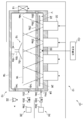
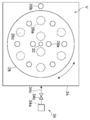
도 2는 도 1의 기판 처리 장치의 램프실 내를 상방에서 본 도면이고, 광 통과창이 셔터 부재에 의해 폐쇄되어 있지 않은 상태를 도시한 도면이다.
도 3은 도 1의 기판 처리 장치의 램프실 내를 상방에서 본 도면이고, 광 통과창이 셔터 부재에 의해 폐쇄된 상태를 도시한 도면이다.
도 4는 기판 처리 장치를 도시한 블록도이다.
도 5는 컨트롤러의 하드웨어 구성을 도시한 개략도이다.
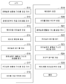
도 6은 웨이퍼의 처리 순서의 일례를 도시한 흐름도이다.
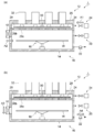
도 7은 웨이퍼의 처리 순서의 일례를 설명하기 위한 도면이다.
도 8은 웨이퍼의 처리 순서의 일례를 설명하기 위한 도면이다.
도 9는 웨이퍼의 처리 순서의 일례를 설명하기 위한 도면이다.
도 10은 처리실 내의 압력이 처리의 진행에 따라 변화하는 모습을 설명하기 위한 도면이다.
도 11은 다른 예에 따른 기판 처리 장치의 램프실 내를 상방에서 본 도면이다.
도 12는 다른 예에 따른 기판 처리 장치의 램프실 내를 상방에서 본 도면이다.
Claims (8)
- 기판 처리 장치에 있어서,
기판의 처리가 행해지도록 구성된 처리실과,
상기 기판의 표면에 진공 자외광을 조사하도록 구성된 광원을 포함하는 광원실과,
상기 광원실 내에 불활성 가스를 공급하도록 구성된 가스 공급부와,
상기 광원실 내를 불활성 가스 분위기로 유지하도록 상기 가스 공급부를 제어하는 처리를 실행하는 제어부
를 포함하는, 기판 처리 장치. - 제1항에 있어서, 상기 처리실과 상기 광원실 사이를 유체적으로 접속하는 유로를 더 포함하는, 기판 처리 장치.
- 제2항에 있어서,
상기 처리실로부터 기체를 배기하도록 구성된 배기부를 더 포함하고,
상기 가스 공급부를 제어하는 처리는, 적어도 상기 배기부가 정지하고 있을 때에, 상기 광원실 내에 불활성 가스를 공급하도록 상기 가스 공급부 및 상기 배기부를 제어하는 처리를 포함하는 것인, 기판 처리 장치. - 제2항 또는 제3항에 있어서,
상기 가스 공급부를 제어하는 처리는, 상기 광원실 내에 불활성 가스가 공급되고 있을 때에, 상기 처리실 내의 압력보다 상기 광원실 내의 압력이 높아지도록 상기 가스 공급부를 제어하는 처리를 포함하는 것인, 기판 처리 장치. - 제1항 내지 제4항 중 어느 한 항에 있어서,
상기 가스 공급부를 제어하는 처리는, 적어도 상기 처리실이 대기 개방되어 있을 때에, 상기 광원실 내에 불활성 가스를 공급하도록 상기 가스 공급부를 제어하는 처리를 포함하는 것인, 기판 처리 장치. - 제1항 내지 제5항 중 어느 한 항에 있어서,
상기 가스 공급부를 제어하는 처리는, 상기 광원실 내 및 상기 처리실 내에 각각 불활성 가스를 공급하도록 상기 가스 공급부를 제어하는 처리를 포함하는 것인, 기판 처리 장치. - 제1항 내지 제6항 중 어느 한 항에 있어서,
상기 광원실은, 상기 광원과 상기 기판 사이에 위치하도록 상기 광원실 내에 배치된 셔터 부재를 포함하고,
상기 셔터 부재는, 상기 광원으로부터의 진공 자외광을 상기 기판에 도달시키지 않는 폐쇄 위치와, 상기 광원으로부터의 진공 자외광을 상기 기판에 통과시키는 개방 위치 사이에서 이동 가능하게 구성되어 있으며,
상기 제어부는, 처리실 내의 산소 농도가 목표값 이하가 되었을 때에 상기 셔터 부재를 상기 개방 위치로 하도록 상기 셔터 부재를 제어하는 처리를 실행하는 것인, 기판 처리 장치. - 제1항 내지 제7항 중 어느 한 항에 있어서,
상기 광원실 내의 공간은, 상기 기판의 상기 표면에 직교하는 방향에 있어서의 높이가 상대적으로 작은 편평 공간을 나타내고 있고,
상기 가스 공급부에 의해 상기 광원실 내에 공급되는 불활성 가스는, 상기 기판의 상기 표면을 따르는 방향으로 흐르는 것인, 기판 처리 장치.
Applications Claiming Priority (2)
| Application Number | Priority Date | Filing Date | Title |
|---|---|---|---|
| JP2018097663A JP7058177B2 (ja) | 2018-05-22 | 2018-05-22 | 基板処理装置 |
| JPJP-P-2018-097663 | 2018-05-22 |
Publications (2)
| Publication Number | Publication Date |
|---|---|
| KR20190133112A true KR20190133112A (ko) | 2019-12-02 |
| KR102688406B1 KR102688406B1 (ko) | 2024-07-24 |
Family
ID=68614499
Family Applications (1)
| Application Number | Title | Priority Date | Filing Date |
|---|---|---|---|
| KR1020190059587A Active KR102688406B1 (ko) | 2018-05-22 | 2019-05-21 | 기판 처리 장치 |
Country Status (5)
| Country | Link |
|---|---|
| US (1) | US11353792B2 (ko) |
| JP (1) | JP7058177B2 (ko) |
| KR (1) | KR102688406B1 (ko) |
| CN (1) | CN110517952B (ko) |
| TW (1) | TWI821289B (ko) |
Families Citing this family (6)
| Publication number | Priority date | Publication date | Assignee | Title |
|---|---|---|---|---|
| TWI712865B (zh) * | 2017-09-21 | 2020-12-11 | 日商斯庫林集團股份有限公司 | 曝光裝置、基板處理裝置、曝光方法及基板處理方法 |
| JP7232586B2 (ja) * | 2018-07-31 | 2023-03-03 | 東京エレクトロン株式会社 | 基板処理装置、基板処理方法及び記憶媒体 |
| JP7312622B2 (ja) * | 2019-06-27 | 2023-07-21 | 東京エレクトロン株式会社 | 光照射装置、光照射方法及び記憶媒体 |
| TW202217929A (zh) * | 2020-10-09 | 2022-05-01 | 日商東京威力科創股份有限公司 | 基板處理方法、基板處理裝置及記錄媒體 |
| JP7727429B2 (ja) * | 2020-10-09 | 2025-08-21 | 東京エレクトロン株式会社 | 基板処理方法、基板処理装置、および記憶媒体 |
| CN116604845A (zh) * | 2023-05-25 | 2023-08-18 | 中国科学院上海硅酸盐研究所 | 一种紫外辐照表面改性装置 |
Citations (4)
| Publication number | Priority date | Publication date | Assignee | Title |
|---|---|---|---|---|
| JPH10156177A (ja) * | 1996-11-27 | 1998-06-16 | Toshiba Corp | 紫外線照射装置 |
| JP2001127037A (ja) | 1999-10-22 | 2001-05-11 | Semiconductor Leading Edge Technologies Inc | 微細パターンの形成方法および半導体装置の製造方法 |
| JP2001274054A (ja) * | 2000-03-24 | 2001-10-05 | Canon Inc | 露光装置、半導体デバイス製造方法および半導体デバイス製造工場 |
| JP2010177239A (ja) * | 2009-01-27 | 2010-08-12 | Tatsumo Kk | 半導体ウェハ処理装置 |
Family Cites Families (26)
| Publication number | Priority date | Publication date | Assignee | Title |
|---|---|---|---|---|
| JPH0620959A (ja) * | 1991-04-16 | 1994-01-28 | Ulvac Japan Ltd | 光化学気相成長装置 |
| US5215588A (en) * | 1992-01-17 | 1993-06-01 | Amtech Systems, Inc. | Photo-CVD system |
| JP3324428B2 (ja) * | 1996-11-20 | 2002-09-17 | ウシオ電機株式会社 | フォトレジストの表面処理装置 |
| JPH10270333A (ja) * | 1997-03-27 | 1998-10-09 | Nikon Corp | 露光装置 |
| US6631726B1 (en) * | 1999-08-05 | 2003-10-14 | Hitachi Electronics Engineering Co., Ltd. | Apparatus and method for processing a substrate |
| JP2001345263A (ja) * | 2000-03-31 | 2001-12-14 | Nikon Corp | 露光装置及び露光方法、並びにデバイス製造方法 |
| JP2002057133A (ja) | 2000-08-15 | 2002-02-22 | Tokyo Electron Ltd | 基板処理装置 |
| JP2005142185A (ja) * | 2003-11-04 | 2005-06-02 | Canon Inc | 露光装置及びその環境制御方法 |
| JP2006239604A (ja) | 2005-03-04 | 2006-09-14 | Sprout Co Ltd | 基板洗浄装置およびその洗浄方法 |
| KR200406085Y1 (ko) | 2005-10-25 | 2006-01-20 | 아프로시스템 주식회사 | 자외선 조사 장치 |
| JP5019156B2 (ja) | 2006-08-21 | 2012-09-05 | ウシオ電機株式会社 | エキシマランプ装置 |
| JP2011243913A (ja) | 2010-05-21 | 2011-12-01 | Ushio Inc | 紫外線処理装置及び紫外線照射装置 |
| JP5541508B2 (ja) | 2010-06-14 | 2014-07-09 | ウシオ電機株式会社 | 光照射装置 |
| JP6534506B2 (ja) * | 2013-07-05 | 2019-06-26 | Hoya株式会社 | 基板の製造方法、多層反射膜付き基板の製造方法、マスクブランクの製造方法、転写用マスクの製造方法、及び基板加工装置 |
| JP2015065358A (ja) * | 2013-09-26 | 2015-04-09 | 株式会社Screenホールディングス | 熱処理装置 |
| JP2015070167A (ja) | 2013-09-30 | 2015-04-13 | 株式会社Gsユアサ | 光照射装置 |
| JP2015119119A (ja) * | 2013-12-20 | 2015-06-25 | 株式会社日立ハイテクノロジーズ | 基板処理方法および基板処理装置 |
| JP6197641B2 (ja) * | 2013-12-26 | 2017-09-20 | ウシオ電機株式会社 | 真空紫外光照射処理装置 |
| JP5928527B2 (ja) | 2014-06-05 | 2016-06-01 | ウシオ電機株式会社 | エキシマ光照射装置 |
| JP6428466B2 (ja) * | 2014-06-23 | 2018-11-28 | 東京エレクトロン株式会社 | 基板処理方法、基板処理装置、基板処理システム及び記憶媒体 |
| JP2016075861A (ja) | 2014-10-08 | 2016-05-12 | ウシオ電機株式会社 | パターン形成体の製造方法、パターン形成体及び光照射装置 |
| JP6543064B2 (ja) * | 2015-03-25 | 2019-07-10 | 株式会社Screenホールディングス | 露光装置、基板処理装置、基板の露光方法および基板処理方法 |
| KR101860631B1 (ko) * | 2015-04-30 | 2018-05-23 | 시바우라 메카트로닉스 가부시끼가이샤 | 기판 처리 장치 및 기판 처리 방법 |
| JP6655418B2 (ja) * | 2016-02-17 | 2020-02-26 | 株式会社Screenホールディングス | 基板処理装置および基板処理方法 |
| JP2017187596A (ja) | 2016-04-05 | 2017-10-12 | ウシオ電機株式会社 | 表面処理方法およびマスク並びに表面処理装置 |
| US10483010B2 (en) | 2016-09-07 | 2019-11-19 | Lam Research Ag | Reduction of surface and embedded substrate charge by controlled exposure to vacuum ultraviolet (VUV) light in low-oxygen environment |
-
2018
- 2018-05-22 JP JP2018097663A patent/JP7058177B2/ja active Active
-
2019
- 2019-05-14 TW TW108116485A patent/TWI821289B/zh active
- 2019-05-17 CN CN201910413531.6A patent/CN110517952B/zh active Active
- 2019-05-20 US US16/416,374 patent/US11353792B2/en active Active
- 2019-05-21 KR KR1020190059587A patent/KR102688406B1/ko active Active
Patent Citations (4)
| Publication number | Priority date | Publication date | Assignee | Title |
|---|---|---|---|---|
| JPH10156177A (ja) * | 1996-11-27 | 1998-06-16 | Toshiba Corp | 紫外線照射装置 |
| JP2001127037A (ja) | 1999-10-22 | 2001-05-11 | Semiconductor Leading Edge Technologies Inc | 微細パターンの形成方法および半導体装置の製造方法 |
| JP2001274054A (ja) * | 2000-03-24 | 2001-10-05 | Canon Inc | 露光装置、半導体デバイス製造方法および半導体デバイス製造工場 |
| JP2010177239A (ja) * | 2009-01-27 | 2010-08-12 | Tatsumo Kk | 半導体ウェハ処理装置 |
Also Published As
| Publication number | Publication date |
|---|---|
| JP2019203943A (ja) | 2019-11-28 |
| TW202004903A (zh) | 2020-01-16 |
| CN110517952A (zh) | 2019-11-29 |
| TWI821289B (zh) | 2023-11-11 |
| JP7058177B2 (ja) | 2022-04-21 |
| US20190361351A1 (en) | 2019-11-28 |
| CN110517952B (zh) | 2024-07-30 |
| US11353792B2 (en) | 2022-06-07 |
| KR102688406B1 (ko) | 2024-07-24 |
Similar Documents
| Publication | Publication Date | Title |
|---|---|---|
| KR20190133112A (ko) | 기판 처리 장치 | |
| JP2021015977A (ja) | 基板処理装置及び基板処理方法 | |
| KR102825589B1 (ko) | 기판 처리 장치, 기판 처리 방법 및 기억 매체 | |
| TWI865588B (zh) | 基板處理裝置、基板處理方法及記錄媒體 | |
| US11733612B2 (en) | Substrate processing apparatus and method of processing substrate | |
| US11693319B2 (en) | Substrate processing method, substrate processing apparatus, and storage medium | |
| KR20230054293A (ko) | 기판 처리 장치, 기판 처리 방법 및 기억 매체 | |
| CN112447502B (zh) | 基片处理装置、基片处理方法和存储介质 | |
| KR20210124446A (ko) | 기판 처리 방법 및 기판 처리 장치 | |
| TW202117455A (zh) | 光照射裝置、光照射方法及記憶媒體 | |
| JP7727429B2 (ja) | 基板処理方法、基板処理装置、および記憶媒体 | |
| TWI918896B (zh) | 基板處理裝置及基板處理方法 | |
| CN120092213A (zh) | 基板处理装置 | |
| JP2010171197A (ja) | エッチング方法 |
Legal Events
| Date | Code | Title | Description |
|---|---|---|---|
| PA0109 | Patent application |
St.27 status event code: A-0-1-A10-A12-nap-PA0109 |
|
| PG1501 | Laying open of application |
St.27 status event code: A-1-1-Q10-Q12-nap-PG1501 |
|
| A201 | Request for examination | ||
| PA0201 | Request for examination |
St.27 status event code: A-1-2-D10-D11-exm-PA0201 |
|
| E902 | Notification of reason for refusal | ||
| PE0902 | Notice of grounds for rejection |
St.27 status event code: A-1-2-D10-D21-exm-PE0902 |
|
| E13-X000 | Pre-grant limitation requested |
St.27 status event code: A-2-3-E10-E13-lim-X000 |
|
| P11-X000 | Amendment of application requested |
St.27 status event code: A-2-2-P10-P11-nap-X000 |
|
| P13-X000 | Application amended |
St.27 status event code: A-2-2-P10-P13-nap-X000 |
|
| E701 | Decision to grant or registration of patent right | ||
| PE0701 | Decision of registration |
St.27 status event code: A-1-2-D10-D22-exm-PE0701 |
|
| GRNT | Written decision to grant | ||
| PR0701 | Registration of establishment |
St.27 status event code: A-2-4-F10-F11-exm-PR0701 |
|
| PR1002 | Payment of registration fee |
St.27 status event code: A-2-2-U10-U11-oth-PR1002 Fee payment year number: 1 |
|
| PG1601 | Publication of registration |
St.27 status event code: A-4-4-Q10-Q13-nap-PG1601 |
|
| P22-X000 | Classification modified |
St.27 status event code: A-4-4-P10-P22-nap-X000 |