KR20200021736A - 컨트롤러 및 그것의 동작방법 - Google Patents
컨트롤러 및 그것의 동작방법 Download PDFInfo
- Publication number
- KR20200021736A KR20200021736A KR1020180097472A KR20180097472A KR20200021736A KR 20200021736 A KR20200021736 A KR 20200021736A KR 1020180097472 A KR1020180097472 A KR 1020180097472A KR 20180097472 A KR20180097472 A KR 20180097472A KR 20200021736 A KR20200021736 A KR 20200021736A
- Authority
- KR
- South Korea
- Prior art keywords
- voltage
- candidate
- controller
- memory
- read
- Prior art date
- Legal status (The legal status is an assumption and is not a legal conclusion. Google has not performed a legal analysis and makes no representation as to the accuracy of the status listed.)
- Ceased
Links
Images






Classifications
-
- G—PHYSICS
- G11—INFORMATION STORAGE
- G11C—STATIC STORES
- G11C16/00—Erasable programmable read-only memories
- G11C16/02—Erasable programmable read-only memories electrically programmable
- G11C16/06—Auxiliary circuits, e.g. for writing into memory
- G11C16/26—Sensing or reading circuits; Data output circuits
-
- G—PHYSICS
- G06—COMPUTING OR CALCULATING; COUNTING
- G06F—ELECTRIC DIGITAL DATA PROCESSING
- G06F11/00—Error detection; Error correction; Monitoring
- G06F11/07—Responding to the occurrence of a fault, e.g. fault tolerance
- G06F11/08—Error detection or correction by redundancy in data representation, e.g. by using checking codes
- G06F11/10—Adding special bits or symbols to the coded information, e.g. parity check, casting out 9's or 11's
- G06F11/1008—Adding special bits or symbols to the coded information, e.g. parity check, casting out 9's or 11's in individual solid state devices
- G06F11/1012—Adding special bits or symbols to the coded information, e.g. parity check, casting out 9's or 11's in individual solid state devices using codes or arrangements adapted for a specific type of error
-
- G—PHYSICS
- G06—COMPUTING OR CALCULATING; COUNTING
- G06F—ELECTRIC DIGITAL DATA PROCESSING
- G06F3/00—Input arrangements for transferring data to be processed into a form capable of being handled by the computer; Output arrangements for transferring data from processing unit to output unit, e.g. interface arrangements
- G06F3/06—Digital input from, or digital output to, record carriers, e.g. RAID, emulated record carriers or networked record carriers
- G06F3/0601—Interfaces specially adapted for storage systems
- G06F3/0602—Interfaces specially adapted for storage systems specifically adapted to achieve a particular effect
- G06F3/0604—Improving or facilitating administration, e.g. storage management
-
- G—PHYSICS
- G06—COMPUTING OR CALCULATING; COUNTING
- G06F—ELECTRIC DIGITAL DATA PROCESSING
- G06F3/00—Input arrangements for transferring data to be processed into a form capable of being handled by the computer; Output arrangements for transferring data from processing unit to output unit, e.g. interface arrangements
- G06F3/06—Digital input from, or digital output to, record carriers, e.g. RAID, emulated record carriers or networked record carriers
- G06F3/0601—Interfaces specially adapted for storage systems
- G06F3/0628—Interfaces specially adapted for storage systems making use of a particular technique
- G06F3/0655—Vertical data movement, i.e. input-output transfer; data movement between one or more hosts and one or more storage devices
- G06F3/0658—Controller construction arrangements
-
- G—PHYSICS
- G06—COMPUTING OR CALCULATING; COUNTING
- G06F—ELECTRIC DIGITAL DATA PROCESSING
- G06F3/00—Input arrangements for transferring data to be processed into a form capable of being handled by the computer; Output arrangements for transferring data from processing unit to output unit, e.g. interface arrangements
- G06F3/06—Digital input from, or digital output to, record carriers, e.g. RAID, emulated record carriers or networked record carriers
- G06F3/0601—Interfaces specially adapted for storage systems
- G06F3/0628—Interfaces specially adapted for storage systems making use of a particular technique
- G06F3/0655—Vertical data movement, i.e. input-output transfer; data movement between one or more hosts and one or more storage devices
- G06F3/0659—Command handling arrangements, e.g. command buffers, queues, command scheduling
-
- G—PHYSICS
- G06—COMPUTING OR CALCULATING; COUNTING
- G06F—ELECTRIC DIGITAL DATA PROCESSING
- G06F3/00—Input arrangements for transferring data to be processed into a form capable of being handled by the computer; Output arrangements for transferring data from processing unit to output unit, e.g. interface arrangements
- G06F3/06—Digital input from, or digital output to, record carriers, e.g. RAID, emulated record carriers or networked record carriers
- G06F3/0601—Interfaces specially adapted for storage systems
- G06F3/0668—Interfaces specially adapted for storage systems adopting a particular infrastructure
- G06F3/0671—In-line storage system
- G06F3/0673—Single storage device
- G06F3/0679—Non-volatile semiconductor memory device, e.g. flash memory, one time programmable memory [OTP]
-
- G—PHYSICS
- G11—INFORMATION STORAGE
- G11C—STATIC STORES
- G11C11/00—Digital stores characterised by the use of particular electric or magnetic storage elements; Storage elements therefor
- G11C11/56—Digital stores characterised by the use of particular electric or magnetic storage elements; Storage elements therefor using storage elements with more than two stable states represented by steps, e.g. of voltage, current, phase, frequency
- G11C11/5621—Digital stores characterised by the use of particular electric or magnetic storage elements; Storage elements therefor using storage elements with more than two stable states represented by steps, e.g. of voltage, current, phase, frequency using charge storage in a floating gate
- G11C11/5642—Sensing or reading circuits; Data output circuits
-
- G—PHYSICS
- G11—INFORMATION STORAGE
- G11C—STATIC STORES
- G11C11/00—Digital stores characterised by the use of particular electric or magnetic storage elements; Storage elements therefor
- G11C11/56—Digital stores characterised by the use of particular electric or magnetic storage elements; Storage elements therefor using storage elements with more than two stable states represented by steps, e.g. of voltage, current, phase, frequency
- G11C11/5671—Digital stores characterised by the use of particular electric or magnetic storage elements; Storage elements therefor using storage elements with more than two stable states represented by steps, e.g. of voltage, current, phase, frequency using charge trapping in an insulator
-
- G—PHYSICS
- G11—INFORMATION STORAGE
- G11C—STATIC STORES
- G11C16/00—Erasable programmable read-only memories
- G11C16/02—Erasable programmable read-only memories electrically programmable
- G11C16/06—Auxiliary circuits, e.g. for writing into memory
- G11C16/30—Power supply circuits
-
- G—PHYSICS
- G11—INFORMATION STORAGE
- G11C—STATIC STORES
- G11C16/00—Erasable programmable read-only memories
- G11C16/02—Erasable programmable read-only memories electrically programmable
- G11C16/04—Erasable programmable read-only memories electrically programmable using variable threshold transistors, e.g. FAMOS
- G11C16/0483—Erasable programmable read-only memories electrically programmable using variable threshold transistors, e.g. FAMOS comprising cells having several storage transistors connected in series
-
- G—PHYSICS
- G11—INFORMATION STORAGE
- G11C—STATIC STORES
- G11C29/00—Checking stores for correct operation ; Subsequent repair; Testing stores during standby or offline operation
- G11C29/04—Detection or location of defective memory elements, e.g. cell constructio details, timing of test signals
- G11C2029/0409—Online test
-
- G—PHYSICS
- G11—INFORMATION STORAGE
- G11C—STATIC STORES
- G11C29/00—Checking stores for correct operation ; Subsequent repair; Testing stores during standby or offline operation
- G11C29/04—Detection or location of defective memory elements, e.g. cell constructio details, timing of test signals
- G11C2029/0411—Online error correction
-
- G—PHYSICS
- G11—INFORMATION STORAGE
- G11C—STATIC STORES
- G11C29/00—Checking stores for correct operation ; Subsequent repair; Testing stores during standby or offline operation
- G11C29/52—Protection of memory contents; Detection of errors in memory contents
Landscapes
- Engineering & Computer Science (AREA)
- Theoretical Computer Science (AREA)
- Physics & Mathematics (AREA)
- General Engineering & Computer Science (AREA)
- General Physics & Mathematics (AREA)
- Human Computer Interaction (AREA)
- Computer Hardware Design (AREA)
- Microelectronics & Electronic Packaging (AREA)
- Quality & Reliability (AREA)
- Read Only Memory (AREA)
- Techniques For Improving Reliability Of Storages (AREA)
- Probability & Statistics with Applications (AREA)
Abstract
Description
도 2는 본 발명의 실시 예에 따른 메모리 시스템에서 메모리 장치의 일 예를 개략적으로 도시한 도면이다.
도 3은 본 발명의 실시 예에 따른 메모리 장치에서 메모리 블록들의 메모리 셀 어레이 회로를 개략적으로 도시한 도면이다.
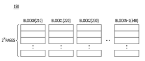
도 4는 본 발명의 실시 예에 따른 메모리 시스템에서 메모리 장치 구조를 개략적으로 도시한 도면이다.
도 5a 는 2 비트 멀티 비트 셀(MLC) 비휘발성 메모리 장치의 프로그램 상태 및 소거 상태를 나타내는 이상적인 문턱 전압 산포 그래프이다.
도 5b는 2 비트 멀티 비트 셀(MLC) 비휘발성 메모리 장치의 특성 열화로 인하여 변형될 수 있는 프로그램 상태 및 소거 상태를 나타내는 문턱 전압 산포 그래프이다.
도 6은 본 발명의 실시 예에 따른 메모리 시스템의 구조를 나타낸 도면이다.
도 7a 내지 도 7d는 본 발명의 실시 예에 따른 리드 전압 검색 동작을 나타낸 개념도이다.
도 8는 본 발명의 실시 예에 따른 메모리 시스템의 동작을 나타낸 흐름도이다.
도 9 내지 도 17은 본 발명의 실시 예에 따른 메모리 시스템을 포함하는 데이터 처리 시스템의 다른 일 예들을 개략적으로 도시한 도면이다.






Claims (20)
- 컨트롤러의 동작방법에 있어서,
민-전압 관리부에 의하여 프로그램 상태에 대응하는 소스 리드 전압으로부터 후보 민-전압을 추정하는 단계;
신뢰구간 관리부에 의하여 상기 후보 민-전압이 상기 프로그램 상태에 대응하는 신뢰구간 내에 위치하는지 판단하는 단계;
상기 신뢰구간 관리부에 의하여 상기 후보 민-전압들이 상기 신뢰구간에 위치한다면, 상기 후보 민-전압을 선택하는 단계;
리드 전압 관리부에 의하여 선택 민-전압 - 상기 선택된 후보 민-전압 - 에 기초하여 타겟 리드 전압을 검색하는 단계; 및
프로세서에 의하여 상기 타겟 리드 전압으로 타겟 데이터를 리드하는 단계
를 포함하는 컨트롤러의 동작방법.
- 제 1 항에 있어서,
상기 후보 민-전압을 추정하는 단계는
상기 소스 리드 전압과 상기 소스 리드 전압에 대응하는 상수를 활용하여 상기 후보 민-전압을 추정하는
컨트롤러의 동작방법. - 제 2 항에 있어서,
상기 소스 리드 전압에 의한 1셀의 개수, 상기 프로그램 상태에 대응하는 이상적인 민-전압에 의한 1셀의 개수 및 상기 프로그램 상태에 대응하는 전압 윈도우 폭을 활용하여 상기 상수를 계산하는 단계
를 더 포함하는 컨트롤러의 동작방법.
- 제 1 항에 있어서,
상기 후보 민-전압을 추정하는 단계는
상기 소스 리드 전압 및 가우시안 알고리즘을 활용하여 상기 후보 민-전압을 추정하는
컨트롤러의 동작방법.
- 제 1 항에 있어서,
상기 신뢰구간은 이상적인 민-전압에서 리드되는 '1'셀의 개수와 대비하여 소정의 '1'셀의 개수를 가진 전압에 대한 구간인
컨트롤러의 동작방법.
- 제 1 항에 있어서,
상기 타겟 리드 전압을 검색하는 단계는
상기 선택 민-전압의 중간값을 갖는 리드 전압을 상기 타겟 리드 전압으로서 검색하는
컨트롤러의 동작방법.
- 제 1 항에 있어서,
상기 후보 민-전압이 상기 신뢰구간 내에 위치하지 않는다면, 상기 신뢰구간 밖에 위치한 제 1 후보 민-전압에 대응하는 프로그램 상태에 대하여 가우시안 알고리즘을 활용하여 제 2 후보 민-전압을 추정하는 단계
를 더 포함하는 컨트롤러의 동작방법.
- 제 1 항에 있어서,
상기 후보 민-전압을 추정하는 단계는
상기 소스 리드 전압을 활용하여 상기 타겟 데이터를 리드하고, 상기 타겟 데이터에 대한 리드 동작을 실패한 경우에, 상기 후보 민-전압을 추정하는
컨트롤러의 동작방법. - 제 8 항에 있어서,
상기 소스 리드 전압의 초기 값은 사전 설정된 디폴트 값인
컨트롤러의 동작방법.
- 제 9 항에 있어서,
상기 소스 리드 전압은 상기 타겟 리드 전압으로 업데이트되는 단계
를 더 포함하는 컨트롤러의 동작방법.
- 프로그램 상태에 대응하는 소스 리드 전압으로부터 후보 민-전압을 추정하는 민-전압 관리부;
상기 후보 민-전압이 상기 프로그램 상태에 대응하는 신뢰구간 내에 위치하는지 판단하고, 상기 후보 민-전압들이 상기 신뢰구간에 위치한다면, 상기 후보 민-전압을 선택하는 신뢰구간 관리부;
선택 민-전압 - 상기 선택된 후보 민-전압 - 에 기초하여 타겟 리드 전압을 검색하는 리드 전압 관리부; 및
상기 검색된 타겟 리드 전압으로 타겟 데이터를 리드하는 프로세서
를 포함하는 컨트롤러. - 제 11 항에 있어서,
상기 민-전압 관리부는
상기 소스 리드 전압과 상기 소스 리드 전압에 대응하는 상수를 활용하여 상기 후보 민-전압을 추정하는
컨트롤러.
- 제 12 항에 있어서,
상기 민-전압 관리부는
상기 소스 리드 전압에 의한 1셀의 개수, 상기 프로그램 상태에 대응하는 이상적인 민-전압에 의한 1셀의 개수 및 상기 프로그램 상태에 대응하는 전압 윈도우 폭을 활용하여 상기 상수를 계산하는
컨트롤러.
- 제 11 항에 있어서,
상기 민-전압 관리부는
상기 소스 리드 전압 및 가우시안 알고리즘을 활용하여 상기 후보 민-전압을 추정하는
컨트롤러.
- 제 11 항에 있어서,
상기 신뢰구간은 이상적인 민-전압에서 리드되는 '1'셀의 개수와 대비하여 소정의 '1'셀의 개수를 가진 전압에 대한 구간인
컨트롤러.
- 제 11 항에 있어서,
상기 리드 전압 관리부는
상기 선택 민-전압의 중간값을 갖는 리드 전압을 상기 타겟 리드 전압으로서 검색하는
컨트롤러.
- 제 11 항에 있어서,
상기 민-전압 관리부는
상기 후보 민-전압이 상기 신뢰구간 내에 위치하지 않는다면, 상기 신뢰구간 밖에 위치한 제 1 후보 민-전압에 대응하는 프로그램 상태에 대하여 가우시안 알고리즘을 활용하여 제 2 후보 민-전압을 추정하는
컨트롤러.
- 제 11 항에 있어서,
상기 민-전압 관리부는
상기 소스 리드 전압을 활용하여 상기 타겟 데이터를 리드하고, 상기 타겟 데이터에 대한 리드 동작을 실패한 경우에, 상기 후보 민-전압을 추정하는
컨트롤러.
- 제 18 항에 있어서,
상기 소스 리드 전압의 초기 값은 사전 설정된 디폴트 값인
컨트롤러.
- 제 19 항에 있어서,
상기 리드 전압 관리부는
상기 타겟 리드 전압을 상기 소르 리드 전압으로서 업데이트하는 단계
컨트롤러.
Priority Applications (2)
| Application Number | Priority Date | Filing Date | Title |
|---|---|---|---|
| KR1020180097472A KR20200021736A (ko) | 2018-08-21 | 2018-08-21 | 컨트롤러 및 그것의 동작방법 |
| US16/406,144 US11049569B2 (en) | 2018-08-21 | 2019-05-08 | Controller and operating method thereof |
Applications Claiming Priority (1)
| Application Number | Priority Date | Filing Date | Title |
|---|---|---|---|
| KR1020180097472A KR20200021736A (ko) | 2018-08-21 | 2018-08-21 | 컨트롤러 및 그것의 동작방법 |
Publications (1)
| Publication Number | Publication Date |
|---|---|
| KR20200021736A true KR20200021736A (ko) | 2020-03-02 |
Family
ID=69586479
Family Applications (1)
| Application Number | Title | Priority Date | Filing Date |
|---|---|---|---|
| KR1020180097472A Ceased KR20200021736A (ko) | 2018-08-21 | 2018-08-21 | 컨트롤러 및 그것의 동작방법 |
Country Status (2)
| Country | Link |
|---|---|
| US (1) | US11049569B2 (ko) |
| KR (1) | KR20200021736A (ko) |
Families Citing this family (3)
| Publication number | Priority date | Publication date | Assignee | Title |
|---|---|---|---|---|
| US10366763B2 (en) | 2017-10-31 | 2019-07-30 | Micron Technology, Inc. | Block read count voltage adjustment |
| US11004391B2 (en) * | 2019-06-10 | 2021-05-11 | Apple Inc. | Image data compensation based on predicted changes in threshold voltage of pixel transistors |
| JP2021012752A (ja) * | 2019-07-08 | 2021-02-04 | キオクシア株式会社 | 半導体記憶装置 |
Family Cites Families (3)
| Publication number | Priority date | Publication date | Assignee | Title |
|---|---|---|---|---|
| KR101516577B1 (ko) | 2008-11-10 | 2015-05-06 | 삼성전자주식회사 | 비휘발성 반도체 메모리 장치, 그를 포함하는 메모리 카드와 메모리 시스템 및 그의 리드 전압 추정 방법 |
| TWI612525B (zh) | 2016-07-07 | 2018-01-21 | 群聯電子股份有限公司 | 解碼方法、記憶體儲存裝置及記憶體控制電路單元 |
| TWI651721B (zh) * | 2018-03-09 | 2019-02-21 | 大陸商深圳大心電子科技有限公司 | 解碼方法以及儲存控制器 |
-
2018
- 2018-08-21 KR KR1020180097472A patent/KR20200021736A/ko not_active Ceased
-
2019
- 2019-05-08 US US16/406,144 patent/US11049569B2/en active Active
Also Published As
| Publication number | Publication date |
|---|---|
| US20200066356A1 (en) | 2020-02-27 |
| US11049569B2 (en) | 2021-06-29 |
Similar Documents
| Publication | Publication Date | Title |
|---|---|---|
| KR102671727B1 (ko) | 메모리 시스템 및 그것의 동작방법 | |
| KR102612891B1 (ko) | 메모리 장치, 그것의 동작방법 및 메모리 시스템 | |
| KR102532563B1 (ko) | 메모리 장치 및 그것의 동작방법 | |
| KR20190113436A (ko) | 컨트롤러, 그것의 동작방법 및 컨트롤러를 포함하는 메모리 시스템 | |
| KR102737416B1 (ko) | 메모리 시스템 및 그것의 동작방법 | |
| US20200210295A1 (en) | Memory system and operating method thereof | |
| KR20190128392A (ko) | 메모리 시스템 및 메모리 시스템의 동작방법 | |
| KR20200095903A (ko) | 메모리 시스템 및 그것의 동작방법 | |
| KR20200019430A (ko) | 컨트롤러 및 그것의 동작방법 | |
| US10908992B2 (en) | Controller and operation method thereof | |
| US10747664B2 (en) | Memory system and operating method thereof | |
| KR102586786B1 (ko) | 메모리 시스템 및 그것의 동작방법 | |
| KR102745797B1 (ko) | 메모리 시스템 및 그것의 동작방법 | |
| KR102659036B1 (ko) | 메모리 시스템 및 그것의 동작방법 | |
| KR102567314B1 (ko) | 메모리 시스템 및 그것의 동작방법 | |
| US11049569B2 (en) | Controller and operating method thereof | |
| KR20200015247A (ko) | 메모리 시스템 및 메모리 시스템의 동작방법 | |
| KR20190110242A (ko) | 메모리 시스템 및 메모리 시스템의 동작방법 | |
| KR20190108788A (ko) | 메모리 시스템 및 메모리 시스템의 동작방법 | |
| KR102697321B1 (ko) | 메모리 시스템 및 그것의 동작방법 | |
| KR102513498B1 (ko) | 컨트롤러, 그것의 동작방법 및 컨트롤러를 포함하는 메모리 시스템 | |
| KR20200023758A (ko) | 메모리 시스템 및 그것의 동작방법 | |
| KR20190099590A (ko) | 메모리 시스템 및 메모리 시스템의 동작방법 | |
| KR102689927B1 (ko) | 메모리 시스템 및 그것의 동작방법 | |
| KR102654308B1 (ko) | 메모리 시스템 및 그것의 동작방법 |
Legal Events
| Date | Code | Title | Description |
|---|---|---|---|
| PA0109 | Patent application |
Patent event code: PA01091R01D Comment text: Patent Application Patent event date: 20180821 |
|
| PG1501 | Laying open of application | ||
| A201 | Request for examination | ||
| PA0201 | Request for examination |
Patent event code: PA02012R01D Patent event date: 20210810 Comment text: Request for Examination of Application Patent event code: PA02011R01I Patent event date: 20180821 Comment text: Patent Application |
|
| E902 | Notification of reason for refusal | ||
| PE0902 | Notice of grounds for rejection |
Comment text: Notification of reason for refusal Patent event date: 20230426 Patent event code: PE09021S01D |
|
| E902 | Notification of reason for refusal | ||
| PE0902 | Notice of grounds for rejection |
Comment text: Notification of reason for refusal Patent event date: 20231221 Patent event code: PE09021S01D |
|
| E601 | Decision to refuse application | ||
| PE0601 | Decision on rejection of patent |
Patent event date: 20240223 Comment text: Decision to Refuse Application Patent event code: PE06012S01D Patent event date: 20231221 Comment text: Notification of reason for refusal Patent event code: PE06011S01I Patent event date: 20230426 Comment text: Notification of reason for refusal Patent event code: PE06011S01I |