KR20200095903A - 메모리 시스템 및 그것의 동작방법 - Google Patents
메모리 시스템 및 그것의 동작방법 Download PDFInfo
- Publication number
- KR20200095903A KR20200095903A KR1020190013867A KR20190013867A KR20200095903A KR 20200095903 A KR20200095903 A KR 20200095903A KR 1020190013867 A KR1020190013867 A KR 1020190013867A KR 20190013867 A KR20190013867 A KR 20190013867A KR 20200095903 A KR20200095903 A KR 20200095903A
- Authority
- KR
- South Korea
- Prior art keywords
- read
- memory
- data
- target
- memory system
- Prior art date
- Legal status (The legal status is an assumption and is not a legal conclusion. Google has not performed a legal analysis and makes no representation as to the accuracy of the status listed.)
- Granted
Links
Images




Classifications
-
- G—PHYSICS
- G11—INFORMATION STORAGE
- G11C—STATIC STORES
- G11C16/00—Erasable programmable read-only memories
- G11C16/02—Erasable programmable read-only memories electrically programmable
- G11C16/06—Auxiliary circuits, e.g. for writing into memory
- G11C16/26—Sensing or reading circuits; Data output circuits
-
- G—PHYSICS
- G06—COMPUTING OR CALCULATING; COUNTING
- G06F—ELECTRIC DIGITAL DATA PROCESSING
- G06F1/00—Details not covered by groups G06F3/00 - G06F13/00 and G06F21/00
- G06F1/04—Generating or distributing clock signals or signals derived directly therefrom
- G06F1/14—Time supervision arrangements, e.g. real time clock
-
- G—PHYSICS
- G06—COMPUTING OR CALCULATING; COUNTING
- G06F—ELECTRIC DIGITAL DATA PROCESSING
- G06F11/00—Error detection; Error correction; Monitoring
- G06F11/07—Responding to the occurrence of a fault, e.g. fault tolerance
- G06F11/0703—Error or fault processing not based on redundancy, i.e. by taking additional measures to deal with the error or fault not making use of redundancy in operation, in hardware, or in data representation
- G06F11/0751—Error or fault detection not based on redundancy
- G06F11/0754—Error or fault detection not based on redundancy by exceeding limits
- G06F11/076—Error or fault detection not based on redundancy by exceeding limits by exceeding a count or rate limit, e.g. word- or bit count limit
-
- G—PHYSICS
- G06—COMPUTING OR CALCULATING; COUNTING
- G06F—ELECTRIC DIGITAL DATA PROCESSING
- G06F11/00—Error detection; Error correction; Monitoring
- G06F11/07—Responding to the occurrence of a fault, e.g. fault tolerance
- G06F11/08—Error detection or correction by redundancy in data representation, e.g. by using checking codes
- G06F11/10—Adding special bits or symbols to the coded information, e.g. parity check, casting out 9's or 11's
- G06F11/1008—Adding special bits or symbols to the coded information, e.g. parity check, casting out 9's or 11's in individual solid state devices
-
- G—PHYSICS
- G06—COMPUTING OR CALCULATING; COUNTING
- G06F—ELECTRIC DIGITAL DATA PROCESSING
- G06F11/00—Error detection; Error correction; Monitoring
- G06F11/07—Responding to the occurrence of a fault, e.g. fault tolerance
- G06F11/08—Error detection or correction by redundancy in data representation, e.g. by using checking codes
- G06F11/10—Adding special bits or symbols to the coded information, e.g. parity check, casting out 9's or 11's
- G06F11/1008—Adding special bits or symbols to the coded information, e.g. parity check, casting out 9's or 11's in individual solid state devices
- G06F11/1044—Adding special bits or symbols to the coded information, e.g. parity check, casting out 9's or 11's in individual solid state devices with specific ECC/EDC distribution
-
- G—PHYSICS
- G06—COMPUTING OR CALCULATING; COUNTING
- G06F—ELECTRIC DIGITAL DATA PROCESSING
- G06F11/00—Error detection; Error correction; Monitoring
- G06F11/07—Responding to the occurrence of a fault, e.g. fault tolerance
- G06F11/08—Error detection or correction by redundancy in data representation, e.g. by using checking codes
- G06F11/10—Adding special bits or symbols to the coded information, e.g. parity check, casting out 9's or 11's
- G06F11/1008—Adding special bits or symbols to the coded information, e.g. parity check, casting out 9's or 11's in individual solid state devices
- G06F11/1048—Adding special bits or symbols to the coded information, e.g. parity check, casting out 9's or 11's in individual solid state devices using arrangements adapted for a specific error detection or correction feature
-
- G—PHYSICS
- G06—COMPUTING OR CALCULATING; COUNTING
- G06F—ELECTRIC DIGITAL DATA PROCESSING
- G06F11/00—Error detection; Error correction; Monitoring
- G06F11/30—Monitoring
- G06F11/3003—Monitoring arrangements specially adapted to the computing system or computing system component being monitored
- G06F11/3037—Monitoring arrangements specially adapted to the computing system or computing system component being monitored where the computing system component is a memory, e.g. virtual memory, cache
-
- G—PHYSICS
- G06—COMPUTING OR CALCULATING; COUNTING
- G06F—ELECTRIC DIGITAL DATA PROCESSING
- G06F11/00—Error detection; Error correction; Monitoring
- G06F11/30—Monitoring
- G06F11/3058—Monitoring arrangements for monitoring environmental properties or parameters of the computing system or of the computing system component, e.g. monitoring of power, currents, temperature, humidity, position, vibrations
-
- G—PHYSICS
- G06—COMPUTING OR CALCULATING; COUNTING
- G06F—ELECTRIC DIGITAL DATA PROCESSING
- G06F3/00—Input arrangements for transferring data to be processed into a form capable of being handled by the computer; Output arrangements for transferring data from processing unit to output unit, e.g. interface arrangements
- G06F3/06—Digital input from, or digital output to, record carriers, e.g. RAID, emulated record carriers or networked record carriers
- G06F3/0601—Interfaces specially adapted for storage systems
- G06F3/0602—Interfaces specially adapted for storage systems specifically adapted to achieve a particular effect
- G06F3/061—Improving I/O performance
-
- G—PHYSICS
- G06—COMPUTING OR CALCULATING; COUNTING
- G06F—ELECTRIC DIGITAL DATA PROCESSING
- G06F3/00—Input arrangements for transferring data to be processed into a form capable of being handled by the computer; Output arrangements for transferring data from processing unit to output unit, e.g. interface arrangements
- G06F3/06—Digital input from, or digital output to, record carriers, e.g. RAID, emulated record carriers or networked record carriers
- G06F3/0601—Interfaces specially adapted for storage systems
- G06F3/0628—Interfaces specially adapted for storage systems making use of a particular technique
- G06F3/0655—Vertical data movement, i.e. input-output transfer; data movement between one or more hosts and one or more storage devices
- G06F3/0658—Controller construction arrangements
-
- G—PHYSICS
- G06—COMPUTING OR CALCULATING; COUNTING
- G06F—ELECTRIC DIGITAL DATA PROCESSING
- G06F3/00—Input arrangements for transferring data to be processed into a form capable of being handled by the computer; Output arrangements for transferring data from processing unit to output unit, e.g. interface arrangements
- G06F3/06—Digital input from, or digital output to, record carriers, e.g. RAID, emulated record carriers or networked record carriers
- G06F3/0601—Interfaces specially adapted for storage systems
- G06F3/0628—Interfaces specially adapted for storage systems making use of a particular technique
- G06F3/0655—Vertical data movement, i.e. input-output transfer; data movement between one or more hosts and one or more storage devices
- G06F3/0659—Command handling arrangements, e.g. command buffers, queues, command scheduling
-
- G—PHYSICS
- G11—INFORMATION STORAGE
- G11C—STATIC STORES
- G11C11/00—Digital stores characterised by the use of particular electric or magnetic storage elements; Storage elements therefor
- G11C11/21—Digital stores characterised by the use of particular electric or magnetic storage elements; Storage elements therefor using electric elements
- G11C11/34—Digital stores characterised by the use of particular electric or magnetic storage elements; Storage elements therefor using electric elements using semiconductor devices
- G11C11/40—Digital stores characterised by the use of particular electric or magnetic storage elements; Storage elements therefor using electric elements using semiconductor devices using transistors
- G11C11/401—Digital stores characterised by the use of particular electric or magnetic storage elements; Storage elements therefor using electric elements using semiconductor devices using transistors forming cells needing refreshing or charge regeneration, i.e. dynamic cells
- G11C11/4063—Auxiliary circuits, e.g. for addressing, decoding, driving, writing, sensing or timing
- G11C11/407—Auxiliary circuits, e.g. for addressing, decoding, driving, writing, sensing or timing for memory cells of the field-effect type
- G11C11/4074—Power supply or voltage generation circuits, e.g. bias voltage generators, substrate voltage generators, back-up power, power control circuits
-
- G—PHYSICS
- G11—INFORMATION STORAGE
- G11C—STATIC STORES
- G11C16/00—Erasable programmable read-only memories
- G11C16/02—Erasable programmable read-only memories electrically programmable
- G11C16/06—Auxiliary circuits, e.g. for writing into memory
- G11C16/34—Determination of programming status, e.g. threshold voltage, overprogramming or underprogramming, retention
- G11C16/3418—Disturbance prevention or evaluation; Refreshing of disturbed memory data
-
- G—PHYSICS
- G11—INFORMATION STORAGE
- G11C—STATIC STORES
- G11C29/00—Checking stores for correct operation ; Subsequent repair; Testing stores during standby or offline operation
- G11C29/04—Detection or location of defective memory elements, e.g. cell constructio details, timing of test signals
- G11C29/08—Functional testing, e.g. testing during refresh, power-on self testing [POST] or distributed testing
- G11C29/12—Built-in arrangements for testing, e.g. built-in self testing [BIST] or interconnection details
- G11C29/38—Response verification devices
- G11C29/42—Response verification devices using error correcting codes [ECC] or parity check
-
- G—PHYSICS
- G11—INFORMATION STORAGE
- G11C—STATIC STORES
- G11C7/00—Arrangements for writing information into, or reading information out from, a digital store
- G11C7/04—Arrangements for writing information into, or reading information out from, a digital store with means for avoiding disturbances due to temperature effects
-
- G—PHYSICS
- G06—COMPUTING OR CALCULATING; COUNTING
- G06F—ELECTRIC DIGITAL DATA PROCESSING
- G06F11/00—Error detection; Error correction; Monitoring
- G06F11/07—Responding to the occurrence of a fault, e.g. fault tolerance
- G06F11/14—Error detection or correction of the data by redundancy in operations
- G06F11/1402—Saving, restoring, recovering or retrying
-
- G—PHYSICS
- G06—COMPUTING OR CALCULATING; COUNTING
- G06F—ELECTRIC DIGITAL DATA PROCESSING
- G06F2201/00—Indexing scheme relating to error detection, to error correction, and to monitoring
- G06F2201/81—Threshold
-
- G—PHYSICS
- G11—INFORMATION STORAGE
- G11C—STATIC STORES
- G11C16/00—Erasable programmable read-only memories
- G11C16/02—Erasable programmable read-only memories electrically programmable
- G11C16/04—Erasable programmable read-only memories electrically programmable using variable threshold transistors, e.g. FAMOS
- G11C16/0483—Erasable programmable read-only memories electrically programmable using variable threshold transistors, e.g. FAMOS comprising cells having several storage transistors connected in series
-
- G—PHYSICS
- G11—INFORMATION STORAGE
- G11C—STATIC STORES
- G11C29/00—Checking stores for correct operation ; Subsequent repair; Testing stores during standby or offline operation
- G11C29/04—Detection or location of defective memory elements, e.g. cell constructio details, timing of test signals
- G11C2029/0409—Online test
-
- G—PHYSICS
- G11—INFORMATION STORAGE
- G11C—STATIC STORES
- G11C29/00—Checking stores for correct operation ; Subsequent repair; Testing stores during standby or offline operation
- G11C29/04—Detection or location of defective memory elements, e.g. cell constructio details, timing of test signals
- G11C2029/0411—Online error correction
Landscapes
- Engineering & Computer Science (AREA)
- Theoretical Computer Science (AREA)
- Physics & Mathematics (AREA)
- General Engineering & Computer Science (AREA)
- General Physics & Mathematics (AREA)
- Quality & Reliability (AREA)
- Computing Systems (AREA)
- Human Computer Interaction (AREA)
- Mathematical Physics (AREA)
- Microelectronics & Electronic Packaging (AREA)
- Computer Hardware Design (AREA)
- Read Only Memory (AREA)
- Techniques For Improving Reliability Of Storages (AREA)
Abstract
Description
도 2는 본 발명의 실시 예에 따른 메모리 시스템에서 메모리 장치의 일 예를 개략적으로 도시한 도면이다.
도 3는 메모리 장치 내 메모리 셀의 산포를 나타낸 도면이다.
도 4a 및 도 4b는 메모리 셀의 특성 열화로 인하여 변형된 메모리 셀의 상태를 나타낸 도면이다.
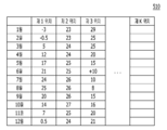
도 5a는 본 발명의 실시 예에 따른 온도 테이블을 나타낸다.
도 5b는 본 발명의 실시 예에 따른 리드 전압 테이블을 나타낸다.
도 6 는 본 발명의 실시 예에 따른 리드 동작을 나타낸 흐름도이다.
도 7은 본 발명의 실시 예에 따른 리드 리트라이 동작을 나태는 흐름도이다.
도 8 내지 도 11은 본 발명의 실시 예에 따른 메모리 시스템을 포함하는 데이터 처리 시스템의 다른 일 예들을 개략적으로 도시한 도면이다.
Claims (20)
- 메모리 시스템에 있어서,
복수의 메모리 셀들을 포함하는 메모리 장치; 및
호스트로부터 제공된 리드 커맨드에 대응하는 데이터가 저장된 타겟 메모리 셀에 제 1 리드 전압을 인가하여 제 1 리드 동작을 수행하도록 상기 메모리 장치를 제어하는 컨트롤러
를 포함하고,
상기 컨트롤러는
상기 제 1 리드 데이터 - 상기 제 1 리드 동작에 의하여 리드된 데이터- 의 페일 비트가 사전 설정된 임계 값보다 크거나 같은 경우, 상기 호스트로부터 제공된 RTC 정보 및 위치 정보에 기초하여 온도 테이블 내 기록된 외부 온도를 확인하고, 상기 외부 온도 및 리드 전압 테이블에 기초하여 제 2 리드 전압을 설정하며, 상기 제 2 리드 전압을 활용하여 상기 데이터에 대하여 제 2 리드동작을 수행하는
메모리 시스템.
- 제 1 항에 있어서,
상기 온도 테이블은 복수의 위치 정보 각각의 '월'(month) 평균 온도를 나타내며,
상기 리드 전압 테이블은 복수의 온도 구간들, 상기 복수의 온도 구간들 각각에 포함된 복수의 인덱스들 및 상기 복수의 인덱스들 각각에 대응하는 리드 전압을 나타내는
메모리 시스템.
- 제 1 항에 있어서,
상기 컨트롤러는
상기 온도 테이블 및 상기 리드 전압 테이블을 저장하는 메모리,
상기 제 1 리드 데이터에 대한 디코딩 동작을 통하여 상기 페일 비트 수를 카운트하고, 상기 페일 비트 수와 사전 설정된 임계 값을 비교하는 ECC 유닛, 및
상기 제 1 리드 데이터의 페일 비트가 사전 설정된 임계 값보다 크거나 같은 경우, 상기 외부 온도를 확인하고, 상기 제 2 리드 전압을 설정하며, 상기 제 2 리드 전압을 상기 타겟 메모리 셀에 인가하여 상기 제 2 리드동작을 수행하도록 상기 메모리 장치를 제어하는 프로세서
를 포함하는 메모리 시스템.
- 제 2 항에 있어서,
상기 컨트롤러는
상기 리드 전압 테이블에 포함된 복수의 온도 구간들 중 상기 외부 온도가 포함된 타겟 온도 구간을 확인하는
메모리 시스템.
- 제 4 항에 있어서,
상기 컨트롤러는
상기 타겟 온도 구간에 포함된 복수의 인덱스들 중에서 상기 외부 온도에 기초하여 타겟 인덱스를 선택하는
메모리 시스템.
- 제 5 항에 있어서,
상기 컨트롤러는
상기 타겟 인덱스에 포함된 전압을 상기 제 2 리드 전압으로 설정하고, 상기 제 2 리드 전압을 상기 타겟 메모리 셀에 인가하여 상기 제 2 리드 동작을 수행하도록 상기 메모리 장치를 제어하는
메모리 시스템.
- 제 6 항에 있어서,
상기 컨트롤러는
제 2 리드 데이터 - 상기 제 2 리드 동작에 의하여 리드된 데이터 - 에 대한 디코딩 동작을 수행하고, 상기 제 2 리드 데이터의 페일 비트 수가 사전 설정된 임계 값보다 크거나 같은 경우, 상기 타겟 인덱스가 상기 타겟 엔트리 내 마지막 인덱스인지 확인하는
메모리 시스템.
- 제 7 항에 있어서,
상기 컨트롤러는
상기 타겟 인덱스가 상기 타겟 엔트리 내 마지막 인덱스가 아니라면, 상기 타겟 엔트리 내에서 타겟 인덱스의 다음 인덱스에 포함된 전압을 제 3 리드 전압으로 설정하고, 상기 제 3 리드 전압을 상기 타겟 메모리 셀에 인가하여 제 3 리드동작을 수행하도록 상기 메모리 장치를 제어하는
메모리 시스템.
- 제 7 항에 있어서,
상기 컨트롤러는
상기 타겟 인덱스가 상기 타겟 엔트리 내 마지막 인덱스라면, 상기 데이터에 대한 리드 실패를 상기 호스트에 통지하는
메모리 시스템.
- 제 7 항에 있어서,
상기 컨트롤러는
상기 제 2 리드 데이터의 페일 비트 수가 사전 설정된 임계 값보다 작은 경우, 상기 제 2 데이터를 상기 리드 커맨드에 응답하여 상기 호스트로 제공하는
메모리 시스템.
- 메모리 시스템의 동작방법에 있어서,
호스트로부터 RTC 정보 및 위치 정보를 제공받는 단계;
상기 호스트로부터 제공된 리드 커맨드에 대응하는 데이터가 저장된 타겟 메모리 셀에 제 1 리드 전압을 인가하여 제 1 리드 동작을 수행하는 단계;
상기 제 1 리드 데이터 - 상기 제 1 리드 동작에 의하여 리드된 데이터 -의 페일 비트가 사전 설정된 임계 값보다 크거나 같은 경우, 상기 RTC 정보 및 상기 위치 정보에 기초하여 온도 테이블 내 기록된 외부 온도를 확인하는 단계;
상기 외부 온도 및 리드 전압 테이블에 기초하여 제 2 리드 전압을 설정하는 단계; 및
상기 제 2 리드 전압을 상기 타겟 메모리 셀에 인가하여 제 2 리드 동작을 수행하는 단계
를 포함하는 메모리 시스템의 동작방법.
- 제 11 항에 있어서,
상기 온도 테이블은 복수의 위치 정보 각각의 '월'(month) 평균 온도를 나타내며,
상기 리드 전압 테이블은 복수의 온도 구간들, 상기 복수의 온도 구간들 각각에 포함된 복수의 인덱스들 및 상기 복수의 인덱스들 각각에 대응하는 리드 전압을 나타내는
메모리 시스템의 동작방법.
- 제 11 항에 있어서,
상기 온도 테이블 및 상기 리드 전압 테이블을 저장하는 단계;
상기 제 1 리드 데이터에 대한 디코딩 동작을 수행하여 상기 제 1 리드 데이터의 페일 비트 수를 카운트하는 단계;
상기 제 1 리드 데이터의 페일 비트 수와 사전 설정된 임계 값을 비교하는 단계
를 더 포함하는 메모리 시스템의 동작방법.
- 제 12 항에 있어서,
상기 제 2 리드 전압을 설정하는 단계는
상기 리드 전압 테이블에 포함된 복수의 온도 구간들 중 상기 외부 온도가 포함된 타겟 온도 구간을 확인하는 단계
를 포함하는 메모리 시스템의 동작방법.
- 제 14 항에 있어서,
상기 제 2 리드 전압을 설정하는 단계는
상기 타겟 온도 구간에 포함된 복수의 인덱스들 중에서 상기 외부온도에 기초하여 타겟 인덱스를 선택하고, 상기 타겟 인덱스에 포함된 전압을 상기 제 2 리드 전압으로 설정하는 단계
를 포함하는 메모리 시스템의 동작방법.
- 제 15 항에 있어서,
상기 제 2 리드 동작을 수행하는 단계는
상기 타겟 인덱스에 포함된 전압을 제 2 리드 전압으로 활용하여 상기 제 2 리드 동작을 수행하는
메모리 시스템의 동작방법.
- 제 16 항에 있어서,
제 2 리드 데이터 - 상기 제 2 리드 동작에 의하여 리드된 데이터 - 에 대한 디코딩 동작을 수행하는 단계; 및
상기 제 2 리드 데이터의 페일 비트 수가 사전 설정된 임계 값보다 크거나 같은 경우, 상기 타겟 인덱스가 상기 타겟 엔트리 내 마지막 인덱스인지 확인하는 단계
를 더 포함하는 메모리 시스템의 동작방법.
- 제 17 항에 있어서,
상기 타겟 인덱스가 상기 타겟 엔트리 내 마지막 인덱스가 아니라면, 상기 타겟 엔트리 내에서 타겟 인덱스의 다음 인덱스에 포함된 전압을 제 3 리드 전압으로 설정하는 단계; 및
상기 제 3 리드 전압을 상기 타겟 메모리 셀에 인가하여 제 3 리드 동작을 수행하는 단계
를 더 포함하는 메모리 시스템의 동작방법.
- 제 17 항에 있어서,
상기 타겟 인덱스가 상기 타겟 엔트리 내 마지막 인덱스라면, 상기 데이터에 대한 리드 실패를 상기 호스트에 통지하는 단계
를 더 포함하는 메모리 시스템의 동작방법.
- 제 17 항에 있어서,
상기 제 2 리드 데이터의 페일 비트 수가 사전 설정된 임계 값보다 작은 경우, 상기 제 2 리드 데이터를 상기 호스트로 제공하는 단계
를 더 포함하는 메모리 시스템의 동작방법.
Priority Applications (3)
| Application Number | Priority Date | Filing Date | Title |
|---|---|---|---|
| KR1020190013867A KR102714121B1 (ko) | 2019-02-01 | 2019-02-01 | 메모리 시스템 및 그것의 동작방법 |
| CN201911300224.3A CN111540399A (zh) | 2019-02-01 | 2019-12-16 | 存储器系统及其操作方法 |
| US16/723,075 US11334462B2 (en) | 2019-02-01 | 2019-12-20 | Memory system and operating method thereof |
Applications Claiming Priority (1)
| Application Number | Priority Date | Filing Date | Title |
|---|---|---|---|
| KR1020190013867A KR102714121B1 (ko) | 2019-02-01 | 2019-02-01 | 메모리 시스템 및 그것의 동작방법 |
Publications (2)
| Publication Number | Publication Date |
|---|---|
| KR20200095903A true KR20200095903A (ko) | 2020-08-11 |
| KR102714121B1 KR102714121B1 (ko) | 2024-10-08 |
Family
ID=71836473
Family Applications (1)
| Application Number | Title | Priority Date | Filing Date |
|---|---|---|---|
| KR1020190013867A Active KR102714121B1 (ko) | 2019-02-01 | 2019-02-01 | 메모리 시스템 및 그것의 동작방법 |
Country Status (3)
| Country | Link |
|---|---|
| US (1) | US11334462B2 (ko) |
| KR (1) | KR102714121B1 (ko) |
| CN (1) | CN111540399A (ko) |
Cited By (3)
| Publication number | Priority date | Publication date | Assignee | Title |
|---|---|---|---|---|
| US11842067B2 (en) | 2021-10-20 | 2023-12-12 | SK Hynix Inc. | Memory controller, memory system including the same, and method of operating the memory system |
| US11978519B2 (en) | 2021-07-06 | 2024-05-07 | SK Hynix Inc. | Storage device and operating method thereof |
| US12417032B2 (en) | 2022-11-14 | 2025-09-16 | SK Hynix Inc. | Memory for improving performance of read retry operation, storage device, and method for operating storage device |
Families Citing this family (5)
| Publication number | Priority date | Publication date | Assignee | Title |
|---|---|---|---|---|
| US11681469B2 (en) * | 2021-02-22 | 2023-06-20 | Micron Technology, Inc. | Storing and recovering critical data in a memory device |
| US12169640B2 (en) * | 2022-08-16 | 2024-12-17 | Yangtze Memory Technologies Co., Ltd. | Read retry method for enhancing read performance and stability of 3D NAND memory |
| US12430206B2 (en) | 2023-05-19 | 2025-09-30 | Micron Technology, Inc. | Temperature sensor management during error handling operations in a memory sub-system |
| US12530134B2 (en) * | 2024-07-10 | 2026-01-20 | Lenovo (Singapore) Pte. Ltd. | Adaptive method to efficiently read out retention degraded NAND data |
| CN118571286A (zh) * | 2024-08-05 | 2024-08-30 | 新存科技(武汉)有限责任公司 | 存储器装置及存储器系统 |
Citations (3)
| Publication number | Priority date | Publication date | Assignee | Title |
|---|---|---|---|---|
| KR20170076883A (ko) * | 2015-12-24 | 2017-07-05 | 에스케이하이닉스 주식회사 | 메모리 시스템 및 그의 동작방법 |
| KR20170111375A (ko) * | 2016-03-28 | 2017-10-12 | 에스케이하이닉스 주식회사 | 메모리 시스템 및 그의 동작 방법 |
| US20190371402A1 (en) * | 2018-06-05 | 2019-12-05 | Western Digital Technologies, Inc. | Multi-sensing scan for cross-temperature mitigation |
Family Cites Families (17)
| Publication number | Priority date | Publication date | Assignee | Title |
|---|---|---|---|---|
| CN100345076C (zh) * | 2003-12-24 | 2007-10-24 | 鸿富锦精密工业(深圳)有限公司 | 电池供电式存储器电量测量系统及方法 |
| US20070255937A1 (en) * | 2006-04-26 | 2007-11-01 | Sheng-Hsin Lo | Basic input / output system (BIOS) set-value access method |
| KR101737020B1 (ko) * | 2009-09-09 | 2017-05-29 | 마벨 월드 트레이드 리미티드 | 다중 파워서플라이들 및/또는 다중 저전력 모드들을 갖는 메모리 |
| CN102142186B (zh) * | 2011-03-01 | 2013-01-09 | 合肥国轩高科动力能源有限公司 | 锂电池组远程监控系统 |
| US8472274B2 (en) * | 2011-03-02 | 2013-06-25 | Apple Inc. | Using temperature sensors with a memory device |
| CN102263303B (zh) * | 2011-06-02 | 2016-09-14 | 福州天和新能电子科技有限公司 | 模块化锂动力电池及其管理系统和管理方法 |
| KR102306804B1 (ko) | 2015-01-21 | 2021-09-30 | 삼성전자주식회사 | 전자 장치의 소모 전력 감소 방법 및 장치 |
| KR102291806B1 (ko) | 2015-04-20 | 2021-08-24 | 삼성전자주식회사 | 불휘발성 메모리 시스템 및 그것의 동작 방법 |
| CN205787727U (zh) * | 2016-05-23 | 2016-12-07 | 深圳市恒昌通电子有限公司 | 适用于无人机的集成主控器 |
| KR102695928B1 (ko) | 2016-12-19 | 2024-08-16 | 삼성전자주식회사 | 비휘발성 메모리의 리드 동작 방법, 비휘발성 메모리를 포함하는 메모리 시스템 및 이의 동작 방법 |
| US10304559B2 (en) * | 2016-12-30 | 2019-05-28 | Western Digital Technologies, Inc. | Memory write verification using temperature compensation |
| CN106679703B (zh) * | 2017-02-24 | 2022-11-08 | 河北稳控科技有限公司 | 一种振弦式传感器的读取数据装置及其工作方法 |
| KR20190001300A (ko) * | 2017-06-27 | 2019-01-04 | 에스케이하이닉스 주식회사 | 컨트롤러 및 메모리 시스템 및 메모리 시스템의 동작 방법 |
| US10535383B2 (en) * | 2018-02-28 | 2020-01-14 | Sandisk Technologies Llc | Throughput performance for cross temperature handling scenarios |
| CN109062145A (zh) * | 2018-08-13 | 2018-12-21 | 大古智能科技(上海)有限公司 | 基于wifi通信的数控机床运动控制卡 |
| US11250926B2 (en) * | 2019-10-16 | 2022-02-15 | Sandisk Technologies Llc | Positive feedback and parallel searching enhanced optimal read method for non-volatile memory |
| US11037641B1 (en) * | 2019-12-05 | 2021-06-15 | Sandisk Technologies Llc | Temperature and cycling dependent refresh operation for memory cells |
-
2019
- 2019-02-01 KR KR1020190013867A patent/KR102714121B1/ko active Active
- 2019-12-16 CN CN201911300224.3A patent/CN111540399A/zh not_active Withdrawn
- 2019-12-20 US US16/723,075 patent/US11334462B2/en active Active
Patent Citations (3)
| Publication number | Priority date | Publication date | Assignee | Title |
|---|---|---|---|---|
| KR20170076883A (ko) * | 2015-12-24 | 2017-07-05 | 에스케이하이닉스 주식회사 | 메모리 시스템 및 그의 동작방법 |
| KR20170111375A (ko) * | 2016-03-28 | 2017-10-12 | 에스케이하이닉스 주식회사 | 메모리 시스템 및 그의 동작 방법 |
| US20190371402A1 (en) * | 2018-06-05 | 2019-12-05 | Western Digital Technologies, Inc. | Multi-sensing scan for cross-temperature mitigation |
Cited By (3)
| Publication number | Priority date | Publication date | Assignee | Title |
|---|---|---|---|---|
| US11978519B2 (en) | 2021-07-06 | 2024-05-07 | SK Hynix Inc. | Storage device and operating method thereof |
| US11842067B2 (en) | 2021-10-20 | 2023-12-12 | SK Hynix Inc. | Memory controller, memory system including the same, and method of operating the memory system |
| US12417032B2 (en) | 2022-11-14 | 2025-09-16 | SK Hynix Inc. | Memory for improving performance of read retry operation, storage device, and method for operating storage device |
Also Published As
| Publication number | Publication date |
|---|---|
| KR102714121B1 (ko) | 2024-10-08 |
| US20200250061A1 (en) | 2020-08-06 |
| CN111540399A (zh) | 2020-08-14 |
| US11334462B2 (en) | 2022-05-17 |
Similar Documents
| Publication | Publication Date | Title |
|---|---|---|
| KR102714121B1 (ko) | 메모리 시스템 및 그것의 동작방법 | |
| KR102671727B1 (ko) | 메모리 시스템 및 그것의 동작방법 | |
| KR102532563B1 (ko) | 메모리 장치 및 그것의 동작방법 | |
| KR20190044798A (ko) | 컨트롤러 및 컨트롤러의 동작방법 | |
| KR102737416B1 (ko) | 메모리 시스템 및 그것의 동작방법 | |
| US11922065B2 (en) | Memory system and operating method thereof | |
| KR20200074647A (ko) | 메모리 시스템 및 그것의 동작방법 | |
| KR20200068944A (ko) | 메모리 시스템 및 그것의 동작방법 | |
| KR20180076425A (ko) | 컨트롤러 및 컨트롤러의 동작 방법 | |
| KR20200019430A (ko) | 컨트롤러 및 그것의 동작방법 | |
| KR102725203B1 (ko) | 데이터 처리 시스템 및 그의 동작방법 | |
| KR102586786B1 (ko) | 메모리 시스템 및 그것의 동작방법 | |
| KR20190102837A (ko) | 메모리 시스템 및 메모리 시스템의 동작방법 | |
| KR102567314B1 (ko) | 메모리 시스템 및 그것의 동작방법 | |
| KR102733890B1 (ko) | 메모리 시스템 및 그것의 동작방법 | |
| KR102730162B1 (ko) | 메모리 시스템 및 그것의 동작방법 | |
| KR102513498B1 (ko) | 컨트롤러, 그것의 동작방법 및 컨트롤러를 포함하는 메모리 시스템 | |
| KR102697321B1 (ko) | 메모리 시스템 및 그것의 동작방법 | |
| KR102529710B1 (ko) | 메모리 시스템 및 메모리 시스템의 동작방법 | |
| KR20200032921A (ko) | 메모리 시스템 및 그것의 동작방법 | |
| KR20200021736A (ko) | 컨트롤러 및 그것의 동작방법 | |
| KR102689927B1 (ko) | 메모리 시스템 및 그것의 동작방법 | |
| KR20190082513A (ko) | 컨트롤러 및 그것의 동작방법 | |
| KR102654308B1 (ko) | 메모리 시스템 및 그것의 동작방법 | |
| KR102704708B1 (ko) | 메모리 시스템 및 그것의 동작방법 |
Legal Events
| Date | Code | Title | Description |
|---|---|---|---|
| PA0109 | Patent application |
Patent event code: PA01091R01D Comment text: Patent Application Patent event date: 20190201 |
|
| PG1501 | Laying open of application | ||
| A201 | Request for examination | ||
| PA0201 | Request for examination |
Patent event code: PA02012R01D Patent event date: 20220119 Comment text: Request for Examination of Application Patent event code: PA02011R01I Patent event date: 20190201 Comment text: Patent Application |
|
| E902 | Notification of reason for refusal | ||
| PE0902 | Notice of grounds for rejection |
Comment text: Notification of reason for refusal Patent event date: 20231121 Patent event code: PE09021S01D |
|
| PE0701 | Decision of registration |
Patent event code: PE07011S01D Comment text: Decision to Grant Registration Patent event date: 20240705 |
|
| GRNT | Written decision to grant | ||
| PR0701 | Registration of establishment |
Comment text: Registration of Establishment Patent event date: 20240930 Patent event code: PR07011E01D |
|
| PR1002 | Payment of registration fee |
Payment date: 20241002 End annual number: 3 Start annual number: 1 |
|
| PG1601 | Publication of registration |