KR20200027902A - Structure and method for sic based protection device - Google Patents
Structure and method for sic based protection device Download PDFInfo
- Publication number
- KR20200027902A KR20200027902A KR1020190109505A KR20190109505A KR20200027902A KR 20200027902 A KR20200027902 A KR 20200027902A KR 1020190109505 A KR1020190109505 A KR 1020190109505A KR 20190109505 A KR20190109505 A KR 20190109505A KR 20200027902 A KR20200027902 A KR 20200027902A
- Authority
- KR
- South Korea
- Prior art keywords
- type
- region
- layer
- type region
- sic
- Prior art date
- Legal status (The legal status is an assumption and is not a legal conclusion. Google has not performed a legal analysis and makes no representation as to the accuracy of the status listed.)
- Granted
Links
Images


Classifications
-
- H—ELECTRICITY
- H10—SEMICONDUCTOR DEVICES; ELECTRIC SOLID-STATE DEVICES NOT OTHERWISE PROVIDED FOR
- H10D—INORGANIC ELECTRIC SEMICONDUCTOR DEVICES
- H10D8/00—Diodes
- H10D8/411—PN diodes having planar bodies
-
- H—ELECTRICITY
- H10—SEMICONDUCTOR DEVICES; ELECTRIC SOLID-STATE DEVICES NOT OTHERWISE PROVIDED FOR
- H10D—INORGANIC ELECTRIC SEMICONDUCTOR DEVICES
- H10D8/00—Diodes
- H10D8/422—PN diodes having the PN junctions in mesas
-
- H01L29/8611—
-
- H01L21/02378—
-
- H01L21/265—
-
- H01L29/0615—
-
- H01L29/66136—
-
- H—ELECTRICITY
- H10—SEMICONDUCTOR DEVICES; ELECTRIC SOLID-STATE DEVICES NOT OTHERWISE PROVIDED FOR
- H10D—INORGANIC ELECTRIC SEMICONDUCTOR DEVICES
- H10D62/00—Semiconductor bodies, or regions thereof, of devices having potential barriers
- H10D62/10—Shapes, relative sizes or dispositions of the regions of the semiconductor bodies; Shapes of the semiconductor bodies
- H10D62/102—Constructional design considerations for preventing surface leakage or controlling electric field concentration
- H10D62/103—Constructional design considerations for preventing surface leakage or controlling electric field concentration for increasing or controlling the breakdown voltage of reverse-biased devices
- H10D62/105—Constructional design considerations for preventing surface leakage or controlling electric field concentration for increasing or controlling the breakdown voltage of reverse-biased devices by having particular doping profiles, shapes or arrangements of PN junctions; by having supplementary regions, e.g. junction termination extension [JTE]
- H10D62/108—Constructional design considerations for preventing surface leakage or controlling electric field concentration for increasing or controlling the breakdown voltage of reverse-biased devices by having particular doping profiles, shapes or arrangements of PN junctions; by having supplementary regions, e.g. junction termination extension [JTE] having localised breakdown regions, e.g. built-in avalanching regions
-
- H—ELECTRICITY
- H10—SEMICONDUCTOR DEVICES; ELECTRIC SOLID-STATE DEVICES NOT OTHERWISE PROVIDED FOR
- H10D—INORGANIC ELECTRIC SEMICONDUCTOR DEVICES
- H10D62/00—Semiconductor bodies, or regions thereof, of devices having potential barriers
- H10D62/10—Shapes, relative sizes or dispositions of the regions of the semiconductor bodies; Shapes of the semiconductor bodies
- H10D62/129—Cathode regions of diodes
-
- H—ELECTRICITY
- H10—SEMICONDUCTOR DEVICES; ELECTRIC SOLID-STATE DEVICES NOT OTHERWISE PROVIDED FOR
- H10D—INORGANIC ELECTRIC SEMICONDUCTOR DEVICES
- H10D62/00—Semiconductor bodies, or regions thereof, of devices having potential barriers
- H10D62/80—Semiconductor bodies, or regions thereof, of devices having potential barriers characterised by the materials
- H10D62/83—Semiconductor bodies, or regions thereof, of devices having potential barriers characterised by the materials being Group IV materials, e.g. B-doped Si or undoped Ge
- H10D62/832—Semiconductor bodies, or regions thereof, of devices having potential barriers characterised by the materials being Group IV materials, e.g. B-doped Si or undoped Ge being Group IV materials comprising two or more elements, e.g. SiGe
- H10D62/8325—Silicon carbide
-
- H—ELECTRICITY
- H10—SEMICONDUCTOR DEVICES; ELECTRIC SOLID-STATE DEVICES NOT OTHERWISE PROVIDED FOR
- H10D—INORGANIC ELECTRIC SEMICONDUCTOR DEVICES
- H10D8/00—Diodes
- H10D8/01—Manufacture or treatment
- H10D8/021—Manufacture or treatment of breakdown diodes
- H10D8/022—Manufacture or treatment of breakdown diodes of Zener diodes
-
- H—ELECTRICITY
- H10—SEMICONDUCTOR DEVICES; ELECTRIC SOLID-STATE DEVICES NOT OTHERWISE PROVIDED FOR
- H10D—INORGANIC ELECTRIC SEMICONDUCTOR DEVICES
- H10D8/00—Diodes
- H10D8/01—Manufacture or treatment
- H10D8/045—Manufacture or treatment of PN junction diodes
-
- H—ELECTRICITY
- H10—SEMICONDUCTOR DEVICES; ELECTRIC SOLID-STATE DEVICES NOT OTHERWISE PROVIDED FOR
- H10D—INORGANIC ELECTRIC SEMICONDUCTOR DEVICES
- H10D8/00—Diodes
- H10D8/20—Breakdown diodes, e.g. avalanche diodes
- H10D8/25—Zener diodes
-
- H—ELECTRICITY
- H10—SEMICONDUCTOR DEVICES; ELECTRIC SOLID-STATE DEVICES NOT OTHERWISE PROVIDED FOR
- H10P—GENERIC PROCESSES OR APPARATUS FOR THE MANUFACTURE OR TREATMENT OF DEVICES COVERED BY CLASS H10
- H10P14/00—Formation of materials, e.g. in the shape of layers or pillars
- H10P14/20—Formation of materials, e.g. in the shape of layers or pillars of semiconductor materials
- H10P14/29—Formation of materials, e.g. in the shape of layers or pillars of semiconductor materials characterised by the substrates
- H10P14/2901—Materials
- H10P14/2902—Materials being Group IVA materials
- H10P14/2904—Silicon carbide
-
- H—ELECTRICITY
- H10—SEMICONDUCTOR DEVICES; ELECTRIC SOLID-STATE DEVICES NOT OTHERWISE PROVIDED FOR
- H10P—GENERIC PROCESSES OR APPARATUS FOR THE MANUFACTURE OR TREATMENT OF DEVICES COVERED BY CLASS H10
- H10P14/00—Formation of materials, e.g. in the shape of layers or pillars
- H10P14/20—Formation of materials, e.g. in the shape of layers or pillars of semiconductor materials
- H10P14/34—Deposited materials, e.g. layers
- H10P14/3402—Deposited materials, e.g. layers characterised by the chemical composition
- H10P14/3404—Deposited materials, e.g. layers characterised by the chemical composition being Group IVA materials
- H10P14/3408—Silicon carbide
-
- H—ELECTRICITY
- H10—SEMICONDUCTOR DEVICES; ELECTRIC SOLID-STATE DEVICES NOT OTHERWISE PROVIDED FOR
- H10P—GENERIC PROCESSES OR APPARATUS FOR THE MANUFACTURE OR TREATMENT OF DEVICES COVERED BY CLASS H10
- H10P30/00—Ion implantation into wafers, substrates or parts of devices
- H10P30/20—Ion implantation into wafers, substrates or parts of devices into semiconductor materials, e.g. for doping
- H10P30/22—Ion implantation into wafers, substrates or parts of devices into semiconductor materials, e.g. for doping using masks
-
- H—ELECTRICITY
- H10—SEMICONDUCTOR DEVICES; ELECTRIC SOLID-STATE DEVICES NOT OTHERWISE PROVIDED FOR
- H10W—GENERIC PACKAGES, INTERCONNECTIONS, CONNECTORS OR OTHER CONSTRUCTIONAL DETAILS OF DEVICES COVERED BY CLASS H10
- H10W10/00—Isolation regions in semiconductor bodies between components of integrated devices
- H10W10/01—Manufacture or treatment
- H10W10/031—Manufacture or treatment of isolation regions comprising PN junctions
-
- H—ELECTRICITY
- H10—SEMICONDUCTOR DEVICES; ELECTRIC SOLID-STATE DEVICES NOT OTHERWISE PROVIDED FOR
- H10W—GENERIC PACKAGES, INTERCONNECTIONS, CONNECTORS OR OTHER CONSTRUCTIONAL DETAILS OF DEVICES COVERED BY CLASS H10
- H10W10/00—Isolation regions in semiconductor bodies between components of integrated devices
- H10W10/30—Isolation regions comprising PN junctions
Landscapes
- Electrodes Of Semiconductors (AREA)
- Input Circuits Of Receivers And Coupling Of Receivers And Audio Equipment (AREA)
- Silver Salt Photography Or Processing Solution Therefor (AREA)
Abstract
Description
연방 지원 연구에 관한 진술Statement on Federal Assisted Research
본 발명은 미국 국방부에 의해 수여된 계약 번호 제W911NF-15-2-0088호 하에서 정부 지원으로 이루어졌다. 미국 정부는 본 발명에서 소정의 권리를 갖는다.The present invention was made with government support under contract number W911NF-15-2-0088 awarded by the United States Department of Defense. The United States government has certain rights in this invention.
본 발명의 실시예는 일반적으로 보호 디바이스, 및 특히 SiC-기반 과도 전압 억제(Transient Voltage Suppressor; TVS) 다이오드에 관한 것이다.Embodiments of the present invention generally relate to protection devices, and in particular to SiC-based Transient Voltage Suppressor (TVS) diodes.
TVS 다이오드는 전자 회로를 과도 전압으로부터 보호하도록 설계된 보호 다이오드이다. 과도 전압은 짧은 지속기간의 전기 에너지의 서지(surge)이다. 정상 작동 동안, TVS 다이오드는 누설 전류 및 커패시턴스를 최소화하도록 설계된다. 과도 전압 동안, TVS 다이오드 작동은 서지 전류를 안전하게 방전시키도록 일어난다. TVS 다이오드의 피크 출력(PP)은 상이한 펄스 폭(td)에 대해 특성화되고 제품 데이터시트에 보고된다. 구매가능한 TVS 다이오드는 규소(Si) 기술을 기반으로 한다. Si TVS 다이오드는 상이한 응용에 대한 보호 필요성을 충족시키기 위해 상이한 항복 전압(breakdown voltage) 및 출력 정격(power rating)으로 설계된다. 주어진 항복 전압에 대해, TVS 다이오드의 피크 출력 정격은 다이(die) 크기를 증가시킴으로써 증가된다. 더 큰 다이 크기를 갖는 TVS 다이오드는 더 높은 전류 취급 능력(current handling capability) 및 그에 따른 더 높은 피크 출력 정격을 갖는다.TVS diodes are protection diodes designed to protect electronic circuits from transient voltages. Transient voltage is a surge of short duration electrical energy. During normal operation, the TVS diode is designed to minimize leakage current and capacitance. During the transient voltage, TVS diode operation occurs to safely discharge the surge current. The peak output (P P ) of the TVS diode is characterized for different pulse widths (t d ) and reported in the product datasheet. Commercially available TVS diodes are based on silicon (Si) technology. Si TVS diodes are designed with different breakdown voltages and power ratings to meet the protection needs for different applications. For a given breakdown voltage, the peak output rating of the TVS diode is increased by increasing the die size. TVS diodes with larger die sizes have higher current handling capability and hence higher peak output ratings.
일부 응용의 경우, TVS 다이오드는 높은 주위 온도에서 작동할 것으로 예상된다. 고온에서, Si TVS 다이오드는 그의 최대 작동 온도를 제한하는 높은 누설 전류를 갖는다. 고온에서는, Si 다이오드의 피크 출력 취급 능력이 감소된다. 일부 구현예에서, 각각의 Si TVS 다이오드의 출력 취급을 최소화하기 위해 다수의 Si TVS 다이오드가 직렬로 연결될 수 있다. 다수의 Si TVS 다이오드의 사용은 더 높은 회로 보호 비용을 수반한다. 구매가능한 Si TVS 다이오드는 항복 전압이 수 전압에서 대략 600 V 이하까지로 제한된다. 더 높은 항복 전압을 필요로 하는 응용의 경우, 다수의 Si TVS 다이오드가 직렬로 사용되며, 이러한 구성은 다이오드의 피크 출력 정격을 감소시킨다.For some applications, TVS diodes are expected to operate at high ambient temperatures. At high temperatures, Si TVS diodes have a high leakage current limiting their maximum operating temperature. At high temperatures, the Si diode's ability to handle peak output is reduced. In some implementations, multiple Si TVS diodes can be connected in series to minimize the output handling of each Si TVS diode. The use of multiple Si TVS diodes entails higher circuit protection costs. The commercially available Si TVS diodes have a breakdown voltage limited to several voltages up to approximately 600 V or less. For applications requiring higher breakdown voltages, multiple Si TVS diodes are used in series, and this configuration reduces the diode's peak output rating.
상기의 관점에서, 탄화규소(SiC) 기반 TVS 다이오드가 Si TVS 다이오드의 대안으로서 연구되어 왔다. 탄화규소(SiC) 기반 TVS 다이오드의 사용은 Si TVS 다이오드의 단점들 중 일부를 해결할 것으로 예상된다. 우선, SiC의 큰 밴드갭(Si에 대한 1.1 eV 대비 3.26 eV)으로 인해, SiC는 Si에 비해 더 낮은 고유 캐리어 농도(intrinsic carrier concentration)를 갖는다. 더 낮은 고유 캐리어 농도로 인해, SiC 다이오드는 더 낮은 누설 전류를 갖는 Si 다이오드에 비해 더 높은 온도에서 작동될 수 있다. 우수한 재료 특성으로 인해, SiC TVS 다이오드는 Si TVS 다이오드에 비해 더 높은 피크 출력 정격을 가질 것으로 예상된다.In view of the above, silicon carbide (SiC) based TVS diodes have been studied as an alternative to Si TVS diodes. The use of silicon carbide (SiC) based TVS diodes is expected to address some of the shortcomings of Si TVS diodes. First, due to the large bandgap of SiC (3.26 eV versus 1.1 eV for Si), SiC has a lower intrinsic carrier concentration compared to Si. Due to the lower intrinsic carrier concentration, SiC diodes can operate at higher temperatures than Si diodes with lower leakage currents. Due to good material properties, SiC TVS diodes are expected to have higher peak output ratings than Si TVS diodes.
SiC에 기초한 공지의 TVS 다이오드는 규소 TVS 다이오드와 유사한 구조를 이용할 수 있다. N-형 기판(substrate)이 TVS 다이오드의 대부분으로 형성될 수 있으며, N-형 에피택셜 층(에피층)이 N-형 기판 상에 형성된다. 이어서, 고농도로 도핑된 P-형 영역이 N-형 에피층 상에 형성될 수 있으며, 여기서 TVS 다이오드의 특성을 한정하는 P/N 접합부가 N-형 에피층과 P-형 영역 사이에 형성된다. 일부 구현예에서, 접합 종단 영역(junction termination region)이 P-형 영역의 주변부 주위에 형성될 수 있다. 특히, SiC TVS 다이오드에 대한 추가의 개선이 이러한 기술의 상용화를 가능하게 하는 데 유용할 수 있다. 상기의 관점에서, 본 발명이 제공된다.Known TVS diodes based on SiC can use structures similar to silicon TVS diodes. An N-type substrate (substrate) can be formed of most of the TVS diodes, and an N-type epitaxial layer (epitaxial layer) is formed on the N-type substrate. Subsequently, a heavily doped P-type region may be formed on the N-type epi layer, where a P / N junction defining characteristics of the TVS diode is formed between the N-type epi layer and the P-type region. . In some embodiments, junction termination regions can be formed around the periphery of the P-type region. In particular, further improvements to SiC TVS diodes can be useful to enable commercialization of these technologies. In view of the above, the present invention is provided.
이러한 '발명의 내용'은 선택된 개념을 '발명을 실시하기 위한 구체적인 내용'에서 추가로 후술되는 단순화된 형태로 소개하기 위해 제공된다. '발명의 내용'은 청구되는 발명의 요지의 핵심적인 또는 본질적인 특징들을 확인하고자 하는 것이 아니며, '발명의 내용'은 청구된 발명의 요지의 범주를 결정하는 데 도움을 주고자 의도된 것도 아니다.This 'content of the invention' is provided to introduce the selected concept in a simplified form, which will be further described below in 'the specific content for carrying out the invention'. 'Content of invention' is not intended to identify key or essential features of the subject matter of the claimed invention, and 'content of the invention' is not intended to assist in determining the scope of the claimed subject matter.
일 실시예에서, 디바이스가 제공된다. 디바이스는 SiC 기판 내에 형성된 P-N 다이오드를 포함할 수 있다. 디바이스는 SiC 기판 내에 형성된 N-형 영역; N-형 영역의 상부 부분에 형성된 P-형 영역; 및 주입된(implanted) N-형 층을 포함할 수 있으며, 주입된 N-형 층은 P-형 영역과 N-형 영역 사이에 배치된다.In one embodiment, a device is provided. The device may include a P-N diode formed in a SiC substrate. The device includes an N-type region formed in a SiC substrate; A P-type region formed in the upper portion of the N-type region; And an implanted N-type layer, wherein the implanted N-type layer is disposed between the P-type region and the N-type region.
다른 실시예에서, SiC TVS 다이오드를 형성하는 방법은 SiC 기판에 N-형 영역을 제공하는 단계를 포함할 수 있다. 이 방법은 P-형 이온을 주입하여, N-형 영역의 제1 표면으로부터 연장되는 P-형 영역을 형성하는 단계를 포함할 수 있다. 이 방법은 P-형 영역 밑에 N-형 이온을 주입함으로써 주입된 N-형 층을 형성하는 단계를 추가로 포함할 수 있으며, 주입된 N-형 층은 P-형 영역과 N-형 영역 사이에 배치된다.In another embodiment, a method of forming a SiC TVS diode can include providing an N-type region to a SiC substrate. The method may include implanting P-type ions to form a P-type region extending from the first surface of the N-type region. The method may further include forming an implanted N-type layer by implanting N-type ions under the P-type region, wherein the implanted N-type layer is between the P-type region and the N-type region. Is placed on.
추가의 실시예에서, SiC TVS 디바이스가 제공된다. SiC TVS 디바이스는 벌크 기판 영역을 포함할 수 있으며, 이 벌크 기판 영역은 제1 도펀트 수준을 갖는 N-형 SiC를 포함한다. SiC TVS 디바이스는 에피택셜 SiC 층을 포함할 수 있으며, 이 에피택셜 SiC 층은 벌크 기판 영역 상에 배치되며 제2 도펀트 수준을 갖는 N-형 SiC 재료를 포함한다. SiC TVS 디바이스는 에피택셜 SiC 층의 상부 부분에 형성된 P-형 영역; 및 주입된 N-형 층을 포함할 수 있으며, 주입된 N-형 층은 에피택셜 SiC 층 내에서 P-형 영역 밑에 배치되고, 주입된 N-형 층은 제2 도펀트 수준보다 큰 제3 도펀트 수준을 포함한다.In a further embodiment, a SiC TVS device is provided. The SiC TVS device can include a bulk substrate region, the bulk substrate region comprising an N-type SiC having a first dopant level. The SiC TVS device can include an epitaxial SiC layer, the epitaxial SiC layer being disposed on a bulk substrate region and comprising an N-type SiC material having a second dopant level. The SiC TVS device includes a P-type region formed in the upper portion of the epitaxial SiC layer; And an implanted N-type layer, wherein the implanted N-type layer is disposed under the P-type region within the epitaxial SiC layer, and the implanted N-type layer is a third dopant greater than the second dopant level. Includes levels.
도 1은 본 발명의 일 실시예에 따른 단방향성 SiC TVS 다이오드를 나타내고;
도 2는 본 발명의 추가적인 실시예에 따라 배열된 TVS 다이오드의 일 실시예를 나타내고;
도 3은 본 발명의 추가의 실시예에 따른 TVS 다이오드를 나타내고;
도 4는 본 발명의 추가의 실시예에 따른 다른 TVS 다이오드를 나타내고;
도 5는 본 발명의 더욱 추가의 실시예에 따른 TVS 다이오드를 나타내고;
도 6은 본 발명의 추가적인 실시예에 따른 TVS 다이오드를 나타내고;
도 7a 내지 도 7j는 본 발명의 실시예에 따라 TVS 다이오드를 조립하는 공정 흐름을 나타내고;
도 8은 본 발명의 실시예에 따른 예시적인 공정 흐름(800)을 나타낸다. 1 shows a unidirectional SiC TVS diode according to an embodiment of the invention;
2 shows an embodiment of a TVS diode arranged according to a further embodiment of the invention;
3 shows a TVS diode according to a further embodiment of the invention;
4 shows another TVS diode according to a further embodiment of the invention;
5 shows a TVS diode according to a further embodiment of the invention;
6 shows a TVS diode according to a further embodiment of the invention;
Figures 7a-7j shows a process flow for assembling a TVS diode in accordance with an embodiment of the invention;
8 shows an
이제 예시적인 실시예가, 그러한 실시예를 도시하는 첨부 도면을 참조하여, 이하에서 더욱 충분하게 기재될 것이다. 그러나, 예시적인 실시예는 많은 상이한 형태로 구현될 수 있으며, 이는 본 명세서에 기술된 실시예로 제한되는 것으로 해석되어서는 안 된다. 도면에서, 유사한 부호는 전체에 걸쳐 유사한 요소를 지칭한다.Exemplary embodiments will now be more fully described below, with reference to the accompanying drawings showing such embodiments. However, the exemplary embodiments can be implemented in many different forms, which should not be construed as being limited to the embodiments described herein. In the drawings, like reference numerals refer to like elements throughout.
다양한 실시예가 TVS 다이오드와 같은 신규한 SiC 디바이스를 제공한다.Various embodiments provide novel SiC devices such as TVS diodes.
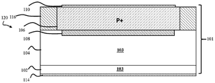
도 1은 본 발명의 일 실시예에 따른 TVS 다이오드(100)로서 도시된 단방향성 SiC TVS 다이오드를 나타낸다. TVS 다이오드(100)의 이러한 구조는 SiC 기판(101) 내에 형성된 P/N 다이오드에 상응한다. 특히, 도시된 직교 좌표계의 Z-축을 따른 다양한 영역의 두께를 비롯하여, TVS 다이오드(100)의 다양한 부분이 반드시 축척대로 그려진 것은 아니다. TVS 다이오드는 100 μm 내지 375 μm 범위의 두께를 갖는 벌크 SiC 기판에 기초하여 형성될 수 있다. 실시예들은 이와 관련하여 제한되지 않는다. 도 1의 예에서, TVS 다이오드(100)는 벌크 기판 영역(102)을 포함하는 N-형 영역(103)을 포함하며, 여기서 벌크 기판 영역(102)은 두께가 예를 들어 100 μm 내지 375 μm일 수 있다. N-형 영역(103)은 벌크 기판 영역(102) 상에 배치된, 에피택셜 SiC 층(104)을 또한 포함할 수 있다. 에피택셜 SiC 층(104)은 벌크 기판 영역(102)과 유사하거나 동일한 N-형 SiC 재료로 형성될 수 있다. 예를 들어, 벌크 기판 영역(102)은 약 3.2 eV와 같은 높은 밴드갭을 갖는 공지의 육방정계 SiC 다형성(polytype)으로 형성될 수 있다. 에피택셜 SiC 층(104)은 육방정계 다형성으로서 성장될 수 있는데, 여기서 에피택셜 SiC 층(104)과 벌크 기판 영역(102) 사이의 차이는 N-형 도펀트의 수준이다. 다른 실시예에서, 에피택셜 SiC 층(104)은 하기에 추가로 논의되는 바와 같이 생략될 수 있다. 다양한 실시예에서, 에피택셜 SiC 층(104)의 두께는 TVS 다이오드(100)의 전기적 특성을 조정하도록 조정될 수 있으며, 전형적인 두께 범위는 1 μm 내지 10 μm이다. 실시예들은 이와 관련하여 제한되지 않는다. 1 shows a unidirectional SiC TVS diode shown as a
TVS 다이오드(100)는 에피택셜 SiC 층(104)의 상부 부분에 형성된 P-형 영역(106)을 추가로 포함한다. P-형 영역(106)은 상부 표면(105)의 선택 부분을 점유하도록 마스킹 접근법에 의해 형성될 수 있으며, SiC 기판(101) 내로 수 마이크로미터 연장될 수 있다. TVS 다이오드(100)는 주입된 N-형 층(108)을 추가로 포함할 수 있으며, 주입된 N-형 층은 에피택셜 SiC 층 내에서 P-형 영역 밑에 배치되고, 주입된 N-형 층은 제2 도펀트 수준보다 큰 제3 도펀트 수준을 포함한다.The
TVS 다이오드(100)는 P-형 영역(106) 상에 배치된 애노드 접점(110), 및 N-형 영역(103)과 접촉하여 SiC 기판(101)의 배면 표면(112) 상에 배치된 배면 접점(114)을 추가로 포함할 수 있다.The
도 1에 도시된 바와 같이, P-형 영역(106)은 하부 표면(107)을 포함하고, 하부 표면(107)은 제1 단부(109)와 제2 단부(111) 사이의 제1 거리(D1)만큼 연장된다. 하부 표면(107)은 P-형 영역(106)과 N-형 영역(103) 사이의 P/N 접합부를 형성하는 역할을 할 수 있다. TVS 다이오드(100)의 항복 전압은 P-형 영역(106)과 주입된 N-형 층(108) 사이에 형성된 P-N 다이오드의 항복 전압에 의해 한정된다. 다양한 구현예에서, P-형 영역(106)의 도핑 농도는 고정될 수 있으나, 항복 전압은 N-형 층(108)을 형성하기 위해 주입 용량, 및 따라서 주입된 N-형 층(108)의 도핑 농도를 변화시킴으로써 조절될 수 있다.As shown in FIG. 1, the P-shaped
배경으로서, P-N 접합 다이오드의 항복 전압은 P-N 접합부를 가로지르는 전계가 임계 항복 전계(critical breakdown field)를 초과할 때 발생한다. P-N 접합부를 가로지르는 전계는 P-형 영역 및 N-형 영역의 도핑 농도에 의해 결정된다. TVS 다이오드(100)에서, 항복 전압은 P-형 영역(106) 및 주입된 N-형 층(108)의 도핑 농도에 의해 결정될 수 있다. 주어진 P 영역 도핑 농도에 대해, 주입된 N-형 층(108)의 도핑 농도가 증가함에 따라, TVS 다이오드의 항복 전압은 저하된다. 에피택셜 SiC 층(104)의 도핑 농도는 주입된 N-형 층(108)의 도핑 농도보다 낮다. 그 결과, 에피택셜 SiC 층(104)은 저전압 TVS 다이오드 구조체의 항복 전압에 영향을 주지 않는다.As a background, the breakdown voltage of the P-N junction diode occurs when the electric field across the P-N junction exceeds the critical breakdown field. The electric field across the P-N junction is determined by the doping concentration of the P-type region and the N-type region. In the
특히, N-주입된 영역의 도핑 농도가 N-기판 영역의 도핑 농도보다 클 필요가 있는, 낮은 항복 전압을 갖는 TVS 다이오드 구조체의 경우, N-형 에피택셜 영역을 갖지 않는 웨이퍼(기판) 상에 TVS 다이오드가 제조될 수 있다. 이러한 후자의 접근법은 저전압 TVS 다이오드 구조체의 제조 비용을 낮추는 데 유리할 수 있다.In particular, for a TVS diode structure having a low breakdown voltage, where the doping concentration of the N-injected region needs to be greater than the doping concentration of the N-substrate region, on a wafer (substrate) having no N-type epitaxial region TVS diodes can be manufactured. This latter approach may be advantageous in lowering the manufacturing cost of low voltage TVS diode structures.
적절한 디바이스 항복(device breakdown)을 보장하기 위해, 주입된 N-형 층(108)은 하부 표면(107) 전체를 따라 연장되지 않을 수 있다. 도 1의 예에서, 주입된 N-형 층(108)은 하부 표면(107)을 따라, 제1 거리(D1)보다 작은 제2 거리(D2)만큼 연장된다. 특히, 주입된 N-형 층(108)은 제1 단부(109) 및 제2 단부(111)로부터 오프셋(offset)된다.To ensure proper device breakdown, the implanted N-
다양한 실시예에서, 벌크 기판 영역(102)의 도핑 농도는 대략 1018 cm-3이며, 에피택셜 SiC 층(104)의 도핑 농도는 1014 내지 1017 cm-3의 범위이다.In various embodiments, the doping concentration of the
에피택셜 SiC 층(104)의 도핑 농도는, P-형 영역(106)과 에피택셜 SiC 층 사이에 형성된 P-N 다이오드의 항복 전압이 P-형 영역(106)과 주입된 N-형 층(108) 사이에 형성된 P-N 다이오드보다 높도록 선택될 수 있다. P-형 영역(106)은, 애노드 접점(110)으로 나타내어지는 바와 같은, 옴 금속화(ohmic metallization)를 사용하여 접촉될 수 있다. 다양한 실시예들에서, 금속화 방식은 니켈(Ni) 또는 티타늄(Ti) 기반 접점을 포함할 수 있다. 일 예에서, N-형 영역(103)은 Ni 접점을 사용하여 SiC 기판(102)의 표면(112) 상에 접촉될 수 있다.The doping concentration of the
30 V의 항복 전압을 갖는 저전압 SiC TVS를 구현하기 위한 일부 실시예에서, 예를 들어, P-형 영역(106)의 피크 도핑 농도는 1020 cm-3 정도일 수 있다. 주입된 N-형 층(108)의 도핑 농도는 1018 cm-3 정도일 수 있다. TVS 다이오드(100)의 적절한 작동을 위해, 에피택셜 SiC 층(104)의 도핑 농도는 주입된 N-형 층(108)의 도핑 농도보다 낮도록 조정된다. 예를 들어, 에피택셜 SiC 층(104)의 도핑 농도는 1016 cm-3 정도일 수 있다.In some embodiments for implementing a low voltage SiC TVS with a breakdown voltage of 30 V, for example, the peak doping concentration of the P-
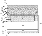
이제 도 2를 참조하면, 본 발명의 추가적인 실시예에 따라 배열된 TVS 다이오드(120)의 일 실시예가 도시되어 있다. TVS 다이오드(120)는 TVS 다이오드(100)의 동일 구성요소들을 공유할 수 있는데, JTE 영역(116)으로 도시된 접합 종단 연장 영역(JTE 영역)이 추가된다는 차이가 있다. JTE 영역(116)은 에피택셜 SiC 층(104) 내에서 P-형 영역(106) 주위에 배치되며, 에피택셜 SiC 층(104)의 일부분과 계면 영역을 형성한다. 특히, P-형 영역(106)은 제1 p-도핑 수준을 가질 수 있고, 여기서 JTE 영역(116)은 제1 p-도핑 수준보다 작은 제2 p-도핑 수준을 갖는 P-형 도펀트로 형성된다. 본 발명의 실시예에 따르면, JTE 영역(116)은 P-형 영역(106)을 둘러싸도록 더 낮은 도핑 농도의 p-도펀트를 갖는 영역을 확립하기 위해 이온 주입 작업에 의해 형성될 수 있다. 일부 실시예에서, JTE 영역(116)의 도핑 농도는 1017 cm-3 정도이다. 이와 같이, JTE 영역(116)은 디바이스 에지에서의 표면 전계를 감소시켜 TVS 다이오드(120)가 목표값 미만에서 항복되지 않도록 보장할 수 있다.Referring now to FIG. 2 , one embodiment of a
이제 도 3을 참조하면, 본 발명의 추가의 실시예에 따른 TVS 다이오드(130)가 도시되어 있다. 도 3의 실시예는 도 2의 TVS 다이오드(120)의 특징부들과 유사한 특징부들을 공유하는데, 애노드 접점(110) 위에 배치된 장벽 금속 층(122)으로 표시된 금속 층 구조체로서 도시된 선택적인 배리어 층을 비롯한 추가적인 특징부가 TVS 다이오드(120)에는 존재하지 않는다. TVS 다이오드(130)는 필드 산화물(field oxide) 층(124)으로 도시된 필드 산화물 영역에 의해 한정되는 윈도우(window) 내에 형성된 금속화 영역(126)을 추가로 포함한다. 장벽 금속 층(122)은, 일부 실시예에 따르면, Ti, 또는 Ti와 질화티타늄(TiN)의 조합일 수 있다. 금속화 영역(126)은 일부 실시예에서 알루미늄:구리 합금 재료일 수 있으며, 특정 실시예에서 1 마이크로미터 초과, 예를 들어 4 마이크로미터의 두께를 가질 수 있다. TVS 다이오드(130)는 금속화 영역(126) 위에 배치된 패시베이션 층(128)을 추가로 포함할 수 있다. 패시베이션 층(128)을 위한 적합한 재료 시스템의 예는 포스포실리케이트 유리(PSG) 및 질화규소(SiNx)이다. 일 예에서, PSG의 두께는 500 nm일 수 있으며, SiNx의 두께는 850 nm일 수 있다. 실시예들은 이와 관련하여 제한되지 않는다. 도 3에 도시된 바와 같이, 폴리이미드와 같은 중합체 층(132)이 패시베이션 층(128) 위에 제공된다. 이어서, 중합체 층(132) 및 패시베이션 층(128)에는 TVS 다이오드(130) 및 조립체와의 전기적 접촉을 가능하게 하기 위한 개방부(도시되지 않음)가 제공될 수 있다. 니켈/금 또는 니켈/팔라듐/금을 함유하는 납땜 가능한 전면 금속화 층이 또한 금속화 영역(126) 위에 존재할 수 있다. 특히, 도 1 및 도 2의 실시예에서, TVS 다이오드와의 접촉을 제공하기 위해, 유사한 금속화 및 부동태화 방식 또는 다른 공지의 적합한 금속화 방식이 각각의 TVS 다이오드에 부가될 수 있다.Referring now to FIG. 3 , a
에피택셜 SiC 층(104)이 제공되는 상기에 논의된 실시예들에서, 다양한 영역들의 도핑 수준 및 두께는, 20 V를 초과하지만 650 V 미만인 목표 항복 전압을 생성하도록 용이하게 조정될 수 있다. 특정 실시예에서, 에피택셜 SiC 층(104) 영역의 도핑 농도는 주입된 N-형 층(108)의 도핑 농도보다 작다. 주입된 N-형 층(108)의 도핑 농도 및 두께는 각각 1016 cm-3 초과 및 10 μm 미만일 수 있다. P-형 영역(106)의 도핑 수준은 1018 cm-3 초과일 수 있으며, 특정 실시예에서 대략 1020 cm-3일 수 있다. 마찬가지로, 주입된 N-형 층의 도핑 수준은 1018 cm-3일 수 있으며, 여기서 정확한 값은 SiC P-N 다이오드의 목표 항복 전압에 의해 결정된다. 더욱이, 일부 실시예에 따르면, 벌크 기판 영역(102)의 두께는 350 μm 이하일 수 있다. 특히, 주입된 N-형 층(108)은 P-형 영역(106) 내에 있도록 형성될 수 있다. 일 구현예에서, 주입된 N-형 층(108)은 P-형 영역(106)의 에지로부터 10 μm만큼 이격된다. 다른 실시예에서, 주입된 N-형 층(108)은 P-형 영역(106)의 에지로부터 5 μm만큼 이격될 수 있다. 실시예들은 이와 관련하여 제한되지 않는다. 일반적으로, N-형 층은 P-형 영역(106)의 에지로부터 이격되어 N-형 주입된 층(108)이 P-형 영역(106) 내에 수용되도록 보장한다.In the embodiments discussed above where the
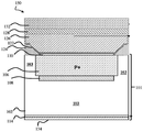
이제 도 4를 참조하면, 본 발명의 추가의 실시예에 따른 TVS 다이오드(140)가 도시되어 있다. 도 4의 실시예는 도 3의 TVS 다이오드(130)의 특징부들과 유사한 특징부들을 공유하지만, TVS 다이오드(140)는 JTE 영역(116)을 포함하지 않는다.Referring now to FIG. 4 , a
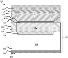
이제 도 5를 참조하면, 본 발명의 추가의 실시예에 따른 TVS 다이오드(150)가 도시되어 있다. 도 4의 실시예는 도 4의 TVS 다이오드(140)의 특징부들과 유사한 특징부들을 공유하지만, TVS 다이오드(150)는 SiC 에피택셜 층(104)을 포함하지 않는다. 주입된 N-형 층(108)의 도핑 농도는 SiC 에피택셜 층(104)의 부재를 고려하도록 조정될 수 있다.Referring now to FIG. 5 , a
일 예로서, 벌크 기판 영역(102)에서 0.02 Ohm-cm의 저항률을 갖는 기판의 경우, N-형 도펀트의 상응하는 도펀트 농도는 대략 1.6 × 1018 cm-3이며, 따라서, 주입된 N-형 층(108)의 도핑 농도는 1.6 × 1018 cm-3 초과일 수 있다. 일부 실시예에 따르면, 도 5의 구조를 갖는 생성된 P/N 다이오드는 20 V 초과 100 V 미만의 항복 전압을 나타낼 수 있다.As an example, for a substrate having a resistivity of 0.02 Ohm-cm in the
이제 도 6을 참조하면, 본 발명의 추가의 실시예에 따른 TVS 다이오드(160)가 도시되어 있다. 도 6의 실시예는 도 5의 TVS 다이오드(150)의 특징부들과 유사한 특징부들을 공유하며, 앞서 논의된 JTE 영역(116)이 추가된 것이다. JTE 영역(116)에 대한 도핑 공정은 벌크 기판 영역(102)의 도핑 농도뿐만 아니라 P-형 영역(106)의 도핑 농도를 고려하여 조정될 수 있다. 특히, JTE 영역(116) 내의 P-형 도펀트의 농도는 P-형 영역(106) 내의 P-형 도펀트의 농도보다 작게 설정된다. 게다가, JTE 영역(116)이 이온 주입에 의해 형성될 수 있기 때문에, JTE 영역(116)을 형성하기 위한 주입 스케줄은 벌크 기판 영역(102) 내의 N-형 도펀트의 기존의 도핑 농도를 보상하도록 조정될 수 있다. 벌크 기판 영역(102) 내의 N-형 도펀트의 농도가 1.6 × 1018 cm-3과 같이 비교적 높기 때문에, JTE 영역(116)을 형성하는 데 사용되는 P-형 이온의 주입 용량은 대략 1017 cm-3의 순 P-형 도펀트 농도를 산출하도록 조정될 것이다. 따라서, P-형 이온의 주입은 벌크 기판 영역(102) 내의 N-형 도펀트 내의 활성 N-형 도펀트 농도를 보상하기 위해 1.6 × 10¹⁸ 초과의 총 도펀트 농도를 도입할 수 있다. 비교로서, SiC 에피택셜 층(104) 내로의 주입에 의해 JTE 영역 형성이 발생하는 도 2의 실시예에서, N-형 도펀트 농도는 P-형 이온이 주입되는 SiC 기판(101)의 영역에서 1016 cm-3 정도일 수 있다. 따라서, JTE 영역(116)에서 대략 1017 cm-3의 순 P-형 도펀트 농도를 산출하기 위해, 도 2의 실시예에서 P-형 종들의 총 도펀트 농도는 1016 cm-3의 N-형 도펀트 농도를 보상하기 위해 1.5 × 1017 cm-3과 같이 단지 약간 더 높을 수 있다.Referring now to FIG. 6 , a
이제 도 7a 내지 도 7j를 참조하면, 본 발명의 실시예에 따른 TVS 다이오드를 조립하기 위한 공정 흐름이 도시되어 있다. 이 공정 흐름은 전술한 TVS 다이오드(130)의 형성에 특히 적용될 수 있다. 도 7a에서, 도시된 바와 같이, 벌크 기판 영역(102), 및 SiC 에피택셜 층(104)을 포함하는 SiC 기판(101)이 제공된다.Referring now to FIGS . 7A- 7J , a process flow for assembling a TVS diode according to an embodiment of the invention is shown. This process flow can be particularly applied to the formation of the
도 7b에서, 제1 주입 마스크(180)가 제공되며, 여기서 제1 주입 마스크는 제1 개구(181)를 형성하여 N-형 영역(103)의 제1 부분, 및 특히 SiC 에피택셜 층(104)의 제1 부분을 노출시킨다. 도 7b의 단계에서, P-형 도펀트 종의 주입이 발생하였고 이는 P-형 영역(106)의 형성으로 이어진다. P-형 도펀트 이온을 주입하기 위한 이온 에너지는 P-형 영역(106)의 목표 두께, 예를 들어 수 마이크로미터 깊이에 대해 맞춰질 수 있다. P-형 영역(106)의 위치 및 측방향 크기는 제1 개구(181)에 의해 한정된다. 제1 주입 마스크(180)에 적합한 재료는 산화규소이며, 이 산화규소의 두께는 제1 주입 마스크(180) 아래의 에피택셜 SiC 층(104) 내로의 주입을 방지하기 위해 이온을 함유하도록 맞춰질 수 있다.In FIG. 7B , a
도 7c의 단계에서, 제1 주입 마스크(180)가 제거될 수 있고, 제2 주입 마스크(182)가 제공될 수 있으며, 여기서 제2 주입 마스크(182)는 제2 개구(183)를 형성하여 N-형 영역(103)의 제2 부분, 및 특히 SiC 에피택셜 층(104)의 제2 부분을 노출시킨다. 도 7c의 단계에서, N-형 도펀트 종의 주입이 발생하였고 이는 주입된 N-형 영역(108)의 형성으로 이어진다. N-형 도펀트 이온을 주입하기 위한 이온 에너지는 상부 표면(105) 아래로 수 마이크로미터와 같은, 주입된 N-형 영역(108)의 목표 깊이 및 두께에 대해 맞춰질 수 있다. P-형 영역(106)의 위치 및 측방향 크기는 제2 개구(183)에 의해 한정된다. 제2 주입 마스크(182)에 적합한 재료는 산화규소이며, 산화규소의 두께는 제2 주입 마스크(182) 아래의 에피택셜 SiC 층(104) 내로의 주입을 방지하기 위해 이온을 함유하도록 맞춰질 수 있다. 특히, 제2 개구(183)는 제1 개구(181)의 치수(D1)보다 작은 치수(D2)로 배열될 수 있다. 제2 개구(183)는 또한 X-축 및 Y-축 둘 모두를 따라 제1 개구(181) 내에 속하도록 정렬될 수 있으므로, 주입된 N-형 층(108)은 X-Y 평면에서 P-형 영역(106)을 넘어 연장되지 않는다. In the step of FIG. 7C , the
도 7d의 단계에서, 제2 주입 마스크(182)가 제거될 수 있고, 제3 주입 마스크(184)가 제공될 수 있으며, 여기서 제3 주입 마스크(184)는 JTE 마스크로서 작용하고 제3 개구(185)를 형성하여 N-형 영역(103)의 제3 부분, 및 특히 SiC 에피택셜 층(104)의 제3 부분을 노출시킨다. 도 7d의 단계에서, P-형 도펀트 종의 주입이 발생하였고, 이는 JTE 영역(116)의 형성으로 이어진다. 제3 주입 마스크(184)는 도시된 바와 같이 P-형 영역(106)을 덮도록 정렬될 수 있다. P-형 도펀트 이온을 주입하기 위한 이온 에너지는 상부 표면(105) 아래로 수 마이크로미터와 같은 JTE 영역(116)의 목표 깊이에 대해 맞춰질 수 있다. JTE 영역(116)의 위치 및 측방향 크기는 개구(185)에 의해 한정된다. 제3 주입 마스크(184)에 적합한 재료는 산화규소이며, 산화규소의 두께는 제3 주입 마스크(184) 아래의 에피택셜 SiC 층(104) 내로의 주입을 방지하기 위해 이온을 함유하도록 맞춰질 수 있다. 특히, 도 7d의 단계 후에, 활성화 어닐링 절차가 수행되어, 도 7b 내지 도 7d의 절차에 의해 형성된 다양한 영역에서 N-도펀트 및 P-도펀트를 활성화시킬 수 있다.In the step of FIG. 7D , the
다양한 비제한적인 실시예에서, P-형 영역(106)의 깊이(DP)는 0.5 μm 내지 2 μm일 수 있으며, P-형 영역(106)의 폭(WP)은 수백 마이크로미터 내지 수 밀리미터와 같이 다이오드 응용에 따라 변할 수 있다. 더 큰 P+ 폭은 더 큰 전체 TVS 다이오드 다이 크기를 초래하여, TVS가 일부 응용에 필요한 더 높은 출력 용량을 갖는 것을 용이하게 할 것이다. 다양한 다른 비제한적인 실시예에서, 폭(WN)을 갖는 주입된 N-형 층(108)은 P-형 영역(106)의 에지로부터 5 μm 내지 10 μm만큼 오프셋될 수 있다(오프셋을 보여주는, 점선 영역 참조). 오프셋은, 항복 전압이 제어되고 P+ 접합 코너들에서 디바이스의 조기 항복이 없도록 보장한다.In various non-limiting embodiments, the depth D P of the P -
도 7e에 도시된 후속 단계에서, 필드 산화물 층(124)에 의해 나타내어지는 바와 같은 산화물 층이 침착되었다. 필드 산화물은 공지된 치밀화(densification) 어닐링 및 패턴화를 거쳐, 도시된 바와 같이 P-형 영역(106) 위에 개구(185)를 형성할 수 있다. In the subsequent step shown in FIG. 7E , an oxide layer, as represented by
도 7f에 도시된 후속 단계에서, 애노드 접점(110) 및 배면 접점(114)이 침착 및 어닐링되어 TVS 다이오드의 반도체 영역과의 옴 접점을 형성하였다.In the subsequent steps illustrated in FIG. 7F , the
도 7g에 도시된 후속 단계에서, 장벽 금속 층(122) 및 금속화 영역(126)이 침착, 패턴화 및 에칭되어, 도시된 접점 구조를 형성하였다. 도 7h에 도시된 후속 단계에서, 패시베이션 층(128)이 침착, 패턴화, 및 에칭되어, 도시된 구조를 형성하였다. 도 7i에 도시된 후속 단계에서, 중합체 층(132)이 침착, 현상 및 경화되었다. 도 7j에 도시된 후속 단계에서, 도시된 바와 같이 최종 금속 층(134)이 배면 표면 상에 침착되었다. In the subsequent steps shown in FIG. 7G ,
다양한 추가적인 실시예에서, 임의의 전술한 TVS 디바이스가 하기의 사양에 따라 제조될 수 있다: A) P-형 영역(106)의 순 도핑 농도: 1018 내지 1020 cm-3; B) P-형 JTE 영역(116)의 순 도핑 농도: 1 × 10¹⁷ 내지 5 × 1017 cm-3; C) N-에피택셜 층의 순 도핑 농도: 1 × 1014 cm-3 내지 5 × 1017 cm-3; 및 D) 주입된 N-영역의 순 도핑 농도: 1 × 10¹⁶ 내지 5 × 1018 cm- 3. 이러한 범위의 도핑 농도는 15 V 내지 600 V 범위의 항복 전압을 갖는 디바이스를 산출할 것이다.In various additional embodiments, any of the aforementioned TVS devices can be manufactured according to the following specifications: A) Net doping concentration of P-type region 106: 10 18 to 10 20 cm -3 ; B) Net doping concentration of P-type JTE region 116: 1 × 10 17 to 5 × 10 17 cm -3 ; C) Net doping concentration of N-epitaxial layer: 1 × 10 14 cm -3 to 5 × 10 17 cm -3 ; And D) the net doping concentration of the implanted N- regions: 1 × 10 16 to 5 × 10 18 cm - 3. Doping concentrations in this range will yield devices with breakdown voltages ranging from 15 V to 600 V.
요약하면, 본 실시예들은 Si-기반 TVS 디바이스에 비해 다양한 이점을 제공한다. 본 실시예의 SiC-기반 TVS 다이오드는, 더 높은 전압을 위한 Si 다이오드의 경우에서와 같이 복수의 다이를 직렬로 접속시켜야 할 필요성을 피하면서, 반도체 다이에서의 항복 전압을 15 V 초과 600 V 이하와 같은 전압 범위에 걸쳐 설계하는 능력을 제공한다. 본 실시예는 Si TVS 다이오드에 비해 누설이 감소된, 고온 작동을 위한 더 강건한 다이오드를 또한 제공한다.In summary, the present embodiments provide various advantages over Si-based TVS devices. The SiC-based TVS diode of this embodiment avoids the need to connect a plurality of dies in series, as in the case of Si diodes for higher voltages, with breakdown voltages in the semiconductor die greater than 15 V and less than 600 V. It provides the ability to design over the same voltage range. This embodiment also provides a more robust diode for high temperature operation with reduced leakage compared to Si TVS diodes.
도 8은 본 발명의 실시예에 따른 예시적인 공정 흐름(800)을 나타낸다. 블록(802)에서는, SiC 기판에 N-형 영역이 제공된다. N-형 영역은 제1 도핑 수준을 갖는 벌크 기판 영역, 및 제1 도핑 수준보다 작은 제2 도핑 수준을 갖는 에피택셜 SiC 층을 포함할 수 있다. 8 shows an
블록(804)에서, P-형 이온을 주입하여 N-형 영역의 제1 표면으로부터 연장되는 P-형 영역을 형성하는 작업이 수행된다. 블록(806)에서, P-형 영역 밑에 N-형 이온을 주입함으로써 주입된 N-형 층이 형성된다. 그러므로, 주입된 N-형 층은 P-형 영역과 N-형 영역 사이에 배치될 수 있다.In
TVS 다이오드와 관련된 디바이스 및 방법이 소정의 실시예를 참조하여 기재되었지만, 본 출원의 청구범위의 사상 및 범주로부터 벗어남이 없이 다양한 변화가 이루어질 수 있으며 등가물이 대체될 수 있음이 당업자에 의해 이해될 것이다. 청구범위의 범주로부터 벗어남이 없이 특정 상황 또는 재료를 상기에 개시된 교시에 적응시키기 위해 다른 수정이 이루어질 수 있다. 따라서, 청구범위는 개시된 특정 실시예들 중 어느 하나로 한정되는 것이 아니라, 청구범위의 범주 내에 속하는 임의의 실시예들로 한정되는 것으로 해석되어야 한다.Although devices and methods related to TVS diodes have been described with reference to certain embodiments, it will be understood by those skilled in the art that various changes may be made and equivalents may be substituted without departing from the spirit and scope of the claims of the present application. . Other modifications can be made to adapt a particular situation or material to the teachings disclosed above without departing from the scope of the claims. Accordingly, the claims should not be limited to any of the specific embodiments disclosed, but should be construed as limited to any embodiment falling within the scope of the claims.
Claims (19)
상기 SiC 기판 내에 형성된 N-형 영역;
상기 N-형 영역의 상부 부분에 형성된 P-형 영역; 및
상기 P-형 영역과 상기 N-형 영역 사이에 배치된 주입된(implanted) N-형 층
을 포함하는, 디바이스.
PN diode formed in the SiC substrate (substrate),
An N-type region formed in the SiC substrate;
A P-type region formed in an upper portion of the N-type region; And
An implanted N-type layer disposed between the P-type region and the N-type region
Including, the device.
제1 도핑 수준을 갖는 벌크 기판 영역; 및
상기 벌크 기판 영역과 상기 주입된 N-형 층 사이에 배치되며 상기 제1 도핑 수준보다 작은 제2 도핑 수준을 갖는 에피택셜 SiC 층
을 포함하는, 디바이스.
The method of claim 1, wherein the N-type region
A bulk substrate region having a first doping level; And
An epitaxial SiC layer disposed between the bulk substrate region and the implanted N-type layer and having a second doping level less than the first doping level
Including, the device.
3. The junction termination extension (JTE) region of claim 2, wherein a junction termination extension (JTE) region is disposed within the epitaxial SiC layer around the P-type region and forms an interface region with a portion of the epitaxial SiC layer. Device, wherein the P-type region comprises a first p-doped level, and the JTE region comprises a p-type dopant having a second p-doped level less than the first p-doped level .
The P-type region of claim 1, further comprising a junction termination extension region (JTE region) disposed around the P-type region and forming an interface region with the N-type region, wherein the P-type region comprises a first p-type region. A device comprising a doping level, the JTE region comprising a p-type dopant having a second p-doping level less than the first p-doping level.
The P-type region of claim 1, wherein the P-type region includes a lower surface, the lower surface extends a first distance between the first end and the second end, and the implanted N-type layer covers the lower surface. The device thus extends by a second distance less than the first distance and is offset from the first end and the second end.
The device of claim 4, wherein the P-type region comprises a bottom surface, and the implanted N-type layer extends along the bottom surface and is offset from the junction termination extension region.
The device of claim 1 comprising a breakdown voltage greater than 20 V and less than 650 V.
The device of claim 1, wherein the N-type region comprises a bulk substrate region, and the implanted N-type layer is formed in the bulk substrate region.
10. The device of claim 8, wherein the PN diode comprises a breakdown voltage greater than 20 V and less than 100 V.
상기 P-형 영역 상에 배치된 애노드 접점; 및
상기 N-형 영역과 접촉하여 상기 SiC 기판의 배면 표면 상에 배치된 배면 접점
을 추가로 포함하는, 디바이스.
According to claim 1,
An anode contact disposed on the P-type region; And
A back contact disposed on the back surface of the SiC substrate in contact with the N-type region
The device further comprising a.
상기 P-형 영역 위에서 윈도우(window)를 형성하는 필드 산화물(field oxide) 영역;
상기 애노드 접점과 접촉하여 배치된 금속 층 구조체;
상기 금속 층 구조체 위에 배치된 패시베이션 층; 및
상기 금속 층 구조체 위에 배치된 중합체 층
을 추가로 포함하며, 상기 중합체 층 및 상기 금속 층 구조체는 상기 금속 층 구조체와 접촉하기 위한 개방부를 형성하는, 디바이스.
The method of claim 10,
A field oxide region forming a window on the P-type region;
A metal layer structure disposed in contact with the anode contact;
A passivation layer disposed over the metal layer structure; And
A polymer layer disposed over the metal layer structure
And further comprising, the polymer layer and the metal layer structure forming an opening for contacting the metal layer structure.
SiC 기판에 N-형 영역을 제공하는 단계;
P-형 이온을 주입하여 상기 N-형 영역의 제1 표면으로부터 연장되는 P-형 영역을 형성하는 단계; 및
상기 P-형 영역 밑에 N-형 이온을 주입함으로써 주입된 N-형 층을 형성하는 단계
를 포함하며, 상기 주입된 N-형 층은 상기 P-형 영역과 상기 N-형 영역 사이에 배치되는, 방법.
As a method of forming a SiC TVS diode,
Providing an N-type region in the SiC substrate;
Implanting P-type ions to form a P-type region extending from the first surface of the N-type region; And
Forming an implanted N-type layer by implanting N-type ions under the P-type region
And wherein the implanted N-type layer is disposed between the P-type region and the N-type region.
벌크 기판 영역을 포함하는 SiC 기판을 제공하는 단계로서, 상기 벌크 기판 영역은 제1 도핑 수준의 N-형 도펀트를 갖는, 상기 단계; 및
상기 벌크 기판 영역 상에 에피택셜 SiC 층을 성장시키는 단계로서, 상기 에피택셜 SiC 층은 N-형 도펀트를 포함하며 상기 제1 도핑 수준보다 작은 제2 도핑 수준을 갖는, 상기 단계
를 포함하는, 방법.
The method of claim 12, wherein providing the N-type region comprises:
Providing a SiC substrate comprising a bulk substrate region, the bulk substrate region having an N-type dopant at a first doping level; And
Growing an epitaxial SiC layer on the bulk substrate region, the epitaxial SiC layer comprising an N-type dopant and having a second doping level less than the first doping level
How to include.
14. The method of claim 13, further comprising forming a junction termination extension region (JTE region) around the P-type region in the epitaxial SiC layer by injecting a P-type dopant, wherein the P-type region Method comprising a first p-doped level, and the P-type dopant in the JTE region comprises a second p-doped level less than the first p-doped level.
13. The method of claim 12, further comprising forming a junction termination extension region (JTE region) in the N-type region by injecting a P-type dopant around the P-type region, wherein the P-type region Method comprising a first p-doped level, wherein the P-type dopant has a second p-doped level less than the first p-doped level.
13. The method of claim 12, wherein forming the implanted N-type layer comprises implanting the N-type ion through a first implantation mask, and forming the P-type region comprises a second implantation. And implanting the P-type ion through a mask, wherein the second implantation mask is arranged such that the P-type region extends by a first distance between the first end and the second end, and the first implantation. The mask is arranged such that the implanted N-type layer extends a second distance less than the first distance and is offset from the first end and the second end.
16. The method of claim 15, wherein forming the implanted N-type layer comprises implanting the N-type ion through a first implantation mask, and forming the JTE region comprises: And implanting a P-type ion, wherein the JTE mask is arranged such that the P-type region extends by a first distance between the first end and the second end, and the first implantation mask is the implanted N A method in which a mold layer is arranged to extend by a second distance less than the first distance and offset from the first end and the second end.
제1 도펀트 수준을 갖는 N-형 SiC를 포함하는 벌크 기판 영역;
상기 벌크 기판 영역 상에 배치되며, 제2 도펀트 수준을 갖는 N-형 SiC 재료를 포함하는 에피택셜 SiC 층;
상기 에피택셜 SiC 층의 상부 부분에 형성된 P-형 영역; 및
주입된 N-형 층
을 포함하며, 상기 주입된 N-형 층은 상기 에피택셜 SiC 층 내에서 상기 P-형 영역 밑에 배치되고, 상기 주입된 N-형 층은 상기 제2 도펀트 수준보다 큰 제3 도펀트 수준을 포함하는, SiC TVS 디바이스.
As a SiC TVS device,
A bulk substrate region comprising N-type SiC having a first dopant level;
An epitaxial SiC layer disposed on the bulk substrate region and comprising an N-type SiC material having a second dopant level;
A P-type region formed in an upper portion of the epitaxial SiC layer; And
Injected N-type layer
, Wherein the implanted N-type layer is disposed under the P-type region within the epitaxial SiC layer, and the implanted N-type layer comprises a third dopant level greater than the second dopant level , SiC TVS devices.
Priority Applications (1)
| Application Number | Priority Date | Filing Date | Title |
|---|---|---|---|
| KR1020240067054A KR102910198B1 (en) | 2018-09-05 | 2024-05-23 | Structure and method for sic based protection device |
Applications Claiming Priority (2)
| Application Number | Priority Date | Filing Date | Title |
|---|---|---|---|
| US16/121,916 US10910501B2 (en) | 2018-09-05 | 2018-09-05 | Stucture and method for SIC based protection device |
| US16/121,916 | 2018-09-05 |
Related Child Applications (1)
| Application Number | Title | Priority Date | Filing Date |
|---|---|---|---|
| KR1020240067054A Division KR102910198B1 (en) | 2018-09-05 | 2024-05-23 | Structure and method for sic based protection device |
Publications (2)
| Publication Number | Publication Date |
|---|---|
| KR20200027902A true KR20200027902A (en) | 2020-03-13 |
| KR102670357B1 KR102670357B1 (en) | 2024-05-30 |
Family
ID=67875262
Family Applications (2)
| Application Number | Title | Priority Date | Filing Date |
|---|---|---|---|
| KR1020190109505A Active KR102670357B1 (en) | 2018-09-05 | 2019-09-04 | Structure and method for sic based protection device |
| KR1020240067054A Active KR102910198B1 (en) | 2018-09-05 | 2024-05-23 | Structure and method for sic based protection device |
Family Applications After (1)
| Application Number | Title | Priority Date | Filing Date |
|---|---|---|---|
| KR1020240067054A Active KR102910198B1 (en) | 2018-09-05 | 2024-05-23 | Structure and method for sic based protection device |
Country Status (5)
| Country | Link |
|---|---|
| US (1) | US10910501B2 (en) |
| EP (2) | EP3621121A1 (en) |
| KR (2) | KR102670357B1 (en) |
| CN (1) | CN110880538B (en) |
| TW (1) | TWI809185B (en) |
Families Citing this family (2)
| Publication number | Priority date | Publication date | Assignee | Title |
|---|---|---|---|---|
| CN112928168B (en) | 2019-12-06 | 2025-06-27 | 力特半导体(无锡)有限公司 | TVS diodes and components with asymmetric breakdown voltage |
| TWI862120B (en) * | 2023-08-30 | 2024-11-11 | 台亞半導體股份有限公司 | Wide-band-gap diode and manufacturing method thereof |
Citations (2)
| Publication number | Priority date | Publication date | Assignee | Title |
|---|---|---|---|---|
| US20040070005A1 (en) * | 2002-04-30 | 2004-04-15 | Zarlink Semiconductor Inc. | Compact high voltage ESD protection diode |
| US20130334695A1 (en) * | 2012-06-19 | 2013-12-19 | Nxp B.V. | Electronic device and method of manufacturing such device |
Family Cites Families (14)
| Publication number | Priority date | Publication date | Assignee | Title |
|---|---|---|---|---|
| NL7907680A (en) | 1979-10-18 | 1981-04-22 | Philips Nv | ZENERDIODE. |
| US20070090360A1 (en) * | 2005-10-20 | 2007-04-26 | Vishay General Semiconductors, Llc | Blanket implant diode |
| US8431958B2 (en) * | 2006-11-16 | 2013-04-30 | Alpha And Omega Semiconductor Ltd | Optimized configurations to integrate steering diodes in low capacitance transient voltage suppressor (TVS) |
| CN101383287B (en) * | 2008-09-27 | 2010-12-08 | 电子科技大学 | A method of manufacturing a vertical double-diffused metal oxide semiconductor device |
| US8445917B2 (en) * | 2009-03-20 | 2013-05-21 | Cree, Inc. | Bidirectional silicon carbide transient voltage suppression devices |
| US9048106B2 (en) * | 2012-12-13 | 2015-06-02 | Diodes Incorporated | Semiconductor diode assembly |
| US9425153B2 (en) * | 2013-04-04 | 2016-08-23 | Monolith Semiconductor Inc. | Semiconductor devices comprising getter layers and methods of making and using the same |
| US9431385B2 (en) * | 2013-08-09 | 2016-08-30 | Semiconductor Components Industries, Llc | Semiconductor component that includes a common mode filter and method of manufacturing the semiconductor component |
| US9478606B2 (en) | 2014-02-13 | 2016-10-25 | Microsemi Corporation | SiC transient voltage suppressor |
| DE102015118165A1 (en) * | 2015-10-23 | 2017-04-27 | Infineon Technologies Ag | ELECTRICAL MODULE, COMPRISING A SEMICONDUCTOR SWITCHING DEVICE AND A TERMINAL DIODE |
| JP6705155B2 (en) * | 2015-11-13 | 2020-06-03 | 富士電機株式会社 | Semiconductor device and method of manufacturing semiconductor device |
| WO2017177429A1 (en) * | 2016-04-15 | 2017-10-19 | Littelfuse Semiconductor (Wuxi) Co., Ltd. | Overvoltage protection and linear regulator device module |
| JP6855793B2 (en) * | 2016-12-28 | 2021-04-07 | 富士電機株式会社 | Semiconductor device |
| CN106847879B (en) * | 2017-01-19 | 2021-12-03 | 北京世纪金光半导体有限公司 | SiC MOSFET device with inclined channel and preparation method |
-
2018
- 2018-09-05 US US16/121,916 patent/US10910501B2/en active Active
-
2019
- 2019-09-02 TW TW108131452A patent/TWI809185B/en active
- 2019-09-03 CN CN201910831358.1A patent/CN110880538B/en active Active
- 2019-09-04 KR KR1020190109505A patent/KR102670357B1/en active Active
- 2019-09-05 EP EP19195719.0A patent/EP3621121A1/en not_active Ceased
- 2019-09-05 EP EP22176219.8A patent/EP4075517A1/en active Pending
-
2024
- 2024-05-23 KR KR1020240067054A patent/KR102910198B1/en active Active
Patent Citations (2)
| Publication number | Priority date | Publication date | Assignee | Title |
|---|---|---|---|---|
| US20040070005A1 (en) * | 2002-04-30 | 2004-04-15 | Zarlink Semiconductor Inc. | Compact high voltage ESD protection diode |
| US20130334695A1 (en) * | 2012-06-19 | 2013-12-19 | Nxp B.V. | Electronic device and method of manufacturing such device |
Also Published As
| Publication number | Publication date |
|---|---|
| KR102910198B1 (en) | 2026-01-09 |
| TWI809185B (en) | 2023-07-21 |
| US10910501B2 (en) | 2021-02-02 |
| KR102670357B1 (en) | 2024-05-30 |
| US20200075780A1 (en) | 2020-03-05 |
| EP4075517A1 (en) | 2022-10-19 |
| KR20240078639A (en) | 2024-06-04 |
| CN110880538B (en) | 2025-11-28 |
| CN110880538A (en) | 2020-03-13 |
| TW202013672A (en) | 2020-04-01 |
| EP3621121A1 (en) | 2020-03-11 |
Similar Documents
| Publication | Publication Date | Title |
|---|---|---|
| EP2183833B1 (en) | Epitaxial surge protection device | |
| US9679998B2 (en) | Bi-directional punch-through semiconductor device and manufacturing method thereof | |
| KR102910198B1 (en) | Structure and method for sic based protection device | |
| EP2183832B1 (en) | Low capacitance semiconductor device | |
| CN113646901B (en) | Schottky rectifier with surge current stability and method for manufacturing the same | |
| Lynch et al. | Design considerations for high voltage SiC power devices: An experimental investigation into channel pinching of 10kV SiC junction barrier schottky (JBS) diodes | |
| US9831327B2 (en) | Electrostatic discharge protection devices and methods of forming the same | |
| KR101800331B1 (en) | Zener diode having a polysilicon layer for improved reverse surge capability and decreased leakage current | |
| US7238553B1 (en) | Method of forming a high-voltage silicon controlled rectifier structure with improved punch through resistance | |
| CN107293533A (en) | Transient Voltage Suppressor and its manufacture method | |
| CN107301996B (en) | Transient voltage suppressor and method of manufacturing the same | |
| EP4340045A1 (en) | Bidirectional asymmetric transient voltage suppressor device | |
| CN219303673U (en) | Unidirectional high-voltage punch-through transient voltage suppression device | |
| CN219040487U (en) | Asymmetric bidirectional transient voltage suppression device | |
| CN113284938B (en) | Semiconductor device and method for manufacturing semiconductor device | |
| CN107301997B (en) | Transient voltage suppressor and method of manufacturing same | |
| CN117917780A (en) | Unidirectional high voltage punch-through TVS diode and manufacturing method thereof |
Legal Events
| Date | Code | Title | Description |
|---|---|---|---|
| PA0109 | Patent application |
St.27 status event code: A-0-1-A10-A12-nap-PA0109 |
|
| R18-X000 | Changes to party contact information recorded |
St.27 status event code: A-3-3-R10-R18-oth-X000 |
|
| P11-X000 | Amendment of application requested |
St.27 status event code: A-2-2-P10-P11-nap-X000 |
|
| P13-X000 | Application amended |
St.27 status event code: A-2-2-P10-P13-nap-X000 |
|
| PG1501 | Laying open of application |
St.27 status event code: A-1-1-Q10-Q12-nap-PG1501 |
|
| A201 | Request for examination | ||
| PA0201 | Request for examination |
St.27 status event code: A-1-2-D10-D11-exm-PA0201 |
|
| D13-X000 | Search requested |
St.27 status event code: A-1-2-D10-D13-srh-X000 |
|
| D14-X000 | Search report completed |
St.27 status event code: A-1-2-D10-D14-srh-X000 |
|
| E902 | Notification of reason for refusal | ||
| PE0902 | Notice of grounds for rejection |
St.27 status event code: A-1-2-D10-D21-exm-PE0902 |
|
| AMND | Amendment | ||
| E13-X000 | Pre-grant limitation requested |
St.27 status event code: A-2-3-E10-E13-lim-X000 |
|
| P11-X000 | Amendment of application requested |
St.27 status event code: A-2-2-P10-P11-nap-X000 |
|
| P13-X000 | Application amended |
St.27 status event code: A-2-2-P10-P13-nap-X000 |
|
| E601 | Decision to refuse application | ||
| PE0601 | Decision on rejection of patent |
St.27 status event code: N-2-6-B10-B15-exm-PE0601 |
|
| AMND | Amendment | ||
| E13-X000 | Pre-grant limitation requested |
St.27 status event code: A-2-3-E10-E13-lim-X000 |
|
| P11-X000 | Amendment of application requested |
St.27 status event code: A-2-2-P10-P11-nap-X000 |
|
| P13-X000 | Application amended |
St.27 status event code: A-2-2-P10-P13-nap-X000 |
|
| PX0901 | Re-examination |
St.27 status event code: A-2-3-E10-E12-rex-PX0901 |
|
| PX0701 | Decision of registration after re-examination |
St.27 status event code: A-3-4-F10-F13-rex-PX0701 |
|
| X701 | Decision to grant (after re-examination) | ||
| PA0107 | Divisional application |
St.27 status event code: A-0-1-A10-A18-div-PA0107 St.27 status event code: A-0-1-A10-A16-div-PA0107 |
|
| PR0701 | Registration of establishment |
St.27 status event code: A-2-4-F10-F11-exm-PR0701 |
|
| PR1002 | Payment of registration fee |
St.27 status event code: A-2-2-U10-U11-oth-PR1002 Fee payment year number: 1 |
|
| PG1601 | Publication of registration |
St.27 status event code: A-4-4-Q10-Q13-nap-PG1601 |
|
| P22-X000 | Classification modified |
St.27 status event code: A-4-4-P10-P22-nap-X000 |
|
| P22-X000 | Classification modified |
St.27 status event code: A-4-4-P10-P22-nap-X000 |