KR20200027902A - SiC 기반 보호 디바이스를 위한 구조 및 방법 - Google Patents
SiC 기반 보호 디바이스를 위한 구조 및 방법 Download PDFInfo
- Publication number
- KR20200027902A KR20200027902A KR1020190109505A KR20190109505A KR20200027902A KR 20200027902 A KR20200027902 A KR 20200027902A KR 1020190109505 A KR1020190109505 A KR 1020190109505A KR 20190109505 A KR20190109505 A KR 20190109505A KR 20200027902 A KR20200027902 A KR 20200027902A
- Authority
- KR
- South Korea
- Prior art keywords
- type
- region
- layer
- type region
- sic
- Prior art date
- Legal status (The legal status is an assumption and is not a legal conclusion. Google has not performed a legal analysis and makes no representation as to the accuracy of the status listed.)
- Granted
Links
Images


Classifications
-
- H—ELECTRICITY
- H10—SEMICONDUCTOR DEVICES; ELECTRIC SOLID-STATE DEVICES NOT OTHERWISE PROVIDED FOR
- H10D—INORGANIC ELECTRIC SEMICONDUCTOR DEVICES
- H10D8/00—Diodes
- H10D8/411—PN diodes having planar bodies
-
- H—ELECTRICITY
- H10—SEMICONDUCTOR DEVICES; ELECTRIC SOLID-STATE DEVICES NOT OTHERWISE PROVIDED FOR
- H10D—INORGANIC ELECTRIC SEMICONDUCTOR DEVICES
- H10D8/00—Diodes
- H10D8/422—PN diodes having the PN junctions in mesas
-
- H01L29/8611—
-
- H01L21/02378—
-
- H01L21/265—
-
- H01L29/0615—
-
- H01L29/66136—
-
- H—ELECTRICITY
- H10—SEMICONDUCTOR DEVICES; ELECTRIC SOLID-STATE DEVICES NOT OTHERWISE PROVIDED FOR
- H10D—INORGANIC ELECTRIC SEMICONDUCTOR DEVICES
- H10D62/00—Semiconductor bodies, or regions thereof, of devices having potential barriers
- H10D62/10—Shapes, relative sizes or dispositions of the regions of the semiconductor bodies; Shapes of the semiconductor bodies
- H10D62/102—Constructional design considerations for preventing surface leakage or controlling electric field concentration
- H10D62/103—Constructional design considerations for preventing surface leakage or controlling electric field concentration for increasing or controlling the breakdown voltage of reverse-biased devices
- H10D62/105—Constructional design considerations for preventing surface leakage or controlling electric field concentration for increasing or controlling the breakdown voltage of reverse-biased devices by having particular doping profiles, shapes or arrangements of PN junctions; by having supplementary regions, e.g. junction termination extension [JTE]
- H10D62/108—Constructional design considerations for preventing surface leakage or controlling electric field concentration for increasing or controlling the breakdown voltage of reverse-biased devices by having particular doping profiles, shapes or arrangements of PN junctions; by having supplementary regions, e.g. junction termination extension [JTE] having localised breakdown regions, e.g. built-in avalanching regions
-
- H—ELECTRICITY
- H10—SEMICONDUCTOR DEVICES; ELECTRIC SOLID-STATE DEVICES NOT OTHERWISE PROVIDED FOR
- H10D—INORGANIC ELECTRIC SEMICONDUCTOR DEVICES
- H10D62/00—Semiconductor bodies, or regions thereof, of devices having potential barriers
- H10D62/10—Shapes, relative sizes or dispositions of the regions of the semiconductor bodies; Shapes of the semiconductor bodies
- H10D62/129—Cathode regions of diodes
-
- H—ELECTRICITY
- H10—SEMICONDUCTOR DEVICES; ELECTRIC SOLID-STATE DEVICES NOT OTHERWISE PROVIDED FOR
- H10D—INORGANIC ELECTRIC SEMICONDUCTOR DEVICES
- H10D62/00—Semiconductor bodies, or regions thereof, of devices having potential barriers
- H10D62/80—Semiconductor bodies, or regions thereof, of devices having potential barriers characterised by the materials
- H10D62/83—Semiconductor bodies, or regions thereof, of devices having potential barriers characterised by the materials being Group IV materials, e.g. B-doped Si or undoped Ge
- H10D62/832—Semiconductor bodies, or regions thereof, of devices having potential barriers characterised by the materials being Group IV materials, e.g. B-doped Si or undoped Ge being Group IV materials comprising two or more elements, e.g. SiGe
- H10D62/8325—Silicon carbide
-
- H—ELECTRICITY
- H10—SEMICONDUCTOR DEVICES; ELECTRIC SOLID-STATE DEVICES NOT OTHERWISE PROVIDED FOR
- H10D—INORGANIC ELECTRIC SEMICONDUCTOR DEVICES
- H10D8/00—Diodes
- H10D8/01—Manufacture or treatment
- H10D8/021—Manufacture or treatment of breakdown diodes
- H10D8/022—Manufacture or treatment of breakdown diodes of Zener diodes
-
- H—ELECTRICITY
- H10—SEMICONDUCTOR DEVICES; ELECTRIC SOLID-STATE DEVICES NOT OTHERWISE PROVIDED FOR
- H10D—INORGANIC ELECTRIC SEMICONDUCTOR DEVICES
- H10D8/00—Diodes
- H10D8/01—Manufacture or treatment
- H10D8/045—Manufacture or treatment of PN junction diodes
-
- H—ELECTRICITY
- H10—SEMICONDUCTOR DEVICES; ELECTRIC SOLID-STATE DEVICES NOT OTHERWISE PROVIDED FOR
- H10D—INORGANIC ELECTRIC SEMICONDUCTOR DEVICES
- H10D8/00—Diodes
- H10D8/20—Breakdown diodes, e.g. avalanche diodes
- H10D8/25—Zener diodes
-
- H—ELECTRICITY
- H10—SEMICONDUCTOR DEVICES; ELECTRIC SOLID-STATE DEVICES NOT OTHERWISE PROVIDED FOR
- H10P—GENERIC PROCESSES OR APPARATUS FOR THE MANUFACTURE OR TREATMENT OF DEVICES COVERED BY CLASS H10
- H10P14/00—Formation of materials, e.g. in the shape of layers or pillars
- H10P14/20—Formation of materials, e.g. in the shape of layers or pillars of semiconductor materials
- H10P14/29—Formation of materials, e.g. in the shape of layers or pillars of semiconductor materials characterised by the substrates
- H10P14/2901—Materials
- H10P14/2902—Materials being Group IVA materials
- H10P14/2904—Silicon carbide
-
- H—ELECTRICITY
- H10—SEMICONDUCTOR DEVICES; ELECTRIC SOLID-STATE DEVICES NOT OTHERWISE PROVIDED FOR
- H10P—GENERIC PROCESSES OR APPARATUS FOR THE MANUFACTURE OR TREATMENT OF DEVICES COVERED BY CLASS H10
- H10P14/00—Formation of materials, e.g. in the shape of layers or pillars
- H10P14/20—Formation of materials, e.g. in the shape of layers or pillars of semiconductor materials
- H10P14/34—Deposited materials, e.g. layers
- H10P14/3402—Deposited materials, e.g. layers characterised by the chemical composition
- H10P14/3404—Deposited materials, e.g. layers characterised by the chemical composition being Group IVA materials
- H10P14/3408—Silicon carbide
-
- H—ELECTRICITY
- H10—SEMICONDUCTOR DEVICES; ELECTRIC SOLID-STATE DEVICES NOT OTHERWISE PROVIDED FOR
- H10P—GENERIC PROCESSES OR APPARATUS FOR THE MANUFACTURE OR TREATMENT OF DEVICES COVERED BY CLASS H10
- H10P30/00—Ion implantation into wafers, substrates or parts of devices
- H10P30/20—Ion implantation into wafers, substrates or parts of devices into semiconductor materials, e.g. for doping
- H10P30/22—Ion implantation into wafers, substrates or parts of devices into semiconductor materials, e.g. for doping using masks
-
- H—ELECTRICITY
- H10—SEMICONDUCTOR DEVICES; ELECTRIC SOLID-STATE DEVICES NOT OTHERWISE PROVIDED FOR
- H10W—GENERIC PACKAGES, INTERCONNECTIONS, CONNECTORS OR OTHER CONSTRUCTIONAL DETAILS OF DEVICES COVERED BY CLASS H10
- H10W10/00—Isolation regions in semiconductor bodies between components of integrated devices
- H10W10/01—Manufacture or treatment
- H10W10/031—Manufacture or treatment of isolation regions comprising PN junctions
-
- H—ELECTRICITY
- H10—SEMICONDUCTOR DEVICES; ELECTRIC SOLID-STATE DEVICES NOT OTHERWISE PROVIDED FOR
- H10W—GENERIC PACKAGES, INTERCONNECTIONS, CONNECTORS OR OTHER CONSTRUCTIONAL DETAILS OF DEVICES COVERED BY CLASS H10
- H10W10/00—Isolation regions in semiconductor bodies between components of integrated devices
- H10W10/30—Isolation regions comprising PN junctions
Landscapes
- Electrodes Of Semiconductors (AREA)
- Input Circuits Of Receivers And Coupling Of Receivers And Audio Equipment (AREA)
- Silver Salt Photography Or Processing Solution Therefor (AREA)
Abstract
Description
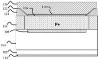
도 2는 본 발명의 추가적인 실시예에 따라 배열된 TVS 다이오드의 일 실시예를 나타내고;
도 3은 본 발명의 추가의 실시예에 따른 TVS 다이오드를 나타내고;
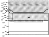
도 4는 본 발명의 추가의 실시예에 따른 다른 TVS 다이오드를 나타내고;
도 5는 본 발명의 더욱 추가의 실시예에 따른 TVS 다이오드를 나타내고;
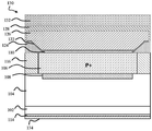
도 6은 본 발명의 추가적인 실시예에 따른 TVS 다이오드를 나타내고;
도 7a 내지 도 7j는 본 발명의 실시예에 따라 TVS 다이오드를 조립하는 공정 흐름을 나타내고;
도 8은 본 발명의 실시예에 따른 예시적인 공정 흐름(800)을 나타낸다.
Claims (19)
- SiC 기판(substrate) 내에 형성된 P-N 다이오드를 포함하고,
상기 SiC 기판 내에 형성된 N-형 영역;
상기 N-형 영역의 상부 부분에 형성된 P-형 영역; 및
상기 P-형 영역과 상기 N-형 영역 사이에 배치된 주입된(implanted) N-형 층
을 포함하는, 디바이스.
- 제1항에 있어서, 상기 N-형 영역은
제1 도핑 수준을 갖는 벌크 기판 영역; 및
상기 벌크 기판 영역과 상기 주입된 N-형 층 사이에 배치되며 상기 제1 도핑 수준보다 작은 제2 도핑 수준을 갖는 에피택셜 SiC 층
을 포함하는, 디바이스.
- 제2항에 있어서, 상기 에피택셜 SiC 층 내에서 상기 P-형 영역 주위에 배치되며 상기 에피택셜 SiC 층의 일부분과 계면 영역을 형성하는 접합 종단 연장 영역(JTE(junction termination extension) 영역)을 추가로 포함하며, 상기 P-형 영역은 제1 p-도핑 수준을 포함하고, 상기 JTE 영역은 상기 제1 p-도핑 수준보다 작은 제2 p-도핑 수준을 갖는 p-형 도펀트를 포함하는, 디바이스.
- 제1항에 있어서, 상기 P-형 영역 주위에 배치되며 상기 N-형 영역과 계면 영역을 형성하는 접합 종단 연장 영역(JTE 영역)을 추가로 포함하며, 상기 P-형 영역은 제1 p-도핑 수준을 포함하고, 상기 JTE 영역은 상기 제1 p-도핑 수준보다 작은 제2 p-도핑 수준을 갖는 p-형 도펀트를 포함하는, 디바이스.
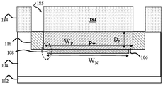
- 제1항에 있어서, 상기 P-형 영역은 하부 표면을 포함하고, 상기 하부 표면은 제1 단부와 제2 단부 사이의 제1 거리만큼 연장되고, 상기 주입된 N-형 층은 상기 하부 표면을 따라 상기 제1 거리보다 작은 제2 거리만큼 연장되며 상기 제1 단부 및 상기 제2 단부로부터 오프셋(offset)되는, 디바이스.
- 제4항에 있어서, 상기 P-형 영역은 하부 표면을 포함하고, 상기 주입된 N-형 층은 상기 하부 표면을 따라 연장되며 상기 접합 종단 연장 영역으로부터 오프셋되는, 디바이스.
- 제1항에 있어서, 20 V 초과 650 V 미만의 항복 전압(breakdown voltage)을 포함하는, 디바이스.
- 제1항에 있어서, 상기 N-형 영역은 벌크 기판 영역을 포함하고, 상기 주입된 N-형 층은 상기 벌크 기판 영역 내에 형성되는, 디바이스.
- 제8항에 있어서, 상기 P-N 다이오드는 20 V 초과 100 V 미만의 항복 전압을 포함하는, 디바이스.
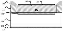
- 제1항에 있어서,
상기 P-형 영역 상에 배치된 애노드 접점; 및
상기 N-형 영역과 접촉하여 상기 SiC 기판의 배면 표면 상에 배치된 배면 접점
을 추가로 포함하는, 디바이스.
- 제10항에 있어서,
상기 P-형 영역 위에서 윈도우(window)를 형성하는 필드 산화물(field oxide) 영역;
상기 애노드 접점과 접촉하여 배치된 금속 층 구조체;
상기 금속 층 구조체 위에 배치된 패시베이션 층; 및
상기 금속 층 구조체 위에 배치된 중합체 층
을 추가로 포함하며, 상기 중합체 층 및 상기 금속 층 구조체는 상기 금속 층 구조체와 접촉하기 위한 개방부를 형성하는, 디바이스.
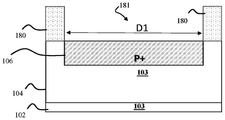
- SiC TVS 다이오드를 형성하는 방법으로서,
SiC 기판에 N-형 영역을 제공하는 단계;
P-형 이온을 주입하여 상기 N-형 영역의 제1 표면으로부터 연장되는 P-형 영역을 형성하는 단계; 및
상기 P-형 영역 밑에 N-형 이온을 주입함으로써 주입된 N-형 층을 형성하는 단계
를 포함하며, 상기 주입된 N-형 층은 상기 P-형 영역과 상기 N-형 영역 사이에 배치되는, 방법.
- 제12항에 있어서, 상기 N-형 영역을 제공하는 단계는,
벌크 기판 영역을 포함하는 SiC 기판을 제공하는 단계로서, 상기 벌크 기판 영역은 제1 도핑 수준의 N-형 도펀트를 갖는, 상기 단계; 및
상기 벌크 기판 영역 상에 에피택셜 SiC 층을 성장시키는 단계로서, 상기 에피택셜 SiC 층은 N-형 도펀트를 포함하며 상기 제1 도핑 수준보다 작은 제2 도핑 수준을 갖는, 상기 단계
를 포함하는, 방법.
- 제13항에 있어서, P-형 도펀트를 주입하여 상기 에피택셜 SiC 층 내에서 상기 P-형 영역 주위에 접합 종단 연장 영역(JTE 영역)을 형성하는 단계를 추가로 포함하며, 상기 P-형 영역은 제1 p-도핑 수준을 포함하고, 상기 JTE 영역의 상기 P-형 도펀트는 상기 제1 p-도핑 수준보다 작은 제2 p-도핑 수준을 포함하는, 방법.
- 제12항에 있어서, 상기 N-형 영역 내에, 상기 P-형 영역 주위에 P-형 도펀트를 주입함으로써 접합 종단 연장 영역(JTE 영역)을 형성하는 단계를 추가로 포함하며, 상기 P-형 영역은 제1 p-도핑 수준을 포함하고, 상기 P-형 도펀트는 상기 제1 p-도핑 수준보다 작은 제2 p-도핑 수준을 갖는, 방법.
- 제12항에 있어서, 상기 주입된 N-형 층을 형성하는 단계는 제1 주입 마스크를 통해 상기 N-형 이온을 주입하는 단계를 포함하고, 상기 P-형 영역을 형성하는 단계는 제2 주입 마스크를 통해 상기 P-형 이온을 주입하는 단계를 포함하며, 상기 제2 주입 마스크는 상기 P-형 영역이 제1 단부와 제2 단부 사이의 제1 거리만큼 연장되도록 배열되고, 상기 제1 주입 마스크는 상기 주입된 N-형 층이 상기 제1 거리보다 작은 제2 거리만큼 연장되고 상기 제1 단부 및 상기 제2 단부로부터 오프셋되도록 배열되는, 방법.
- 제15항에 있어서, 상기 주입된 N-형 층을 형성하는 단계는 제1 주입 마스크를 통해 상기 N-형 이온을 주입하는 단계를 포함하고, 상기 JTE 영역을 형성하는 단계는 JTE 마스크를 통해 상기 P-형 이온을 주입하는 단계를 포함하며, 상기 JTE 마스크는 상기 P-형 영역이 제1 단부와 제2 단부 사이의 제1 거리만큼 연장되도록 배열되고, 상기 제1 주입 마스크는 상기 주입된 N-형 층이 상기 제1 거리보다 작은 제2 거리만큼 연장되고 상기 제1 단부 및 상기 제2 단부로부터 오프셋되도록 배열되는, 방법.
- SiC TVS 디바이스로서,
제1 도펀트 수준을 갖는 N-형 SiC를 포함하는 벌크 기판 영역;
상기 벌크 기판 영역 상에 배치되며, 제2 도펀트 수준을 갖는 N-형 SiC 재료를 포함하는 에피택셜 SiC 층;
상기 에피택셜 SiC 층의 상부 부분에 형성된 P-형 영역; 및
주입된 N-형 층
을 포함하며, 상기 주입된 N-형 층은 상기 에피택셜 SiC 층 내에서 상기 P-형 영역 밑에 배치되고, 상기 주입된 N-형 층은 상기 제2 도펀트 수준보다 큰 제3 도펀트 수준을 포함하는, SiC TVS 디바이스.
- 제18항에 있어서, 20 V 초과 650 V 미만의 항복 전압을 포함하는, SiC TVS 디바이스.
Priority Applications (1)
| Application Number | Priority Date | Filing Date | Title |
|---|---|---|---|
| KR1020240067054A KR102910198B1 (ko) | 2018-09-05 | 2024-05-23 | SiC 기반 보호 디바이스를 위한 구조 및 방법 |
Applications Claiming Priority (2)
| Application Number | Priority Date | Filing Date | Title |
|---|---|---|---|
| US16/121,916 | 2018-09-05 | ||
| US16/121,916 US10910501B2 (en) | 2018-09-05 | 2018-09-05 | Stucture and method for SIC based protection device |
Related Child Applications (1)
| Application Number | Title | Priority Date | Filing Date |
|---|---|---|---|
| KR1020240067054A Division KR102910198B1 (ko) | 2018-09-05 | 2024-05-23 | SiC 기반 보호 디바이스를 위한 구조 및 방법 |
Publications (2)
| Publication Number | Publication Date |
|---|---|
| KR20200027902A true KR20200027902A (ko) | 2020-03-13 |
| KR102670357B1 KR102670357B1 (ko) | 2024-05-30 |
Family
ID=67875262
Family Applications (2)
| Application Number | Title | Priority Date | Filing Date |
|---|---|---|---|
| KR1020190109505A Active KR102670357B1 (ko) | 2018-09-05 | 2019-09-04 | SiC 기반 보호 디바이스를 위한 구조 및 방법 |
| KR1020240067054A Active KR102910198B1 (ko) | 2018-09-05 | 2024-05-23 | SiC 기반 보호 디바이스를 위한 구조 및 방법 |
Family Applications After (1)
| Application Number | Title | Priority Date | Filing Date |
|---|---|---|---|
| KR1020240067054A Active KR102910198B1 (ko) | 2018-09-05 | 2024-05-23 | SiC 기반 보호 디바이스를 위한 구조 및 방법 |
Country Status (5)
| Country | Link |
|---|---|
| US (1) | US10910501B2 (ko) |
| EP (2) | EP4075517A1 (ko) |
| KR (2) | KR102670357B1 (ko) |
| CN (1) | CN110880538B (ko) |
| TW (1) | TWI809185B (ko) |
Families Citing this family (2)
| Publication number | Priority date | Publication date | Assignee | Title |
|---|---|---|---|---|
| CN112928168B (zh) * | 2019-12-06 | 2025-06-27 | 力特半导体(无锡)有限公司 | 具有不对称击穿电压的tvs二极管和组件 |
| TWI862120B (zh) * | 2023-08-30 | 2024-11-11 | 台亞半導體股份有限公司 | 寬能帶二極體及其製造方法 |
Citations (2)
| Publication number | Priority date | Publication date | Assignee | Title |
|---|---|---|---|---|
| US20040070005A1 (en) * | 2002-04-30 | 2004-04-15 | Zarlink Semiconductor Inc. | Compact high voltage ESD protection diode |
| US20130334695A1 (en) * | 2012-06-19 | 2013-12-19 | Nxp B.V. | Electronic device and method of manufacturing such device |
Family Cites Families (14)
| Publication number | Priority date | Publication date | Assignee | Title |
|---|---|---|---|---|
| NL7907680A (nl) | 1979-10-18 | 1981-04-22 | Philips Nv | Zenerdiode. |
| US20070090360A1 (en) * | 2005-10-20 | 2007-04-26 | Vishay General Semiconductors, Llc | Blanket implant diode |
| US8431958B2 (en) * | 2006-11-16 | 2013-04-30 | Alpha And Omega Semiconductor Ltd | Optimized configurations to integrate steering diodes in low capacitance transient voltage suppressor (TVS) |
| CN101383287B (zh) * | 2008-09-27 | 2010-12-08 | 电子科技大学 | 一种垂直双扩散金属氧化物半导体器件的制造方法 |
| US8445917B2 (en) * | 2009-03-20 | 2013-05-21 | Cree, Inc. | Bidirectional silicon carbide transient voltage suppression devices |
| US9048106B2 (en) * | 2012-12-13 | 2015-06-02 | Diodes Incorporated | Semiconductor diode assembly |
| US9425153B2 (en) * | 2013-04-04 | 2016-08-23 | Monolith Semiconductor Inc. | Semiconductor devices comprising getter layers and methods of making and using the same |
| US9431385B2 (en) * | 2013-08-09 | 2016-08-30 | Semiconductor Components Industries, Llc | Semiconductor component that includes a common mode filter and method of manufacturing the semiconductor component |
| US9478606B2 (en) | 2014-02-13 | 2016-10-25 | Microsemi Corporation | SiC transient voltage suppressor |
| DE102015118165A1 (de) * | 2015-10-23 | 2017-04-27 | Infineon Technologies Ag | Elektrische baugruppe, umfassend eine halbleiterschaltvorrichtung und eine klemmdiode |
| JP6705155B2 (ja) * | 2015-11-13 | 2020-06-03 | 富士電機株式会社 | 半導体装置および半導体装置の製造方法 |
| US20190140444A1 (en) * | 2016-04-15 | 2019-05-09 | Littelfuse Semiconductor (Wuxi) Co., Ltd. | Overvoltage Protection and Linear Regulator Device Module |
| JP6855793B2 (ja) * | 2016-12-28 | 2021-04-07 | 富士電機株式会社 | 半導体装置 |
| CN106847879B (zh) * | 2017-01-19 | 2021-12-03 | 北京世纪金光半导体有限公司 | 一种斜面沟道的SiC MOSFET器件及制备方法 |
-
2018
- 2018-09-05 US US16/121,916 patent/US10910501B2/en active Active
-
2019
- 2019-09-02 TW TW108131452A patent/TWI809185B/zh active
- 2019-09-03 CN CN201910831358.1A patent/CN110880538B/zh active Active
- 2019-09-04 KR KR1020190109505A patent/KR102670357B1/ko active Active
- 2019-09-05 EP EP22176219.8A patent/EP4075517A1/en active Pending
- 2019-09-05 EP EP19195719.0A patent/EP3621121A1/en not_active Ceased
-
2024
- 2024-05-23 KR KR1020240067054A patent/KR102910198B1/ko active Active
Patent Citations (2)
| Publication number | Priority date | Publication date | Assignee | Title |
|---|---|---|---|---|
| US20040070005A1 (en) * | 2002-04-30 | 2004-04-15 | Zarlink Semiconductor Inc. | Compact high voltage ESD protection diode |
| US20130334695A1 (en) * | 2012-06-19 | 2013-12-19 | Nxp B.V. | Electronic device and method of manufacturing such device |
Also Published As
| Publication number | Publication date |
|---|---|
| US20200075780A1 (en) | 2020-03-05 |
| TWI809185B (zh) | 2023-07-21 |
| US10910501B2 (en) | 2021-02-02 |
| EP3621121A1 (en) | 2020-03-11 |
| KR102670357B1 (ko) | 2024-05-30 |
| KR102910198B1 (ko) | 2026-01-09 |
| EP4075517A1 (en) | 2022-10-19 |
| KR20240078639A (ko) | 2024-06-04 |
| TW202013672A (zh) | 2020-04-01 |
| CN110880538B (zh) | 2025-11-28 |
| CN110880538A (zh) | 2020-03-13 |
Similar Documents
| Publication | Publication Date | Title |
|---|---|---|
| EP2183833B1 (en) | Epitaxial surge protection device | |
| US9679998B2 (en) | Bi-directional punch-through semiconductor device and manufacturing method thereof | |
| KR102910198B1 (ko) | SiC 기반 보호 디바이스를 위한 구조 및 방법 | |
| EP2183832B1 (en) | Low capacitance semiconductor device | |
| CN113646901B (zh) | 具有浪涌电流稳定性的肖特基整流器及其制造方法 | |
| Lynch et al. | Design considerations for high voltage SiC power devices: An experimental investigation into channel pinching of 10kV SiC junction barrier schottky (JBS) diodes | |
| US9831327B2 (en) | Electrostatic discharge protection devices and methods of forming the same | |
| KR101800331B1 (ko) | 개선된 역서지 내량 및 감소된 누설 전류를 위한 폴리실리콘 층을 갖는 제너 다이오드 | |
| US7238553B1 (en) | Method of forming a high-voltage silicon controlled rectifier structure with improved punch through resistance | |
| CN107293533A (zh) | 瞬态电压抑制器及其制造方法 | |
| CN107301996B (zh) | 瞬态电压抑制器及其制造方法 | |
| EP4340045A1 (en) | Bidirectional asymmetric transient voltage suppressor device | |
| CN219303673U (zh) | 单向高电压穿通瞬态电压抑制器件 | |
| CN219040487U (zh) | 非对称双向瞬态电压抑制器件 | |
| KR102852308B1 (ko) | 과도 전압 억제 소자 및 그 제조 방법 | |
| CN113284938B (zh) | 半导体装置及半导体装置的制造方法 | |
| CN107301997B (zh) | 瞬态电压抑制器及其制造方法 | |
| CN117917780A (zh) | 单向高电压穿通tvs二极管及制造方法 |
Legal Events
| Date | Code | Title | Description |
|---|---|---|---|
| PA0109 | Patent application |
St.27 status event code: A-0-1-A10-A12-nap-PA0109 |
|
| R18-X000 | Changes to party contact information recorded |
St.27 status event code: A-3-3-R10-R18-oth-X000 |
|
| P11-X000 | Amendment of application requested |
St.27 status event code: A-2-2-P10-P11-nap-X000 |
|
| P13-X000 | Application amended |
St.27 status event code: A-2-2-P10-P13-nap-X000 |
|
| PG1501 | Laying open of application |
St.27 status event code: A-1-1-Q10-Q12-nap-PG1501 |
|
| A201 | Request for examination | ||
| PA0201 | Request for examination |
St.27 status event code: A-1-2-D10-D11-exm-PA0201 |
|
| D13-X000 | Search requested |
St.27 status event code: A-1-2-D10-D13-srh-X000 |
|
| D14-X000 | Search report completed |
St.27 status event code: A-1-2-D10-D14-srh-X000 |
|
| E902 | Notification of reason for refusal | ||
| PE0902 | Notice of grounds for rejection |
St.27 status event code: A-1-2-D10-D21-exm-PE0902 |
|
| AMND | Amendment | ||
| E13-X000 | Pre-grant limitation requested |
St.27 status event code: A-2-3-E10-E13-lim-X000 |
|
| P11-X000 | Amendment of application requested |
St.27 status event code: A-2-2-P10-P11-nap-X000 |
|
| P13-X000 | Application amended |
St.27 status event code: A-2-2-P10-P13-nap-X000 |
|
| E601 | Decision to refuse application | ||
| PE0601 | Decision on rejection of patent |
St.27 status event code: N-2-6-B10-B15-exm-PE0601 |
|
| AMND | Amendment | ||
| E13-X000 | Pre-grant limitation requested |
St.27 status event code: A-2-3-E10-E13-lim-X000 |
|
| P11-X000 | Amendment of application requested |
St.27 status event code: A-2-2-P10-P11-nap-X000 |
|
| P13-X000 | Application amended |
St.27 status event code: A-2-2-P10-P13-nap-X000 |
|
| PX0901 | Re-examination |
St.27 status event code: A-2-3-E10-E12-rex-PX0901 |
|
| PX0701 | Decision of registration after re-examination |
St.27 status event code: A-3-4-F10-F13-rex-PX0701 |
|
| X701 | Decision to grant (after re-examination) | ||
| PA0107 | Divisional application |
St.27 status event code: A-0-1-A10-A18-div-PA0107 St.27 status event code: A-0-1-A10-A16-div-PA0107 |
|
| PR0701 | Registration of establishment |
St.27 status event code: A-2-4-F10-F11-exm-PR0701 |
|
| PR1002 | Payment of registration fee |
St.27 status event code: A-2-2-U10-U11-oth-PR1002 Fee payment year number: 1 |
|
| PG1601 | Publication of registration |
St.27 status event code: A-4-4-Q10-Q13-nap-PG1601 |
|
| P22-X000 | Classification modified |
St.27 status event code: A-4-4-P10-P22-nap-X000 |
|
| P22-X000 | Classification modified |
St.27 status event code: A-4-4-P10-P22-nap-X000 |