KR20200028016A - 검사 장치, 검사 방법 및 기억 매체 - Google Patents
검사 장치, 검사 방법 및 기억 매체 Download PDFInfo
- Publication number
- KR20200028016A KR20200028016A KR1020207005151A KR20207005151A KR20200028016A KR 20200028016 A KR20200028016 A KR 20200028016A KR 1020207005151 A KR1020207005151 A KR 1020207005151A KR 20207005151 A KR20207005151 A KR 20207005151A KR 20200028016 A KR20200028016 A KR 20200028016A
- Authority
- KR
- South Korea
- Prior art keywords
- electrode
- needle
- imaging
- inspection
- imaging unit
- Prior art date
- Legal status (The legal status is an assumption and is not a legal conclusion. Google has not performed a legal analysis and makes no representation as to the accuracy of the status listed.)
- Granted
Links
Images




Classifications
-
- G—PHYSICS
- G01—MEASURING; TESTING
- G01R—MEASURING ELECTRIC VARIABLES; MEASURING MAGNETIC VARIABLES
- G01R31/00—Arrangements for testing electric properties; Arrangements for locating electric faults; Arrangements for electrical testing characterised by what is being tested not provided for elsewhere
- G01R31/28—Testing of electronic circuits, e.g. by signal tracer
- G01R31/2851—Testing of integrated circuits [IC]
- G01R31/2886—Features relating to contacting the IC under test, e.g. probe heads; chucks
- G01R31/2891—Features relating to contacting the IC under test, e.g. probe heads; chucks related to sensing or controlling of force, position, temperature
-
- G—PHYSICS
- G01—MEASURING; TESTING
- G01N—INVESTIGATING OR ANALYSING MATERIALS BY DETERMINING THEIR CHEMICAL OR PHYSICAL PROPERTIES
- G01N21/00—Investigating or analysing materials by the use of optical means, i.e. using sub-millimetre waves, infrared, visible or ultraviolet light
- G01N21/84—Systems specially adapted for particular applications
- G01N21/88—Investigating the presence of flaws or contamination
- G01N21/8851—Scan or image signal processing specially adapted therefor, e.g. for scan signal adjustment, for detecting different kinds of defects, for compensating for structures, markings, edges
-
- G—PHYSICS
- G01—MEASURING; TESTING
- G01N—INVESTIGATING OR ANALYSING MATERIALS BY DETERMINING THEIR CHEMICAL OR PHYSICAL PROPERTIES
- G01N21/00—Investigating or analysing materials by the use of optical means, i.e. using sub-millimetre waves, infrared, visible or ultraviolet light
- G01N21/84—Systems specially adapted for particular applications
- G01N21/88—Investigating the presence of flaws or contamination
- G01N21/8806—Specially adapted optical and illumination features
-
- G—PHYSICS
- G01—MEASURING; TESTING
- G01R—MEASURING ELECTRIC VARIABLES; MEASURING MAGNETIC VARIABLES
- G01R1/00—Details of instruments or arrangements of the types included in groups G01R5/00 - G01R13/00 and G01R31/00
- G01R1/02—General constructional details
- G01R1/04—Housings; Supporting members; Arrangements of terminals
- G01R1/0408—Test fixtures or contact fields; Connectors or connecting adaptors; Test clips; Test sockets
-
- G—PHYSICS
- G01—MEASURING; TESTING
- G01R—MEASURING ELECTRIC VARIABLES; MEASURING MAGNETIC VARIABLES
- G01R31/00—Arrangements for testing electric properties; Arrangements for locating electric faults; Arrangements for electrical testing characterised by what is being tested not provided for elsewhere
- G01R31/28—Testing of electronic circuits, e.g. by signal tracer
- G01R31/2851—Testing of integrated circuits [IC]
- G01R31/2886—Features relating to contacting the IC under test, e.g. probe heads; chucks
-
- G—PHYSICS
- G01—MEASURING; TESTING
- G01R—MEASURING ELECTRIC VARIABLES; MEASURING MAGNETIC VARIABLES
- G01R31/00—Arrangements for testing electric properties; Arrangements for locating electric faults; Arrangements for electrical testing characterised by what is being tested not provided for elsewhere
- G01R31/28—Testing of electronic circuits, e.g. by signal tracer
- G01R31/2851—Testing of integrated circuits [IC]
- G01R31/2886—Features relating to contacting the IC under test, e.g. probe heads; chucks
- G01R31/2887—Features relating to contacting the IC under test, e.g. probe heads; chucks involving moving the probe head or the IC under test; docking stations
-
- G—PHYSICS
- G01—MEASURING; TESTING
- G01R—MEASURING ELECTRIC VARIABLES; MEASURING MAGNETIC VARIABLES
- G01R31/00—Arrangements for testing electric properties; Arrangements for locating electric faults; Arrangements for electrical testing characterised by what is being tested not provided for elsewhere
- G01R31/28—Testing of electronic circuits, e.g. by signal tracer
- G01R31/2851—Testing of integrated circuits [IC]
- G01R31/2886—Features relating to contacting the IC under test, e.g. probe heads; chucks
- G01R31/2889—Interfaces, e.g. between probe and tester
-
- G—PHYSICS
- G01—MEASURING; TESTING
- G01R—MEASURING ELECTRIC VARIABLES; MEASURING MAGNETIC VARIABLES
- G01R31/00—Arrangements for testing electric properties; Arrangements for locating electric faults; Arrangements for electrical testing characterised by what is being tested not provided for elsewhere
- G01R31/28—Testing of electronic circuits, e.g. by signal tracer
- G01R31/2851—Testing of integrated circuits [IC]
- G01R31/2893—Handling, conveying or loading, e.g. belts, boats, vacuum fingers
-
- G—PHYSICS
- G06—COMPUTING OR CALCULATING; COUNTING
- G06T—IMAGE DATA PROCESSING OR GENERATION, IN GENERAL
- G06T7/00—Image analysis
- G06T7/0002—Inspection of images, e.g. flaw detection
- G06T7/0004—Industrial image inspection
-
- G—PHYSICS
- G01—MEASURING; TESTING
- G01N—INVESTIGATING OR ANALYSING MATERIALS BY DETERMINING THEIR CHEMICAL OR PHYSICAL PROPERTIES
- G01N21/00—Investigating or analysing materials by the use of optical means, i.e. using sub-millimetre waves, infrared, visible or ultraviolet light
- G01N21/84—Systems specially adapted for particular applications
- G01N21/88—Investigating the presence of flaws or contamination
- G01N21/8851—Scan or image signal processing specially adapted therefor, e.g. for scan signal adjustment, for detecting different kinds of defects, for compensating for structures, markings, edges
- G01N2021/8854—Grading and classifying of flaws
- G01N2021/8867—Grading and classifying of flaws using sequentially two or more inspection runs, e.g. coarse and fine, or detecting then analysing
-
- G—PHYSICS
- G01—MEASURING; TESTING
- G01N—INVESTIGATING OR ANALYSING MATERIALS BY DETERMINING THEIR CHEMICAL OR PHYSICAL PROPERTIES
- G01N21/00—Investigating or analysing materials by the use of optical means, i.e. using sub-millimetre waves, infrared, visible or ultraviolet light
- G01N21/84—Systems specially adapted for particular applications
- G01N21/88—Investigating the presence of flaws or contamination
- G01N21/8851—Scan or image signal processing specially adapted therefor, e.g. for scan signal adjustment, for detecting different kinds of defects, for compensating for structures, markings, edges
- G01N2021/8887—Scan or image signal processing specially adapted therefor, e.g. for scan signal adjustment, for detecting different kinds of defects, for compensating for structures, markings, edges based on image processing techniques
Landscapes
- Engineering & Computer Science (AREA)
- Physics & Mathematics (AREA)
- General Physics & Mathematics (AREA)
- Computer Hardware Design (AREA)
- Microelectronics & Electronic Packaging (AREA)
- General Engineering & Computer Science (AREA)
- Biochemistry (AREA)
- Computer Vision & Pattern Recognition (AREA)
- Health & Medical Sciences (AREA)
- General Health & Medical Sciences (AREA)
- Analytical Chemistry (AREA)
- Immunology (AREA)
- Pathology (AREA)
- Life Sciences & Earth Sciences (AREA)
- Chemical & Material Sciences (AREA)
- Signal Processing (AREA)
- Theoretical Computer Science (AREA)
- Quality & Reliability (AREA)
- Testing Or Measuring Of Semiconductors Or The Like (AREA)
- Investigating Materials By The Use Of Optical Means Adapted For Particular Applications (AREA)
- Analysing Materials By The Use Of Radiation (AREA)
Abstract
Description
도 2는, 프로버가 구비하는 본체의 내부 구조의 개략을 도시하는 사시도이다.
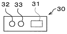
도 3은, 하부 촬상 유닛의 모식 상면도이다.
도 4는, 상부 촬상 유닛의 모식 하면도이다.
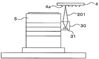
도 5는, 본 발명의 실시 형태에 관한 검사 처리의 일 공정의 설명도이다.
도 6은, 본 발명의 실시 형태에 관한 검사 처리의 다른 공정의 설명도이다.
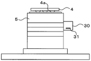
도 7은, 본 발명의 실시 형태에 관한 검사 처리의 다른 공정의 설명도이다.
도 8은, 본 발명의 실시 형태에 관한 검사 처리의 또 다른 공정의 설명도이다.
2: 로더부
3: 테스트 헤드
4: 프로브 카드
4a: 프로브 바늘
5: 스테이지
7: 제어부
10: 기대
11: X 방향 이동 유닛
12: Y 방향 이동 유닛
13: Z 방향 이동 유닛
30: 하부 촬상 유닛
31: 하부 카메라
32: 저배율 렌즈
33: 고배율 렌즈
50: 상부 촬상 유닛
51: 상부 카메라
52: 저배율 렌즈
53: 고배율 렌즈
60: 타깃판
100: 프로버
Claims (16)
- 피검사체에 형성된 전극에 프로브 바늘이 접촉함으로써 상기 전극에 발생하는 바늘자국을 검사하는 검사 장치이며,
비닝 기능을 갖는 촬상부와,
적어도 상기 촬상부를 제어하는 제어부를 구비하고,
상기 제어부는,
상기 프로브 바늘의 접촉 동작 후의 상기 전극을, 상기 비닝 기능을 유효로 한 상기 촬상부로 하여금 촬상시키고, 이때의 촬상 결과에 기초하여, 상기 전극에 대하여 상기 바늘자국의 상태의 판정을 행하는 고속 저정밀도 검사 공정과,
상기 고속 저정밀도 검사 공정에서의 판정 결과에 따라, 상기 비닝 기능을 무효로 한 상기 촬상부로 하여금 다시 촬상시키고, 이때의 촬상 결과에 기초하여, 다시 촬상된 상기 전극의 상기 바늘자국의 상태의 판정을 행하는 저속 고정밀도 검사 공정
을 실행하도록 구성되어 있는, 검사 장치. - 제1항에 있어서,
상기 저속 고정밀도 검사 공정에서는, 상기 고속 저정밀도 검사 공정에서 상기 바늘자국의 상태의 판정 대상으로 된 상기 전극 중, 당해 고속 저정밀도 검사 공정에서의 판정 결과에 따라 선택된 전극만을 상기 바늘자국의 상태의 판정 대상으로 하는, 검사 장치. - 제2항에 있어서,
상기 선택된 전극은, 상기 고속 저정밀도 검사 공정에 있어서 재검사 필요라고 판정된 전극인, 검사 장치. - 제1항에 있어서,
상기 고속 저정밀도 검사 공정에서는, 상기 전극에 대하여, 상기 바늘자국이 양호한지, 재검사가 필요한지, 또는 상기 바늘자국이 불량한지를 판정하고,
상기 저속 고정밀도 검사 공정에서는, 상기 전극에 대하여, 상기 바늘자국이 양호한지, 또는 상기 바늘자국이 불량한지를 판정하는, 검사 장치. - 제4항에 있어서,
상기 고속 저정밀도 검사 공정에서는, 상기 전극에 있어서의 소정의 영역 내에, 면적이 소정의 범위 내에 어떤 소정의 수의 상기 바늘자국이 인식된 경우, 당해 전극에 대하여 바늘자국이 양호라고 판정하는, 검사 장치. - 제4항에 있어서,
상기 고속 저정밀도 검사 공정에 있어서,
상기 바늘자국이 인식되지 않는 경우,
상기 전극에 있어서의 소정의 영역 내에서 인식된 상기 바늘자국의 수가 소정의 수와 일치하지 않는 경우,
상기 전극에 있어서의 경계 부분에서 상기 바늘자국이 인식된 경우,
또는, 상기 전극에 있어서의 소정의 영역 내에서 인식된 상기 바늘자국이 엷은 경우에는,
당해 전극에 대하여 재검사 필요라고 판정하는, 검사 장치. - 제4항에 있어서,
상기 고속 저정밀도 검사 공정에 있어서,
상기 전극 이외의 부분에 상기 바늘자국이 인식된 경우,
또는, 상기 전극에 있어서의 소정의 영역 내에서 인식된 상기 바늘자국의 면적이 소정의 범위 내에 없는 경우에는,
당해 전극에 대하여 상기 바늘자국이 불량이라고 판정하는, 검사 장치. - 제4항에 있어서,
상기 저속 고정밀도 검사 공정에 있어서, 상기 전극에 있어서의 소정의 영역 내에, 면적이 소정의 범위 내에 어떤 소정의 수의 상기 바늘자국이 있는 경우에는, 당해 전극에 대하여 상기 바늘자국이 양호라고 판정하는, 검사 장치. - 제4항에 있어서,
상기 저속 고정밀도 검사 공정에 있어서,
상기 전극에 있어서의 소정의 영역 이외의 부분에 상기 바늘자국이 인식된 경우,
상기 전극에 있어서의 소정의 영역 내에서 인식된 상기 바늘자국의 면적이 소정의 범위 내에 없는 경우,
상기 바늘자국이 인식되지 않는 경우,
또는, 상기 전극에 있어서의 소정의 영역 내에서 인식된 상기 바늘자국의 수가 소정의 수와 일치하지 않는 경우에는,
당해 전극에 대하여 상기 바늘자국이 불량이라고 판정하는, 검사 장치. - 제1항에 있어서,
상기 비닝 기능을 유효로 한 경우의 가상적인 해상도보다 낮은 해상도로 상기 촬상부에 의한 촬상을 행하기 위한 저해상도 광학계를 구비하고,
상기 제어부는,
상기 저해상도 광학계를 통한 상기 촬상부에 의한 상기 피검사체의 촬상 결과와, 상기 저해상도 광학계를 통하지 않는 상기 촬상부에 의한 상기 피검사체의 촬상 결과에 기초하여, 상기 피검사체의 기준 위치의 정보를 취득하는 기준 위치 정보 취득 공정
을 실행하도록 구성되어 있는, 검사 장치. - 제1항에 있어서,
상기 제어부는,
상기 비닝 기능을 유효로 한 상기 촬상부로 하여금, 상기 피검사체가 적재되는 적재대를 촬상시키고, 촬상 결과에 기초하여, 상기 적재대 상의 이물의 유무를 판정하도록 구성되어 있는, 검사 장치. - 제1항에 있어서,
상기 검사 장치는, 상기 피검사체에 형성된 상기 전극에 상기 프로브 바늘을 접촉시키고, 상기 프로브 바늘을 통하여 상기 피검사체에 전기 신호를 공급함으로써 상기 피검사체를 검사하는 프로브 장치이며,
상기 프로브 바늘을 촬상하는 별도의 촬상부를 구비하고,
상기 제어부는,
상기 촬상부와 상기 별도의 촬상부의 위치 정렬을 위한 타깃 마크를, 상기 비닝 기능을 유효로 한 상기 촬상부로 하여금 촬상시키고, 촬상 결과에 기초하여 상기 위치 정렬을 행하는 촬상부 위치 정렬 공정을
실행하도록 구성되어 있는, 검사 장치. - 제1항에 있어서,
상기 검사 장치는, 상기 피검사체에 형성된 상기 전극에 상기 프로브 바늘을 접촉시키고, 상기 프로브 바늘을 통하여 상기 피검사체에 전기 신호를 공급함으로써 상기 피검사체를 검사하는 프로브 장치이며,
상기 프로브 바늘을 촬상하는 별도의 촬상부를 구비하고,
상기 제어부는, 상기 비닝 기능을 유효로 하여 촬상한 상기 촬상부로부터의 출력에 기초하여, 당해 촬상부와 상기 별도의 촬상부의 위치 정렬을 행하는 촬상부 위치 정렬 공정을
실행하도록 구성되어 있는, 검사 장치. - 피검사체에 형성된 전극에 프로브 바늘이 접촉함으로써 상기 전극에 발생하는 바늘자국을 검사하는 검사 장치를 사용한 검사 방법이며,
상기 검사 장치는, 비닝 기능을 갖는 촬상부를 구비하고,
상기 프로브 바늘의 접촉 동작 후의 상기 전극을, 상기 비닝 기능을 유효로 한 상기 촬상부로 하여금 촬상시키고, 촬상 결과에 기초하여, 상기 전극에 대한 상기 바늘자국의 상태의 판정을 행하는 고속 저정밀도 검사 공정과,
해당 고속 저정밀도 검사 공정에서의 판정 결과에 따라, 상기 비닝 기능을 무효로 한 상기 촬상부로 하여금 다시 촬상시키고, 촬상 결과에 기초하여, 다시 촬상된 전극의 상기 바늘자국의 상태의 판정을 행하는 저속 고정밀도 검사 공정을 포함하는, 검사 방법. - 검사 장치에 의해 검사 방법을 실행시키도록, 당해 검사 장치를 제어하는 제어부의 컴퓨터 상에서 동작하는 프로그램을 저장한 판독 가능한 컴퓨터 기억 매체이며,
상기 검사 장치는, 비닝 기능을 갖는 촬상부를 구비하고,
상기 검사 방법은, 피검사체에 형성된 전극에 프로브 바늘이 접촉함으로써 상기 전극에 발생하는 바늘자국을 검사하는 검사 장치를 사용한 검사 방법이며,
상기 프로브 바늘의 접촉 동작 후의 상기 전극을, 상기 비닝 기능을 유효로 한 상기 촬상부로 하여금 촬상시키고, 촬상 결과에 기초하여, 상기 전극에 대한 상기 바늘자국의 상태의 판정을 행하는 고속 저정밀도 검사 공정과,
해당 고속 저정밀도 검사 공정에서의 판정 결과에 따라, 상기 비닝 기능을 무효로 한 상기 촬상부로 하여금 다시 촬상시키고, 촬상 결과에 기초하여, 다시 촬상된 전극의 상기 바늘자국의 상태의 판정을 행하는 저속 고정밀도 검사 공정을 포함하는, 기억 매체. - 피검사체에 형성된 전극에 프로브 바늘을 접촉시키고, 상기 프로브 바늘을 통하여 상기 피검사체에 전기 신호를 공급함으로써 상기 피검사체를 검사하는 검사 장치이며,
비닝 기능을 갖는 촬상부와,
상기 비닝 기능을 유효로 한 경우의 가상적인 해상도보다 낮은 해상도로 상기 촬상부에 의한 촬상을 행하기 위한 광학계를 구비하는, 검사 장치.
Applications Claiming Priority (3)
| Application Number | Priority Date | Filing Date | Title |
|---|---|---|---|
| JPJP-P-2017-148199 | 2017-07-31 | ||
| JP2017148199A JP6999321B2 (ja) | 2017-07-31 | 2017-07-31 | 検査装置、検査方法及び記憶媒体 |
| PCT/JP2018/026724 WO2019026607A1 (ja) | 2017-07-31 | 2018-07-17 | 検査装置、検査方法及び記憶媒体 |
Publications (2)
| Publication Number | Publication Date |
|---|---|
| KR20200028016A true KR20200028016A (ko) | 2020-03-13 |
| KR102219110B1 KR102219110B1 (ko) | 2021-02-22 |
Family
ID=65232751
Family Applications (1)
| Application Number | Title | Priority Date | Filing Date |
|---|---|---|---|
| KR1020207005151A Active KR102219110B1 (ko) | 2017-07-31 | 2018-07-17 | 검사 장치, 검사 방법 및 기억 매체 |
Country Status (6)
| Country | Link |
|---|---|
| US (1) | US11221363B2 (ko) |
| JP (1) | JP6999321B2 (ko) |
| KR (1) | KR102219110B1 (ko) |
| CN (1) | CN110998815B (ko) |
| TW (1) | TWI772465B (ko) |
| WO (1) | WO2019026607A1 (ko) |
Cited By (1)
| Publication number | Priority date | Publication date | Assignee | Title |
|---|---|---|---|---|
| KR102718594B1 (ko) * | 2023-08-29 | 2024-10-16 | 백상삼 | 기판의 찍힘 불량 검사 장치 및 방법 |
Families Citing this family (4)
| Publication number | Priority date | Publication date | Assignee | Title |
|---|---|---|---|---|
| CN112858337B (zh) * | 2021-03-25 | 2024-12-03 | 深圳中科飞测科技股份有限公司 | 检测方法、检测设备、检测装置及存储介质 |
| US12148144B2 (en) * | 2022-04-19 | 2024-11-19 | Nanya Technology Corporation | Wafer inspection system |
| US12211200B2 (en) * | 2022-04-19 | 2025-01-28 | Nanya Technology Corporation | Wafer inspection system method |
| TWI881784B (zh) * | 2024-04-03 | 2025-04-21 | 黑澤科技股份有限公司 | 治具對位補償方法 |
Citations (6)
| Publication number | Priority date | Publication date | Assignee | Title |
|---|---|---|---|---|
| JPH07147304A (ja) | 1993-11-24 | 1995-06-06 | Tokyo Electron Ltd | オートセットアップ式プローブ検査方法 |
| JPH11230917A (ja) * | 1998-02-12 | 1999-08-27 | Nikon Corp | 欠陥検査装置 |
| JP2008139795A (ja) * | 2006-12-05 | 2008-06-19 | Keyence Corp | 拡大画像観察装置、拡大画像観察方法、拡大画像観察プログラム及びコンピュータで読み取り可能な記録媒体並びに記録した機器 |
| JP2009099937A (ja) * | 2007-09-28 | 2009-05-07 | Tokyo Electron Ltd | プローブ装置及びプロービング方法 |
| JP2012242297A (ja) * | 2011-05-20 | 2012-12-10 | Canon Inc | 撮像システム、画像処理装置 |
| JP5326359B2 (ja) * | 2008-05-23 | 2013-10-30 | 東京エレクトロン株式会社 | 針跡検査装置、プローブ装置、及び針跡検査方法、並びに記憶媒体 |
Family Cites Families (18)
| Publication number | Priority date | Publication date | Assignee | Title |
|---|---|---|---|---|
| JP2896153B2 (ja) * | 1989-03-09 | 1999-05-31 | 株式会社東芝 | 自動検査装置 |
| JPH02280035A (ja) * | 1989-04-21 | 1990-11-16 | Seiko Epson Corp | 画像処理による電極パターンの検査方法 |
| JP3173676B2 (ja) * | 1992-03-23 | 2001-06-04 | 東京エレクトロン株式会社 | プローブ装置 |
| JPH09203765A (ja) * | 1996-01-25 | 1997-08-05 | Hioki Ee Corp | ビジュアル併用型基板検査装置 |
| US5999268A (en) * | 1996-10-18 | 1999-12-07 | Tokyo Electron Limited | Apparatus for aligning a semiconductor wafer with an inspection contactor |
| JP3303968B2 (ja) * | 1998-02-19 | 2002-07-22 | 東京エレクトロン株式会社 | ウエハと接触子の位置合わせ装置 |
| JP2004152916A (ja) * | 2002-10-29 | 2004-05-27 | Nec Corp | 半導体デバイス検査装置及び検査方法 |
| JP2005150224A (ja) * | 2003-11-12 | 2005-06-09 | Nec Electronics Corp | プローブ情報を用いた半導体検査装置及び検査方法 |
| JP4908138B2 (ja) * | 2005-12-09 | 2012-04-04 | ルネサスエレクトロニクス株式会社 | プローブ検査装置 |
| JP4804295B2 (ja) * | 2006-09-21 | 2011-11-02 | ヤマハ発動機株式会社 | 部品認識方法、部品認識装置、表面実装機及び部品検査装置 |
| JP2009296451A (ja) * | 2008-06-06 | 2009-12-17 | Hamamatsu Photonics Kk | 固体撮像装置 |
| WO2010073359A1 (ja) * | 2008-12-26 | 2010-07-01 | 富士通セミコンダクター株式会社 | プローバ、試験装置、及び半導体チップの検査方法 |
| JP5433266B2 (ja) * | 2009-03-19 | 2014-03-05 | 東京エレクトロン株式会社 | 針跡の判定方法及び針跡判定用プログラム |
| JP5544344B2 (ja) * | 2011-09-26 | 2014-07-09 | 株式会社日立ハイテクノロジーズ | 欠陥観察方法及び欠陥観察装置 |
| JP5821708B2 (ja) * | 2012-03-06 | 2015-11-24 | トヨタ自動車株式会社 | 欠陥検査装置及び欠陥検査方法 |
| JP6462296B2 (ja) * | 2014-09-30 | 2019-01-30 | 東京エレクトロン株式会社 | 位置精度検査方法、位置精度検査装置及び位置検査ユニット |
| JP6415281B2 (ja) | 2014-12-05 | 2018-10-31 | 東京エレクトロン株式会社 | プローブ装置及びプローブ方法 |
| TWI606532B (zh) * | 2017-04-17 | 2017-11-21 | 旺矽科技股份有限公司 | 微發光二極體晶圓的測試方法 |
-
2017
- 2017-07-31 JP JP2017148199A patent/JP6999321B2/ja active Active
-
2018
- 2018-07-17 TW TW107124587A patent/TWI772465B/zh active
- 2018-07-17 WO PCT/JP2018/026724 patent/WO2019026607A1/ja not_active Ceased
- 2018-07-17 US US16/633,789 patent/US11221363B2/en active Active
- 2018-07-17 CN CN201880050591.XA patent/CN110998815B/zh active Active
- 2018-07-17 KR KR1020207005151A patent/KR102219110B1/ko active Active
Patent Citations (6)
| Publication number | Priority date | Publication date | Assignee | Title |
|---|---|---|---|---|
| JPH07147304A (ja) | 1993-11-24 | 1995-06-06 | Tokyo Electron Ltd | オートセットアップ式プローブ検査方法 |
| JPH11230917A (ja) * | 1998-02-12 | 1999-08-27 | Nikon Corp | 欠陥検査装置 |
| JP2008139795A (ja) * | 2006-12-05 | 2008-06-19 | Keyence Corp | 拡大画像観察装置、拡大画像観察方法、拡大画像観察プログラム及びコンピュータで読み取り可能な記録媒体並びに記録した機器 |
| JP2009099937A (ja) * | 2007-09-28 | 2009-05-07 | Tokyo Electron Ltd | プローブ装置及びプロービング方法 |
| JP5326359B2 (ja) * | 2008-05-23 | 2013-10-30 | 東京エレクトロン株式会社 | 針跡検査装置、プローブ装置、及び針跡検査方法、並びに記憶媒体 |
| JP2012242297A (ja) * | 2011-05-20 | 2012-12-10 | Canon Inc | 撮像システム、画像処理装置 |
Cited By (1)
| Publication number | Priority date | Publication date | Assignee | Title |
|---|---|---|---|---|
| KR102718594B1 (ko) * | 2023-08-29 | 2024-10-16 | 백상삼 | 기판의 찍힘 불량 검사 장치 및 방법 |
Also Published As
| Publication number | Publication date |
|---|---|
| KR102219110B1 (ko) | 2021-02-22 |
| JP6999321B2 (ja) | 2022-01-18 |
| CN110998815A (zh) | 2020-04-10 |
| TW201913847A (zh) | 2019-04-01 |
| WO2019026607A1 (ja) | 2019-02-07 |
| US11221363B2 (en) | 2022-01-11 |
| TWI772465B (zh) | 2022-08-01 |
| US20200241069A1 (en) | 2020-07-30 |
| CN110998815B (zh) | 2023-10-27 |
| JP2019029531A (ja) | 2019-02-21 |
Similar Documents
| Publication | Publication Date | Title |
|---|---|---|
| KR102219110B1 (ko) | 검사 장치, 검사 방법 및 기억 매체 | |
| KR101865887B1 (ko) | 위치 정밀도 검사 방법, 위치 정밀도 검사 장치 및 위치 검사 유닛 | |
| KR100786463B1 (ko) | 두 물체의 위치 정렬 방법, 두 물체의 중첩 상태의 검출방법 및 두 물체의 위치 정렬 장치 | |
| KR100284558B1 (ko) | 프로우빙 방법 및 프로우브 장치 | |
| US7724007B2 (en) | Probe apparatus and probing method | |
| KR101071013B1 (ko) | 검사 방법 및 이 검사 방법을 기록한 프로그램 기록 매체 | |
| US10310010B2 (en) | Probe apparatus and probe method | |
| US5416592A (en) | Probe apparatus for measuring electrical characteristics of objects | |
| JP2009099937A (ja) | プローブ装置及びプロービング方法 | |
| US20190187180A1 (en) | Prober | |
| JP3173676B2 (ja) | プローブ装置 | |
| JP3248136B1 (ja) | プローブ方法及びプローブ装置 | |
| JPH05198662A (ja) | プローブ装置及び同装置におけるアライメント方法 | |
| JP2002057196A (ja) | プローブ方法及びプローブ装置 | |
| JPH08327658A (ja) | 基板検査装置 | |
| US20170018068A1 (en) | Probe device | |
| JP2913609B2 (ja) | プロービング装置、プロービング方法およびプローブカード | |
| JPH0194631A (ja) | ウエハプローバ | |
| JP3902747B2 (ja) | プローブ装置 | |
| JP3245227B2 (ja) | プローブ装置 | |
| JP2004200383A (ja) | 位置合わせ方法 | |
| KR20090107121A (ko) | 프로버 스테이션 및 그의 프로빙 방법 | |
| JPH06232224A (ja) | プローブ装置 | |
| KR20240165410A (ko) | 검사 방법 및 검사 장치 | |
| CN120232344A (zh) | 检查装置及检查方法 |
Legal Events
| Date | Code | Title | Description |
|---|---|---|---|
| A201 | Request for examination | ||
| PA0105 | International application |
St.27 status event code: A-0-1-A10-A15-nap-PA0105 |
|
| PA0201 | Request for examination |
St.27 status event code: A-1-2-D10-D11-exm-PA0201 |
|
| PG1501 | Laying open of application |
St.27 status event code: A-1-1-Q10-Q12-nap-PG1501 |
|
| D13-X000 | Search requested |
St.27 status event code: A-1-2-D10-D13-srh-X000 |
|
| D14-X000 | Search report completed |
St.27 status event code: A-1-2-D10-D14-srh-X000 |
|
| E701 | Decision to grant or registration of patent right | ||
| PE0701 | Decision of registration |
St.27 status event code: A-1-2-D10-D22-exm-PE0701 |
|
| GRNT | Written decision to grant | ||
| PR0701 | Registration of establishment |
St.27 status event code: A-2-4-F10-F11-exm-PR0701 |
|
| PR1002 | Payment of registration fee |
St.27 status event code: A-2-2-U10-U12-oth-PR1002 Fee payment year number: 1 |
|
| PG1601 | Publication of registration |
St.27 status event code: A-4-4-Q10-Q13-nap-PG1601 |
|
| PR1001 | Payment of annual fee |
St.27 status event code: A-4-4-U10-U11-oth-PR1001 Fee payment year number: 4 |
|
| PR1001 | Payment of annual fee |
St.27 status event code: A-4-4-U10-U11-oth-PR1001 Fee payment year number: 5 |
|
| PR1001 | Payment of annual fee |
St.27 status event code: A-4-4-U10-U11-oth-PR1001 Fee payment year number: 6 |
|
| U11 | Full renewal or maintenance fee paid |
Free format text: ST27 STATUS EVENT CODE: A-4-4-U10-U11-OTH-PR1001 (AS PROVIDED BY THE NATIONAL OFFICE) Year of fee payment: 6 |