KR20200029056A - 처리 챔버를 위한 다중-판 면판 - Google Patents
처리 챔버를 위한 다중-판 면판 Download PDFInfo
- Publication number
- KR20200029056A KR20200029056A KR1020207006751A KR20207006751A KR20200029056A KR 20200029056 A KR20200029056 A KR 20200029056A KR 1020207006751 A KR1020207006751 A KR 1020207006751A KR 20207006751 A KR20207006751 A KR 20207006751A KR 20200029056 A KR20200029056 A KR 20200029056A
- Authority
- KR
- South Korea
- Prior art keywords
- plate
- faceplate
- processing chamber
- opening
- plasma processing
- Prior art date
- Legal status (The legal status is an assumption and is not a legal conclusion. Google has not performed a legal analysis and makes no representation as to the accuracy of the status listed.)
- Granted
Links
Images

Classifications
-
- H—ELECTRICITY
- H01—ELECTRIC ELEMENTS
- H01J—ELECTRIC DISCHARGE TUBES OR DISCHARGE LAMPS
- H01J37/00—Discharge tubes with provision for introducing objects or material to be exposed to the discharge, e.g. for the purpose of examination or processing thereof
- H01J37/32—Gas-filled discharge tubes
- H01J37/32431—Constructional details of the reactor
- H01J37/32458—Vessel
- H01J37/32477—Vessel characterised by the means for protecting vessels or internal parts, e.g. coatings
- H01J37/32495—Means for protecting the vessel against plasma
-
- H—ELECTRICITY
- H01—ELECTRIC ELEMENTS
- H01J—ELECTRIC DISCHARGE TUBES OR DISCHARGE LAMPS
- H01J37/00—Discharge tubes with provision for introducing objects or material to be exposed to the discharge, e.g. for the purpose of examination or processing thereof
- H01J37/32—Gas-filled discharge tubes
- H01J37/32431—Constructional details of the reactor
- H01J37/3244—Gas supply means
- H01J37/32449—Gas control, e.g. control of the gas flow
-
- H01L21/67017—
-
- B—PERFORMING OPERATIONS; TRANSPORTING
- B05—SPRAYING OR ATOMISING IN GENERAL; APPLYING FLUENT MATERIALS TO SURFACES, IN GENERAL
- B05B—SPRAYING APPARATUS; ATOMISING APPARATUS; NOZZLES
- B05B1/00—Nozzles, spray heads or other outlets, with or without auxiliary devices such as valves, heating means
- B05B1/005—Nozzles or other outlets specially adapted for discharging one or more gases
-
- B—PERFORMING OPERATIONS; TRANSPORTING
- B05—SPRAYING OR ATOMISING IN GENERAL; APPLYING FLUENT MATERIALS TO SURFACES, IN GENERAL
- B05B—SPRAYING APPARATUS; ATOMISING APPARATUS; NOZZLES
- B05B1/00—Nozzles, spray heads or other outlets, with or without auxiliary devices such as valves, heating means
- B05B1/14—Nozzles, spray heads or other outlets, with or without auxiliary devices such as valves, heating means with multiple outlet openings; with strainers in or outside the outlet opening
- B05B1/18—Roses; Shower heads
-
- H—ELECTRICITY
- H01—ELECTRIC ELEMENTS
- H01J—ELECTRIC DISCHARGE TUBES OR DISCHARGE LAMPS
- H01J37/00—Discharge tubes with provision for introducing objects or material to be exposed to the discharge, e.g. for the purpose of examination or processing thereof
- H01J37/32—Gas-filled discharge tubes
- H01J37/32431—Constructional details of the reactor
- H01J37/3244—Gas supply means
-
- H—ELECTRICITY
- H01—ELECTRIC ELEMENTS
- H01J—ELECTRIC DISCHARGE TUBES OR DISCHARGE LAMPS
- H01J37/00—Discharge tubes with provision for introducing objects or material to be exposed to the discharge, e.g. for the purpose of examination or processing thereof
- H01J37/32—Gas-filled discharge tubes
- H01J37/32431—Constructional details of the reactor
- H01J37/32532—Electrodes
- H01J37/32559—Protection means, e.g. coatings
-
- H—ELECTRICITY
- H01—ELECTRIC ELEMENTS
- H01J—ELECTRIC DISCHARGE TUBES OR DISCHARGE LAMPS
- H01J37/00—Discharge tubes with provision for introducing objects or material to be exposed to the discharge, e.g. for the purpose of examination or processing thereof
- H01J37/32—Gas-filled discharge tubes
- H01J37/32431—Constructional details of the reactor
- H01J37/32798—Further details of plasma apparatus not provided for in groups H01J37/3244 - H01J37/32788; special provisions for cleaning or maintenance of the apparatus
- H01J37/32816—Pressure
- H01J37/32834—Exhausting
-
- H—ELECTRICITY
- H01—ELECTRIC ELEMENTS
- H01J—ELECTRIC DISCHARGE TUBES OR DISCHARGE LAMPS
- H01J37/00—Discharge tubes with provision for introducing objects or material to be exposed to the discharge, e.g. for the purpose of examination or processing thereof
- H01J37/32—Gas-filled discharge tubes
- H01J37/32431—Constructional details of the reactor
- H01J37/32798—Further details of plasma apparatus not provided for in groups H01J37/3244 - H01J37/32788; special provisions for cleaning or maintenance of the apparatus
- H01J37/32853—Hygiene
-
- H01L21/68721—
-
- H—ELECTRICITY
- H05—ELECTRIC TECHNIQUES NOT OTHERWISE PROVIDED FOR
- H05H—PLASMA TECHNIQUE; PRODUCTION OF ACCELERATED ELECTRICALLY-CHARGED PARTICLES OR OF NEUTRONS; PRODUCTION OR ACCELERATION OF NEUTRAL MOLECULAR OR ATOMIC BEAMS
- H05H1/00—Generating plasma; Handling plasma
- H05H1/24—Generating plasma
- H05H1/46—Generating plasma using applied electromagnetic fields, e.g. high frequency or microwave energy
-
- H—ELECTRICITY
- H10—SEMICONDUCTOR DEVICES; ELECTRIC SOLID-STATE DEVICES NOT OTHERWISE PROVIDED FOR
- H10P—GENERIC PROCESSES OR APPARATUS FOR THE MANUFACTURE OR TREATMENT OF DEVICES COVERED BY CLASS H10
- H10P72/00—Handling or holding of wafers, substrates or devices during manufacture or treatment thereof
- H10P72/04—Apparatus for manufacture or treatment
- H10P72/0402—Apparatus for fluid treatment
-
- H—ELECTRICITY
- H10—SEMICONDUCTOR DEVICES; ELECTRIC SOLID-STATE DEVICES NOT OTHERWISE PROVIDED FOR
- H10P—GENERIC PROCESSES OR APPARATUS FOR THE MANUFACTURE OR TREATMENT OF DEVICES COVERED BY CLASS H10
- H10P72/00—Handling or holding of wafers, substrates or devices during manufacture or treatment thereof
- H10P72/70—Handling or holding of wafers, substrates or devices during manufacture or treatment thereof for supporting or gripping
- H10P72/76—Handling or holding of wafers, substrates or devices during manufacture or treatment thereof for supporting or gripping using mechanical means, e.g. clamps or pinches
- H10P72/7604—Handling or holding of wafers, substrates or devices during manufacture or treatment thereof for supporting or gripping using mechanical means, e.g. clamps or pinches the wafers being placed on a susceptor, stage or support
- H10P72/7606—Handling or holding of wafers, substrates or devices during manufacture or treatment thereof for supporting or gripping using mechanical means, e.g. clamps or pinches the wafers being placed on a susceptor, stage or support characterised by edge clamping, e.g. clamping ring
-
- H—ELECTRICITY
- H01—ELECTRIC ELEMENTS
- H01J—ELECTRIC DISCHARGE TUBES OR DISCHARGE LAMPS
- H01J2237/00—Discharge tubes exposing object to beam, e.g. for analysis treatment, etching, imaging
- H01J2237/002—Cooling arrangements
Landscapes
- Physics & Mathematics (AREA)
- Engineering & Computer Science (AREA)
- Plasma & Fusion (AREA)
- Chemical & Material Sciences (AREA)
- Analytical Chemistry (AREA)
- Electromagnetism (AREA)
- Spectroscopy & Molecular Physics (AREA)
- Health & Medical Sciences (AREA)
- Epidemiology (AREA)
- Public Health (AREA)
- Drying Of Semiconductors (AREA)
- Plasma Technology (AREA)
- Chemical Vapour Deposition (AREA)
Abstract
Description
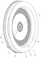
도 1은 플라즈마 처리 챔버 내에서 사용하기 위한 다중-판 면판의 등각도이다.
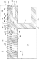
도 2는 다중-판 면판의 단면도이다.
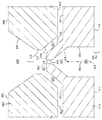
도 3은, 본 개시내용의 제1 실시예에 따른, 도 1의 다중-판 면판의 제1 판과 제2 판 사이의 접합부의 단면도이다.
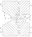
도 4는, 본 개시내용의 제2 실시예에 따른, 도 1의 다중-판 면판의 제1 판과 제2 판 사이의 접합부의 단면도이다.
도 5는, 본 개시내용의 제3 실시예에 따른, 도 1의 다중-판 면판의 제1 판과 제2 판 사이의 접합부의 단면도이다.
이해를 용이하게 하기 위해, 가능한 경우, 도면들에 공통된 동일한 요소들을 지시하는 데에 동일한 참조 번호들이 사용되었다. 일 실시예에 개시된 요소들 및 특징들이 그의 특정 언급 없이 다른 실시예들에 유익하게 통합될 수 있다는 것이 고려된다.
Claims (15)
- 플라즈마 처리 챔버에서 사용하기 위한 다중-판 면판으로서,
복수의 제1 판 개구부들을 갖는 제1 판; 및
제2 판 ― 상기 제2 판은 제1 표면, 반대쪽의 제2 표면 및 상기 제2 판을 통해 연장되는 복수의 제2 판 개구부들을 갖고, 상기 제1 표면은 상기 제1 판에 기계적으로 결합됨 ― 을 포함하고,
상기 제2 판 개구부는, 상기 제1 판 개구부에 유체적으로 결합되도록 구성된 원뿔형 부분을 갖고, 상기 원뿔형 부분은 상기 제2 표면으로부터 상기 원뿔형 부분의 깊이 방향으로 단면이 감소되며,
상기 원뿔형 부분의 표면은 상기 제1 표면과 상기 제2 표면 사이에 보호성 코팅으로 코팅되는, 플라즈마 처리 챔버에서 사용하기 위한 다중-판 면판. - 제1항에 있어서,
상기 제1 판의 내측으로 연장되는 제1 장부촉 핀 홀;
상기 제2 판의 내측으로 연장되는 제2 장부촉 핀 홀; 및
상기 제1 장부촉 핀 홀 및 상기 제2 장부촉 핀 홀의 내측으로 연장되도록 구성된 적어도 하나의 장부촉 핀을 더 포함하는, 플라즈마 처리 챔버에서 사용하기 위한 다중-판 면판. - 제1항에 있어서,
상기 제1 판 및 상기 제2 판에 대해 밀봉하도록 구성된 O-링을 더 포함하는, 플라즈마 처리 챔버에서 사용하기 위한 다중-판 면판. - 제1항에 있어서,
상기 제1 판 내에 배치된 채널을 더 포함하는, 플라즈마 처리 챔버에서 사용하기 위한 다중-판 면판. - 제1항에 있어서,
상기 제2 판 상의 상기 제1 표면 내측으로 형성된 함몰부 ― 상기 함몰부는 상기 제2 판 개구부에 유체적으로 연결됨 ―;
상기 제1 판으로부터 연장되는 돌출부 ― 상기 돌출부는 상기 함몰부의 내측으로 연장됨 ―; 및
상기 돌출부를 통해 연장되고 상기 함몰부와 유체적으로 연결되는 통로 ― 상기 통로는 상기 제1 판 개구부보다 더 작은 단면적을 가짐 ― 를 더 포함하는, 플라즈마 처리 챔버에서 사용하기 위한 다중-판 면판. - 플라즈마 처리 챔버에서 사용하기 위한 다중-판 면판으로서,
복수의 제1 판 개구부들을 갖는 제1 판; 및
제2 판 ― 상기 제2 판은 제1 표면, 반대쪽의 제2 표면 및 상기 제2 판을 통해 연장되는 복수의 제2 판 개구부들을 갖고, 상기 제1 표면은 상기 제1 판에 기계적으로 결합됨 ― 을 포함하고,
상기 제2 판 개구부는, 상기 제1 판 개구부에 유체적으로 결합되도록 구성된 원뿔형 부분을 갖고, 상기 원뿔형 부분은 상기 제2 표면으로부터 상기 원뿔형 부분의 깊이 방향으로 단면이 감소되며,
상기 원뿔형 부분의 표면은 보호성 코팅으로 코팅되는, 플라즈마 처리 챔버에서 사용하기 위한 다중-판 면판. - 제6항에 있어서,
상기 제1 판의 내측으로 연장되는 제1 장부촉 핀 홀;
상기 제2 판의 내측으로 연장되는 제2 장부촉 핀 홀; 및
상기 제1 장부촉 핀 홀 및 상기 제2 장부촉 핀 홀의 내측으로 연장되도록 구성된 적어도 하나의 장부촉 핀을 더 포함하는, 플라즈마 처리 챔버에서 사용하기 위한 다중-판 면판. - 제6항에 있어서,
상기 제1 판 및 상기 제2 판에 대해 밀봉하도록 구성된 O-링을 더 포함하는, 플라즈마 처리 챔버에서 사용하기 위한 다중-판 면판. - 제6항에 있어서,
상기 제1 판 내에 배치된 채널을 더 포함하는, 플라즈마 처리 챔버에서 사용하기 위한 다중-판 면판. - 제6항에 있어서,
상기 제2 판 상의 상기 제1 표면 내측으로 형성된 함몰부 ― 상기 함몰부는 상기 제2 판 개구부에 유체적으로 연결됨 ―;
상기 제1 판으로부터 연장되는 돌출부 ― 상기 돌출부는 상기 함몰부의 내측으로 연장됨 ―; 및
상기 돌출부를 통해 연장되고 상기 함몰부와 유체적으로 연결되는 통로 ― 상기 통로는 상기 제1 판 개구부보다 더 작은 단면적을 가짐 ― 를 더 포함하는, 플라즈마 처리 챔버에서 사용하기 위한 다중-판 면판. - 플라즈마 처리 챔버에서 사용하기 위한 다중-판 면판으로서,
복수의 제1 판 개구부들을 갖는 제1 판; 및
제2 판 ― 상기 제2 판은 제1 표면, 반대쪽의 제2 표면 및 상기 제2 판을 통해 연장되는 복수의 제2 판 개구부들을 갖고, 상기 제1 표면은 상기 제1 판에 기계적으로 결합됨 ― 을 포함하고,
상기 제2 판 개구부는, 상기 제1 판 개구부에 유체적으로 결합되도록 구성된 원뿔형 부분을 갖고,
상기 제1 판은, 상기 제1 판으로부터, 상기 제1 표면의 내측으로 형성된 함몰부 내로 연장되는 돌출부를 갖고, 상기 돌출부는 상기 돌출부를 통해 연장되고 상기 함몰부에 유체적으로 연결된 통로를 가지며 상기 함몰부는 상기 제2 판 개구부에 유체적으로 연결되는, 플라즈마 처리 챔버에서 사용하기 위한 다중-판 면판. - 제11항에 있어서,
상기 제1 판의 내측으로 연장되는 제1 장부촉 핀 홀;
상기 제2 판의 내측으로 연장되는 제2 장부촉 핀 홀; 및
상기 제1 장부촉 핀 홀 및 상기 제2 장부촉 핀 홀의 내측으로 연장되도록 구성된 적어도 하나의 장부촉 핀을 더 포함하는, 플라즈마 처리 챔버에서 사용하기 위한 다중-판 면판. - 제11항에 있어서,
상기 제1 판 및 상기 제2 판에 대해 밀봉하도록 구성된 O-링을 더 포함하는, 플라즈마 처리 챔버에서 사용하기 위한 다중-판 면판. - 제11항에 있어서,
상기 제1 판 내에 배치된 채널을 더 포함하는, 플라즈마 처리 챔버에서 사용하기 위한 다중-판 면판. - 제11항에 있어서, 상기 통로는 상기 제1 판 개구부보다 더 작은 단면적을 갖는, 플라즈마 처리 챔버에서 사용하기 위한 다중-판 면판.
Priority Applications (1)
| Application Number | Priority Date | Filing Date | Title |
|---|---|---|---|
| KR1020227001345A KR102404123B1 (ko) | 2017-08-08 | 2018-08-06 | 처리 챔버를 위한 다중-판 면판 |
Applications Claiming Priority (3)
| Application Number | Priority Date | Filing Date | Title |
|---|---|---|---|
| US15/671,909 | 2017-08-08 | ||
| US15/671,909 US10811232B2 (en) | 2017-08-08 | 2017-08-08 | Multi-plate faceplate for a processing chamber |
| PCT/US2018/045424 WO2019032468A1 (en) | 2017-08-08 | 2018-08-06 | MULTI-PLATE FRONT TRAY FOR A TREATMENT CHAMBER |
Related Child Applications (1)
| Application Number | Title | Priority Date | Filing Date |
|---|---|---|---|
| KR1020227001345A Division KR102404123B1 (ko) | 2017-08-08 | 2018-08-06 | 처리 챔버를 위한 다중-판 면판 |
Publications (2)
| Publication Number | Publication Date |
|---|---|
| KR20200029056A true KR20200029056A (ko) | 2020-03-17 |
| KR102352745B1 KR102352745B1 (ko) | 2022-01-19 |
Family
ID=65271816
Family Applications (2)
| Application Number | Title | Priority Date | Filing Date |
|---|---|---|---|
| KR1020227001345A Active KR102404123B1 (ko) | 2017-08-08 | 2018-08-06 | 처리 챔버를 위한 다중-판 면판 |
| KR1020207006751A Active KR102352745B1 (ko) | 2017-08-08 | 2018-08-06 | 처리 챔버를 위한 다중-판 면판 |
Family Applications Before (1)
| Application Number | Title | Priority Date | Filing Date |
|---|---|---|---|
| KR1020227001345A Active KR102404123B1 (ko) | 2017-08-08 | 2018-08-06 | 처리 챔버를 위한 다중-판 면판 |
Country Status (5)
| Country | Link |
|---|---|
| US (1) | US10811232B2 (ko) |
| JP (1) | JP6947911B2 (ko) |
| KR (2) | KR102404123B1 (ko) |
| CN (2) | CN110753994B (ko) |
| WO (1) | WO2019032468A1 (ko) |
Families Citing this family (16)
| Publication number | Priority date | Publication date | Assignee | Title |
|---|---|---|---|---|
| USD868124S1 (en) | 2017-12-11 | 2019-11-26 | Applied Materials, Inc. | Target profile for a physical vapor deposition chamber target |
| US11232874B2 (en) * | 2017-12-18 | 2022-01-25 | Ge-Hitachi Nuclear Energy Americas Llc | Multiple-path flow restrictor nozzle |
| USD929599S1 (en) * | 2018-10-29 | 2021-08-31 | Custom Molded Products, Llc | Spa jet |
| USD908645S1 (en) * | 2019-08-26 | 2021-01-26 | Applied Materials, Inc. | Sputtering target for a physical vapor deposition chamber |
| USD937329S1 (en) | 2020-03-23 | 2021-11-30 | Applied Materials, Inc. | Sputter target for a physical vapor deposition chamber |
| WO2021262482A1 (en) * | 2020-06-23 | 2021-12-30 | Lam Research Corporation | Sealing surfaces of components used in plasma etching tools using atomic layer deposition |
| WO2022002349A1 (en) * | 2020-06-29 | 2022-01-06 | Applied Materials, Inc. | Nozzle assembly, evaporation source, deposition system and method for depositing an evaporated material onto a substrate |
| USD940765S1 (en) | 2020-12-02 | 2022-01-11 | Applied Materials, Inc. | Target profile for a physical vapor deposition chamber target |
| US11425287B2 (en) * | 2021-01-12 | 2022-08-23 | GM Global Technology Operations LLC | Apparatus for protecting a camera from foreign debris contamination |
| USD1072774S1 (en) | 2021-02-06 | 2025-04-29 | Applied Materials, Inc. | Target profile for a physical vapor deposition chamber target |
| USD1007449S1 (en) | 2021-05-07 | 2023-12-12 | Applied Materials, Inc. | Target profile for a physical vapor deposition chamber target |
| JP7494244B2 (ja) * | 2021-06-02 | 2024-06-03 | 東京エレクトロン株式会社 | シャワーヘッド、電極ユニット、ガス供給ユニット、基板処理装置及び基板処理システム |
| USD1038901S1 (en) | 2022-01-12 | 2024-08-13 | Applied Materials, Inc. | Collimator for a physical vapor deposition chamber |
| US12340980B2 (en) | 2022-04-01 | 2025-06-24 | Applied Materials, Inc. | Plasma showerhead with improved uniformity |
| USD1053230S1 (en) | 2022-05-19 | 2024-12-03 | Applied Materials, Inc. | Sputter target for a physical vapor deposition chamber |
| US20250037978A1 (en) * | 2023-07-24 | 2025-01-30 | Applied Materials, Inc. | Gas distribution assemblies for semiconductor devices |
Citations (4)
| Publication number | Priority date | Publication date | Assignee | Title |
|---|---|---|---|---|
| JP2010067588A (ja) * | 2008-09-11 | 2010-03-25 | Advanced Display Process Engineering Co Ltd | プラズマ処理装置 |
| KR20100048991A (ko) * | 2007-06-13 | 2010-05-11 | 램 리써치 코포레이션 | 열 도전성 개스킷 및 o-링을 이용한 전극 어셈블리 및 플라즈마 프로세싱 챔버 |
| JP2011154973A (ja) * | 2010-01-28 | 2011-08-11 | Mitsubishi Electric Corp | プラズマ処理装置及びプラズマ処理方法 |
| US20120247673A1 (en) * | 2011-03-31 | 2012-10-04 | Tokyo Electron Limited | Electrode having gas discharge function and plasma processing apparatus |
Family Cites Families (14)
| Publication number | Priority date | Publication date | Assignee | Title |
|---|---|---|---|---|
| US4262631A (en) * | 1979-10-01 | 1981-04-21 | Kubacki Ronald M | Thin film deposition apparatus using an RF glow discharge |
| JPS59128281A (ja) * | 1982-12-29 | 1984-07-24 | 信越化学工業株式会社 | 炭化けい素被覆物の製造方法 |
| JPH07111957B2 (ja) * | 1984-03-28 | 1995-11-29 | 圭弘 浜川 | 半導体の製法 |
| US4759947A (en) * | 1984-10-08 | 1988-07-26 | Canon Kabushiki Kaisha | Method for forming deposition film using Si compound and active species from carbon and halogen compound |
| JP3468859B2 (ja) * | 1994-08-16 | 2003-11-17 | 富士通株式会社 | 気相処理装置及び気相処理方法 |
| US6969489B2 (en) * | 2001-08-24 | 2005-11-29 | Cytoplex Biosciences | Micro array for high throughout screening |
| US7270713B2 (en) * | 2003-01-07 | 2007-09-18 | Applied Materials, Inc. | Tunable gas distribution plate assembly |
| CN100375246C (zh) | 2003-03-06 | 2008-03-12 | 积水化学工业株式会社 | 等离子加工装置 |
| US20050241579A1 (en) * | 2004-04-30 | 2005-11-03 | Russell Kidd | Face shield to improve uniformity of blanket CVD processes |
| US7807222B2 (en) * | 2007-09-17 | 2010-10-05 | Asm International N.V. | Semiconductor processing parts having apertures with deposited coatings and methods for forming the same |
| JP6338462B2 (ja) * | 2013-09-11 | 2018-06-06 | 東京エレクトロン株式会社 | プラズマ処理装置 |
| US9484190B2 (en) | 2014-01-25 | 2016-11-01 | Yuri Glukhoy | Showerhead-cooler system of a semiconductor-processing chamber for semiconductor wafers of large area |
| US9911579B2 (en) | 2014-07-03 | 2018-03-06 | Applied Materials, Inc. | Showerhead having a detachable high resistivity gas distribution plate |
| KR101588265B1 (ko) | 2014-08-05 | 2016-01-28 | (주)동원파츠 | 노즐부재 및 이에 의한 가스 디스트리뷰터의 제조방법 |
-
2017
- 2017-08-08 US US15/671,909 patent/US10811232B2/en active Active
-
2018
- 2018-08-06 KR KR1020227001345A patent/KR102404123B1/ko active Active
- 2018-08-06 JP JP2020505779A patent/JP6947911B2/ja active Active
- 2018-08-06 CN CN201880040098.XA patent/CN110753994B/zh active Active
- 2018-08-06 CN CN202310316256.2A patent/CN116313724A/zh active Pending
- 2018-08-06 WO PCT/US2018/045424 patent/WO2019032468A1/en not_active Ceased
- 2018-08-06 KR KR1020207006751A patent/KR102352745B1/ko active Active
Patent Citations (4)
| Publication number | Priority date | Publication date | Assignee | Title |
|---|---|---|---|---|
| KR20100048991A (ko) * | 2007-06-13 | 2010-05-11 | 램 리써치 코포레이션 | 열 도전성 개스킷 및 o-링을 이용한 전극 어셈블리 및 플라즈마 프로세싱 챔버 |
| JP2010067588A (ja) * | 2008-09-11 | 2010-03-25 | Advanced Display Process Engineering Co Ltd | プラズマ処理装置 |
| JP2011154973A (ja) * | 2010-01-28 | 2011-08-11 | Mitsubishi Electric Corp | プラズマ処理装置及びプラズマ処理方法 |
| US20120247673A1 (en) * | 2011-03-31 | 2012-10-04 | Tokyo Electron Limited | Electrode having gas discharge function and plasma processing apparatus |
Also Published As
| Publication number | Publication date |
|---|---|
| KR20220010071A (ko) | 2022-01-25 |
| CN110753994A (zh) | 2020-02-04 |
| CN116313724A (zh) | 2023-06-23 |
| WO2019032468A1 (en) | 2019-02-14 |
| KR102404123B1 (ko) | 2022-05-31 |
| CN110753994B (zh) | 2023-05-23 |
| JP2020530654A (ja) | 2020-10-22 |
| US10811232B2 (en) | 2020-10-20 |
| JP6947911B2 (ja) | 2021-10-13 |
| KR102352745B1 (ko) | 2022-01-19 |
| US20190051499A1 (en) | 2019-02-14 |
Similar Documents
| Publication | Publication Date | Title |
|---|---|---|
| KR102352745B1 (ko) | 처리 챔버를 위한 다중-판 면판 | |
| TWI840450B (zh) | 噴淋頭及氣體處理裝置 | |
| JP6088493B2 (ja) | プラズマエッチングリアクタのセラミックシャワーヘッドのためのガス分配システム | |
| KR102390323B1 (ko) | 플라즈마 프로세싱 챔버를 위한 플라즈마 스크린 | |
| JP6868616B2 (ja) | 背面でのプラズマ点火が低減されたシャワーヘッド | |
| US5597439A (en) | Process gas inlet and distribution passages | |
| JP5891300B2 (ja) | 誘導結合プラズマエッチングリアクタのためのガス分配シャワーヘッド | |
| TWI428713B (zh) | 高腔室溫度製程及用於光阻剝除及後金屬蝕刻鈍化之腔室設計 | |
| CN103053012B (zh) | 具有双轴向气体注入和排放的等离子体处理室 | |
| KR20180076325A (ko) | 가스 공급 장치, 플라스마 처리 장치 및 가스 공급 장치의 제조 방법 | |
| KR20210013634A (ko) | 프로세싱 챔버 내에서의 퍼징 및 플라스마 억제를 위한 방법 및 장치 | |
| US11348763B2 (en) | Corrosion-resistant structure for a gas delivery system in a plasma processing apparatus | |
| JP2009111359A (ja) | 原子層堆積チャンバ及び構成部品 | |
| JP2014515561A5 (ko) | ||
| KR102920695B1 (ko) | 열적 균일 증착 스테이션 | |
| KR101941488B1 (ko) | 샤워 헤드 유닛 및 이를 가지는 기판 처리 장치 | |
| CN108022821B (zh) | 等离子体处理装置及气体通道的耐腐蚀防护方法 | |
| EP1401013B1 (en) | Plasma processing device | |
| TW202105512A (zh) | 電漿處理裝置 | |
| US11944988B2 (en) | Multi-zone showerhead | |
| TWI777258B (zh) | 耐腐蝕氣體輸送部件及其等離子體處理裝置 | |
| JP2019075516A (ja) | プラズマ処理装置及びガス流路が形成される部材 | |
| WO2024155500A1 (en) | Baffle for providing uniform process gas flow on substrate and around pedestal | |
| KR20250139874A (ko) | 에지 가스 유입 장치 및 플라즈마 에칭 시스템 |
Legal Events
| Date | Code | Title | Description |
|---|---|---|---|
| A201 | Request for examination | ||
| PA0105 | International application |
St.27 status event code: A-0-1-A10-A15-nap-PA0105 |
|
| PA0201 | Request for examination |
St.27 status event code: A-1-2-D10-D11-exm-PA0201 |
|
| PG1501 | Laying open of application |
St.27 status event code: A-1-1-Q10-Q12-nap-PG1501 |
|
| E902 | Notification of reason for refusal | ||
| PE0902 | Notice of grounds for rejection |
St.27 status event code: A-1-2-D10-D21-exm-PE0902 |
|
| P11-X000 | Amendment of application requested |
St.27 status event code: A-2-2-P10-P11-nap-X000 |
|
| P13-X000 | Application amended |
St.27 status event code: A-2-2-P10-P13-nap-X000 |
|
| E701 | Decision to grant or registration of patent right | ||
| PE0701 | Decision of registration |
St.27 status event code: A-1-2-D10-D22-exm-PE0701 |
|
| A107 | Divisional application of patent | ||
| GRNT | Written decision to grant | ||
| PA0104 | Divisional application for international application |
St.27 status event code: A-0-1-A10-A18-div-PA0104 St.27 status event code: A-0-1-A10-A16-div-PA0104 |
|
| PR0701 | Registration of establishment |
St.27 status event code: A-2-4-F10-F11-exm-PR0701 |
|
| PR1002 | Payment of registration fee |
St.27 status event code: A-2-2-U10-U12-oth-PR1002 Fee payment year number: 1 |
|
| PG1601 | Publication of registration |
St.27 status event code: A-4-4-Q10-Q13-nap-PG1601 |
|
| PR1001 | Payment of annual fee |
St.27 status event code: A-4-4-U10-U11-oth-PR1001 Fee payment year number: 4 |
|
| PR1001 | Payment of annual fee |
St.27 status event code: A-4-4-U10-U11-oth-PR1001 Fee payment year number: 5 |
|
| U11 | Full renewal or maintenance fee paid |
Free format text: ST27 STATUS EVENT CODE: A-4-4-U10-U11-OTH-PR1001 (AS PROVIDED BY THE NATIONAL OFFICE) Year of fee payment: 5 |
|
| P22-X000 | Classification modified |
St.27 status event code: A-4-4-P10-P22-nap-X000 |