KR20200030963A - 전력 증폭기 - Google Patents
전력 증폭기 Download PDFInfo
- Publication number
- KR20200030963A KR20200030963A KR1020180109833A KR20180109833A KR20200030963A KR 20200030963 A KR20200030963 A KR 20200030963A KR 1020180109833 A KR1020180109833 A KR 1020180109833A KR 20180109833 A KR20180109833 A KR 20180109833A KR 20200030963 A KR20200030963 A KR 20200030963A
- Authority
- KR
- South Korea
- Prior art keywords
- terminal
- transistor
- voltage
- power
- input
- Prior art date
- Legal status (The legal status is an assumption and is not a legal conclusion. Google has not performed a legal analysis and makes no representation as to the accuracy of the status listed.)
- Granted
Links
Images


Classifications
-
- H—ELECTRICITY
- H03—ELECTRONIC CIRCUITRY
- H03F—AMPLIFIERS
- H03F1/00—Details of amplifiers with only discharge tubes, only semiconductor devices or only unspecified devices as amplifying elements
- H03F1/02—Modifications of amplifiers to raise the efficiency, e.g. gliding Class A stages, use of an auxiliary oscillation
- H03F1/0205—Modifications of amplifiers to raise the efficiency, e.g. gliding Class A stages, use of an auxiliary oscillation in transistor amplifiers
- H03F1/0211—Modifications of amplifiers to raise the efficiency, e.g. gliding Class A stages, use of an auxiliary oscillation in transistor amplifiers with control of the supply voltage or current
- H03F1/0216—Continuous control
- H03F1/0222—Continuous control by using a signal derived from the input signal
- H03F1/0227—Continuous control by using a signal derived from the input signal using supply converters
-
- H—ELECTRICITY
- H03—ELECTRONIC CIRCUITRY
- H03F—AMPLIFIERS
- H03F3/00—Amplifiers with only discharge tubes or only semiconductor devices as amplifying elements
- H03F3/04—Amplifiers with only discharge tubes or only semiconductor devices as amplifying elements with semiconductor devices only
- H03F3/10—Amplifiers with only discharge tubes or only semiconductor devices as amplifying elements with semiconductor devices only with diodes
Landscapes
- Engineering & Computer Science (AREA)
- Power Engineering (AREA)
- Amplifiers (AREA)
Abstract
Description
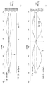
도 2는 도 1의 구성을 적용한 밀리미터파 차동 전력증폭기의 개념도이다.
도 3은 본 발명의 실시 예에 따른 바이어스 회로를 포함한 1단의 증폭기 회로를 나타낸 도면이다.
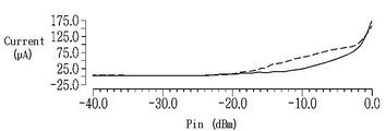
도 4는 본 발명의 실시 예에 따른 바이어스 회로에서 제3 증폭기로 흐르는 전류와 인버터 회로 사이의 저항에 흐르는 전류를 나타낸 도면이다.
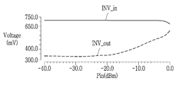
도 5는 도 3에 도시된 인버터 회로의 입력 신호와 출력 신호의 DC 전압 값을 모니터링한 결과를 나타낸 도면이다.
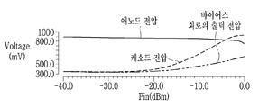
도 6은 도 3에 도시된 다이오드의 애노드 전압과 캐소드 전압, 그리고 바이어스 회로의 출력 전압을 나타낸 도면이다.
도 7은 도 3에 도시된 다이오드에서 흐르는 전류를 도시한 도면이다.
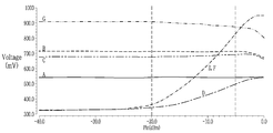
도 8은 입력 신호 전력에 따른 다이오드의 전압 파형과 바이어스 회로의 최종 전압 파형을 나타낸 도면이다.
도 9는 본 발명의 실시 예에 따른 바이어스 회로의 각 노드의 전압 값을 나타낸 도면이다.
도 10은 본 발명의 실시 예에 따른 바이어스 회로를 적용하기 전에 3단의 전력 증폭기의 입력 전력에 따른 이득 특성을 나타낸 도면이다.
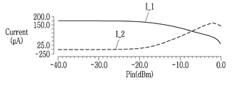
도 11은 본 발명의 실시 예에 따른 바이어스 회로를 적용하기 전에 3단의 전력 증폭기의 효율 및 소모 전류를 나타낸 도면이다.
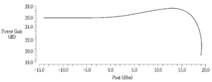
도 12는 본 발명의 실시 예에 따른 바이어스 회로를 적용한 3단의 전력 증폭기의 입력 전력에 따른 이득 특성을 나타낸 도면이다.
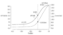
도 13은 본 발명의 실시 예에 따른 바이어스 회로를 적용한 3단의 전력 증폭기의 효율 및 소모 전류를 나타낸 도면이다.
도 14는 본 발명의 다른 실시 예에 따른 바이어스 회로를 나타낸 도면이다.
도 15는 도 14에 도시된 바이어스 회로를 적용한 전력 증폭기의 효율을 나타낸 도면이다.
도 16은 본 발명의 또 다른 실시 예에 따른 바이어스 회로를 나타낸 도면이다.
Claims (1)
- 공통 소스 구조로 이루어진 복수의 증폭 회로, 그리고
상기 복수의 증폭 회로 중 적어도 하나의 증폭 회로에 바이어스 전압을 인가하는 바이어스 회로를 포함하고,
상기 바이어스 회로는
외부로부터 인가되는 전압에 의해 턴온되고, 제1단이 전원 전압을 인가하는 전원단에 연결되고 제2단이 접지단에 연결되는 제1 트랜지스터,
상기 전원단과 상기 제1 트랜지스터의 제1단 사이에 직렬로 연결되는 제1 및 제2 저항,
상기 제1 및 제2 저항 사이의 노드에 애노드가 연결되고 캐소드가 상기 적어도 하나의 증폭 회로의 입력단에 연결되는 제1 다이오드,
제1단이 상기 제1 다이오드의 캐소드에 연결되어 있는 제3 저항,
상기 제3 저항의 제2단에 출력단이 연결되고 상기 제1 트랜지스터의 제2단에 입력단이 연결되는 인버터 회로, 그리고
상기 인버터 회로의 입력단과 출력단 사이에 직렬로 연결되어 있는 제2 트랜지스터와 제4 저항을 포함하는 전력 증폭기.
Priority Applications (1)
| Application Number | Priority Date | Filing Date | Title |
|---|---|---|---|
| KR1020180109833A KR102593564B1 (ko) | 2018-09-13 | 2018-09-13 | 전력 증폭기 |
Applications Claiming Priority (1)
| Application Number | Priority Date | Filing Date | Title |
|---|---|---|---|
| KR1020180109833A KR102593564B1 (ko) | 2018-09-13 | 2018-09-13 | 전력 증폭기 |
Publications (2)
| Publication Number | Publication Date |
|---|---|
| KR20200030963A true KR20200030963A (ko) | 2020-03-23 |
| KR102593564B1 KR102593564B1 (ko) | 2023-10-25 |
Family
ID=69998711
Family Applications (1)
| Application Number | Title | Priority Date | Filing Date |
|---|---|---|---|
| KR1020180109833A Active KR102593564B1 (ko) | 2018-09-13 | 2018-09-13 | 전력 증폭기 |
Country Status (1)
| Country | Link |
|---|---|
| KR (1) | KR102593564B1 (ko) |
Citations (3)
| Publication number | Priority date | Publication date | Assignee | Title |
|---|---|---|---|---|
| JPS6181009A (ja) * | 1984-09-28 | 1986-04-24 | Matsushita Electric Ind Co Ltd | トランジスタバイアス装置 |
| JPS62128204A (ja) * | 1985-11-28 | 1987-06-10 | Mitsubishi Electric Corp | 定電流回路 |
| US20160261235A1 (en) * | 2015-03-06 | 2016-09-08 | RF Micro Devices. Inc. | Multistage differential power amplifier having interstage power limiter |
-
2018
- 2018-09-13 KR KR1020180109833A patent/KR102593564B1/ko active Active
Patent Citations (3)
| Publication number | Priority date | Publication date | Assignee | Title |
|---|---|---|---|---|
| JPS6181009A (ja) * | 1984-09-28 | 1986-04-24 | Matsushita Electric Ind Co Ltd | トランジスタバイアス装置 |
| JPS62128204A (ja) * | 1985-11-28 | 1987-06-10 | Mitsubishi Electric Corp | 定電流回路 |
| US20160261235A1 (en) * | 2015-03-06 | 2016-09-08 | RF Micro Devices. Inc. | Multistage differential power amplifier having interstage power limiter |
Also Published As
| Publication number | Publication date |
|---|---|
| KR102593564B1 (ko) | 2023-10-25 |
Similar Documents
| Publication | Publication Date | Title |
|---|---|---|
| US10491168B2 (en) | Power amplification circuit | |
| US5942946A (en) | RF power amplifier with high efficiency and a wide range of gain control | |
| CN100555844C (zh) | 射频放大器电路及其操作方法 | |
| US8497736B1 (en) | Direct DC coupled push-pull BJT driver for power amplifier with built-in gain and bias current signal dependent expansion | |
| US11323081B2 (en) | Power amplifier circuit | |
| US20080036538A1 (en) | Rail-to-rail class ab amplifier | |
| US7852136B2 (en) | Bias network | |
| US20180159484A1 (en) | Linear cmos pa with low quiescent current and boosted maximum linear output power | |
| US9722546B2 (en) | Bias circuit for low quiescent current amplifier | |
| US11201594B2 (en) | Cascode amplifier circuit | |
| US10044330B2 (en) | Power amplifier module | |
| US10476454B2 (en) | Power amplifier module | |
| JP2017098892A (ja) | 電力増幅モジュール | |
| US6897732B2 (en) | Amplifier | |
| US10855239B2 (en) | Amplifier class AB output stage | |
| KR101801938B1 (ko) | 전력 증폭기 | |
| CN105207633B (zh) | 功率放大器 | |
| WO2023090064A1 (ja) | リミッタ回路、整合回路及び電力増幅回路 | |
| US8736376B2 (en) | Power amplifier module having bias circuit | |
| US7019588B2 (en) | Method to dynamically control the quiescent current of an operational amplifier arrangement and operational amplifier arrangement performing this method | |
| KR102593564B1 (ko) | 전력 증폭기 | |
| KR101891619B1 (ko) | 질화갈륨 집적회로 증폭기의 선형화 바이어스 회로 기술 | |
| JP2020017801A (ja) | 増幅器 | |
| US7456692B2 (en) | Gain variable amplifier | |
| CN115225040A (zh) | 功率放大电路 |
Legal Events
| Date | Code | Title | Description |
|---|---|---|---|
| PA0109 | Patent application |
St.27 status event code: A-0-1-A10-A12-nap-PA0109 |
|
| PG1501 | Laying open of application |
St.27 status event code: A-1-1-Q10-Q12-nap-PG1501 |
|
| A201 | Request for examination | ||
| P11-X000 | Amendment of application requested |
St.27 status event code: A-2-2-P10-P11-nap-X000 |
|
| P13-X000 | Application amended |
St.27 status event code: A-2-2-P10-P13-nap-X000 |
|
| PA0201 | Request for examination |
St.27 status event code: A-1-2-D10-D11-exm-PA0201 |
|
| R17-X000 | Change to representative recorded |
St.27 status event code: A-3-3-R10-R17-oth-X000 |
|
| D13-X000 | Search requested |
St.27 status event code: A-1-2-D10-D13-srh-X000 |
|
| D14-X000 | Search report completed |
St.27 status event code: A-1-2-D10-D14-srh-X000 |
|
| E902 | Notification of reason for refusal | ||
| PE0902 | Notice of grounds for rejection |
St.27 status event code: A-1-2-D10-D21-exm-PE0902 |
|
| E13-X000 | Pre-grant limitation requested |
St.27 status event code: A-2-3-E10-E13-lim-X000 |
|
| P11-X000 | Amendment of application requested |
St.27 status event code: A-2-2-P10-P11-nap-X000 |
|
| P13-X000 | Application amended |
St.27 status event code: A-2-2-P10-P13-nap-X000 |
|
| E701 | Decision to grant or registration of patent right | ||
| PE0701 | Decision of registration |
St.27 status event code: A-1-2-D10-D22-exm-PE0701 |
|
| PR0701 | Registration of establishment |
St.27 status event code: A-2-4-F10-F11-exm-PR0701 |
|
| PR1002 | Payment of registration fee |
St.27 status event code: A-2-2-U10-U11-oth-PR1002 Fee payment year number: 1 |
|
| PG1601 | Publication of registration |
St.27 status event code: A-4-4-Q10-Q13-nap-PG1601 |