KR20200032361A - Mems 디바이스 - Google Patents
Mems 디바이스 Download PDFInfo
- Publication number
- KR20200032361A KR20200032361A KR1020180111289A KR20180111289A KR20200032361A KR 20200032361 A KR20200032361 A KR 20200032361A KR 1020180111289 A KR1020180111289 A KR 1020180111289A KR 20180111289 A KR20180111289 A KR 20180111289A KR 20200032361 A KR20200032361 A KR 20200032361A
- Authority
- KR
- South Korea
- Prior art keywords
- mems device
- cap
- bonding layer
- cavity
- preventing portion
- Prior art date
- Legal status (The legal status is an assumption and is not a legal conclusion. Google has not performed a legal analysis and makes no representation as to the accuracy of the status listed.)
- Withdrawn
Links
Images




Classifications
-
- B—PERFORMING OPERATIONS; TRANSPORTING
- B81—MICROSTRUCTURAL TECHNOLOGY
- B81B—MICROSTRUCTURAL DEVICES OR SYSTEMS, e.g. MICROMECHANICAL DEVICES
- B81B7/00—Microstructural systems ; Auxiliary parts of microstructural devices or systems
- B81B7/0032—Packages or encapsulation
- B81B7/0035—Packages or encapsulation for maintaining a controlled atmosphere inside of the chamber containing the MEMS
-
- B—PERFORMING OPERATIONS; TRANSPORTING
- B81—MICROSTRUCTURAL TECHNOLOGY
- B81B—MICROSTRUCTURAL DEVICES OR SYSTEMS, e.g. MICROMECHANICAL DEVICES
- B81B7/00—Microstructural systems ; Auxiliary parts of microstructural devices or systems
- B81B7/0032—Packages or encapsulation
- B81B7/0061—Packages or encapsulation suitable for fluid transfer from the MEMS out of the package or vice versa, e.g. transfer of liquid, gas, sound
-
- B—PERFORMING OPERATIONS; TRANSPORTING
- B81—MICROSTRUCTURAL TECHNOLOGY
- B81B—MICROSTRUCTURAL DEVICES OR SYSTEMS, e.g. MICROMECHANICAL DEVICES
- B81B7/00—Microstructural systems ; Auxiliary parts of microstructural devices or systems
- B81B7/0032—Packages or encapsulation
- B81B7/0077—Other packages not provided for in groups B81B7/0035 - B81B7/0074
-
- B—PERFORMING OPERATIONS; TRANSPORTING
- B81—MICROSTRUCTURAL TECHNOLOGY
- B81C—PROCESSES OR APPARATUS SPECIALLY ADAPTED FOR THE MANUFACTURE OR TREATMENT OF MICROSTRUCTURAL DEVICES OR SYSTEMS
- B81C1/00—Manufacture or treatment of devices or systems in or on a substrate
- B81C1/00015—Manufacture or treatment of devices or systems in or on a substrate for manufacturing microsystems
- B81C1/00261—Processes for packaging MEMS devices
- B81C1/00269—Bonding of solid lids or wafers to the substrate
-
- B—PERFORMING OPERATIONS; TRANSPORTING
- B81—MICROSTRUCTURAL TECHNOLOGY
- B81B—MICROSTRUCTURAL DEVICES OR SYSTEMS, e.g. MICROMECHANICAL DEVICES
- B81B7/00—Microstructural systems ; Auxiliary parts of microstructural devices or systems
- B81B7/02—Microstructural systems ; Auxiliary parts of microstructural devices or systems containing distinct electrical or optical devices of particular relevance for their function, e.g. microelectro-mechanical systems [MEMS]
-
- B—PERFORMING OPERATIONS; TRANSPORTING
- B81—MICROSTRUCTURAL TECHNOLOGY
- B81C—PROCESSES OR APPARATUS SPECIALLY ADAPTED FOR THE MANUFACTURE OR TREATMENT OF MICROSTRUCTURAL DEVICES OR SYSTEMS
- B81C1/00—Manufacture or treatment of devices or systems in or on a substrate
- B81C1/00015—Manufacture or treatment of devices or systems in or on a substrate for manufacturing microsystems
- B81C1/00261—Processes for packaging MEMS devices
- B81C1/00309—Processes for packaging MEMS devices suitable for fluid transfer from the MEMS out of the package or vice versa, e.g. transfer of liquid, gas, sound
-
- B—PERFORMING OPERATIONS; TRANSPORTING
- B81—MICROSTRUCTURAL TECHNOLOGY
- B81B—MICROSTRUCTURAL DEVICES OR SYSTEMS, e.g. MICROMECHANICAL DEVICES
- B81B2203/00—Basic microelectromechanical structures
- B81B2203/03—Static structures
- B81B2203/0315—Cavities
-
- B—PERFORMING OPERATIONS; TRANSPORTING
- B81—MICROSTRUCTURAL TECHNOLOGY
- B81B—MICROSTRUCTURAL DEVICES OR SYSTEMS, e.g. MICROMECHANICAL DEVICES
- B81B2203/00—Basic microelectromechanical structures
- B81B2203/03—Static structures
- B81B2203/0323—Grooves
- B81B2203/033—Trenches
-
- B—PERFORMING OPERATIONS; TRANSPORTING
- B81—MICROSTRUCTURAL TECHNOLOGY
- B81B—MICROSTRUCTURAL DEVICES OR SYSTEMS, e.g. MICROMECHANICAL DEVICES
- B81B2207/00—Microstructural systems or auxiliary parts thereof
- B81B2207/09—Packages
-
- B—PERFORMING OPERATIONS; TRANSPORTING
- B81—MICROSTRUCTURAL TECHNOLOGY
- B81C—PROCESSES OR APPARATUS SPECIALLY ADAPTED FOR THE MANUFACTURE OR TREATMENT OF MICROSTRUCTURAL DEVICES OR SYSTEMS
- B81C2203/00—Forming microstructural systems
- B81C2203/01—Packaging MEMS
- B81C2203/0109—Bonding an individual cap on the substrate
Landscapes
- Engineering & Computer Science (AREA)
- Microelectronics & Electronic Packaging (AREA)
- Manufacturing & Machinery (AREA)
- Computer Hardware Design (AREA)
- Micromachines (AREA)
Abstract
Description
도 2는 본 발명의 제1 실시예에 따른 MEMS 디바이스의 분해 단면도이다.
도 3 내지 도 7은 본 발명의 제1 실시예에 따른 MEMS 디바이스에 구비되는 캡의 제1 제조방법을 설명하기 위한 공정 흐름도이다.
도 8 내지 도 10는 본 발명의 제1 실시예에 따른 MEMS 디바이스에 구비되는 캡의 제2 제조방법을 설명하기 위한 공정 흐름도이다.
120 : 기판
140 : MEMS 소자부
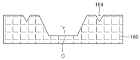
160 : 캡
180 : 확산방지층
Claims (10)
- 기판;
기판의 일면에 배치되는 MEMS 소자부;
상기 MEMS 소자부에 대향 배치되는 캐비티가 형성되는 캡; 및
상기 캡부재의 적어도 일부에 형성되는 확산방지층;
을 포함하며,
상기 캡과 상기 기판 중 적어도 하나에는 상기 캐비티의 외측에 배치되는 접합층을 구비하며,
상기 캡에는 상기 접합층과 상기 캐비티 사이에 배치되며 단면이 'V'자 형상을 가지는 퍼짐방지부가 형성되는 MEMS 디바이스.
- 제1항에 있어서,
상기 확산방지층은 적어도 상기 퍼짐방지부 내부 및 상기 접합층의 주위에 형성되는 MEMS 디바이스.
- 제1항에 있어서,
상기 캡은 실리콘을 함유하는 재질로 이루어지며, 상기 접합층은 금속 재질로 이루어지는 MEMS 디바이스.
- 제3항에 있어서,
상기 접합층은 금(Au), 주석(Sn), 크롬(Cr) 및 티탄(Ti), 알루미늄(Al) 중 적어도 하나를 함유하는 재질로 이루어지는 MEMS 디바이스.
- 제1항에 있어서,
상기 확산방지층은 산화막으로 이루어지는 MEMS 디바이스.
- 제1항에 있어서,
상기 퍼짐방지부는 결정면 (111)에 의하여 50° ~ 60°의 각도를 가지는 경사면을 가지는 MEMS 디바이스.
- 제6항에 있어서,
상기 퍼짐방지부는 결정면 (111)에 의하여 54.74°의 각도를 가지는 경사면을 가지는 MEMS 디바이스.
- 제1항에 있어서,
상기 확산방지층은 상기 캐비티 내를 제외한 부분에 형성되는 MEMS 디바이스.
- 제1항에 있어서,
상기 퍼짐방지부는 상기 캐비티의 형상에 대응되는 띠 형상을 가지는 MEMS 디바이스.
- 제1항에 있어서,
상기 캐비티는 단면이 사각형 형상을 가지는 MEMS 디바이스.
Priority Applications (3)
| Application Number | Priority Date | Filing Date | Title |
|---|---|---|---|
| KR1020180111289A KR20200032361A (ko) | 2018-09-18 | 2018-09-18 | Mems 디바이스 |
| US16/357,588 US10781096B2 (en) | 2018-09-18 | 2019-03-19 | MEMS device |
| CN201910499886.1A CN110902641A (zh) | 2018-09-18 | 2019-06-11 | 微机电系统器件 |
Applications Claiming Priority (1)
| Application Number | Priority Date | Filing Date | Title |
|---|---|---|---|
| KR1020180111289A KR20200032361A (ko) | 2018-09-18 | 2018-09-18 | Mems 디바이스 |
Publications (1)
| Publication Number | Publication Date |
|---|---|
| KR20200032361A true KR20200032361A (ko) | 2020-03-26 |
Family
ID=69772269
Family Applications (1)
| Application Number | Title | Priority Date | Filing Date |
|---|---|---|---|
| KR1020180111289A Withdrawn KR20200032361A (ko) | 2018-09-18 | 2018-09-18 | Mems 디바이스 |
Country Status (3)
| Country | Link |
|---|---|
| US (1) | US10781096B2 (ko) |
| KR (1) | KR20200032361A (ko) |
| CN (1) | CN110902641A (ko) |
Citations (1)
| Publication number | Priority date | Publication date | Assignee | Title |
|---|---|---|---|---|
| KR20170073080A (ko) | 2015-12-18 | 2017-06-28 | 삼성전기주식회사 | 음향 공진기 및 그 제조 방법 |
Family Cites Families (9)
| Publication number | Priority date | Publication date | Assignee | Title |
|---|---|---|---|---|
| JPH10303323A (ja) * | 1997-04-25 | 1998-11-13 | Fukushima Nippon Denki Kk | 半導体集積回路の気密封止パッケージ |
| US20020150129A1 (en) * | 2001-04-16 | 2002-10-17 | Coldren Larry A. | Tunable VCSEL assembly |
| JP2003043312A (ja) | 2001-07-27 | 2003-02-13 | Kyocera Corp | サブマウントおよびそれを用いた光半導体装置ならびにサブマウントの製造方法 |
| JP2003053775A (ja) | 2001-08-15 | 2003-02-26 | Shinko Electric Ind Co Ltd | 樹脂封止用金型及び該金型を用いた半導体装置の製造方法 |
| DE102005053722B4 (de) * | 2005-11-10 | 2007-08-16 | Fraunhofer-Gesellschaft zur Förderung der angewandten Forschung e.V. | Deckelwafer, in der Mikrosystemtechnik einsetzbares Bauelement mit einem solchen Wafer sowie Lötverfahren zum Verbinden entsprechender Bauelement-Teile |
| CN100394623C (zh) * | 2006-04-27 | 2008-06-11 | 矽畿科技股份有限公司 | 光二极管的封装基座结构及其制作方法 |
| CN101459210A (zh) * | 2007-12-14 | 2009-06-17 | 先进开发光电股份有限公司 | 光电元件的封装结构及其制造方法 |
| CN103299410B (zh) * | 2011-01-26 | 2016-01-27 | 株式会社村田制作所 | 电子元器件模块及电子元器件单元 |
| JP6547745B2 (ja) * | 2014-06-27 | 2019-07-24 | ソニー株式会社 | 半導体装置およびその製造方法 |
-
2018
- 2018-09-18 KR KR1020180111289A patent/KR20200032361A/ko not_active Withdrawn
-
2019
- 2019-03-19 US US16/357,588 patent/US10781096B2/en active Active
- 2019-06-11 CN CN201910499886.1A patent/CN110902641A/zh active Pending
Patent Citations (1)
| Publication number | Priority date | Publication date | Assignee | Title |
|---|---|---|---|---|
| KR20170073080A (ko) | 2015-12-18 | 2017-06-28 | 삼성전기주식회사 | 음향 공진기 및 그 제조 방법 |
Also Published As
| Publication number | Publication date |
|---|---|
| US10781096B2 (en) | 2020-09-22 |
| US20200087141A1 (en) | 2020-03-19 |
| CN110902641A (zh) | 2020-03-24 |
Similar Documents
| Publication | Publication Date | Title |
|---|---|---|
| JP5913564B2 (ja) | アウトオブプレーンスペーサが画成する電極 | |
| CN105404059B (zh) | 液晶显示装置及母板 | |
| US20130285175A1 (en) | Micromechanical component and method for manufacturing a micromechanical component | |
| KR20140033211A (ko) | 환경에 노출된 부분을 갖는 밀봉 mems 디바이스를 위한 공정 | |
| US9416000B2 (en) | Component including two semiconductor elements, between which at least two hermetically sealed cavities are formed and method for establishing a corresponding bonding connection between two semiconductor elements | |
| JPH08316497A (ja) | 半導体装置の製造方法 | |
| US11724933B2 (en) | Eutectic bonding with AlGe | |
| US9425382B2 (en) | Sensor protective coating | |
| US20080233714A1 (en) | Method for fabricating semiconductor device | |
| US8138025B2 (en) | Microcap wafer bonding method and apparatus | |
| JP2012033718A (ja) | 半導体装置及びその製造方法 | |
| CN104966676A (zh) | 共晶键合方法 | |
| KR20200032361A (ko) | Mems 디바이스 | |
| US9469522B2 (en) | Epi-poly etch stop for out of plane spacer defined electrode | |
| US7977786B2 (en) | Saw debris reduction in MEMS devices | |
| JP2012040677A (ja) | Memsセンサ | |
| JP6891202B2 (ja) | 応力低減レイヤを有する密封されたパッケージ | |
| JP3896780B2 (ja) | 液晶表示装置の製造方法 | |
| US20180257932A1 (en) | Manufacturing method for a micromechanical device including an oblique surface and corresponding micromechanical device | |
| JP6891203B2 (ja) | 応力低減レイヤを有する密封されたパッケージ | |
| JP2000131169A (ja) | 半導体圧力センサおよびその製造方法 | |
| JP2005311065A (ja) | Memsデバイスの製造方法及びmemsデバイスを製造するための接合基板 | |
| CN117735477A (zh) | 一种mems芯片封装结构及制作方法 | |
| JP2008235628A (ja) | 半導体装置 | |
| JPH06324076A (ja) | 半導体加速度センサ |
Legal Events
| Date | Code | Title | Description |
|---|---|---|---|
| PA0109 | Patent application |
Patent event code: PA01091R01D Comment text: Patent Application Patent event date: 20180918 |
|
| PG1501 | Laying open of application | ||
| A201 | Request for examination | ||
| PA0201 | Request for examination |
Patent event code: PA02012R01D Patent event date: 20210830 Comment text: Request for Examination of Application Patent event code: PA02011R01I Patent event date: 20180918 Comment text: Patent Application |
|
| E902 | Notification of reason for refusal | ||
| PE0902 | Notice of grounds for rejection |
Comment text: Notification of reason for refusal Patent event date: 20230118 Patent event code: PE09021S01D |
|
| E90F | Notification of reason for final refusal | ||
| PE0902 | Notice of grounds for rejection |
Comment text: Final Notice of Reason for Refusal Patent event date: 20230718 Patent event code: PE09021S02D |
|
| PC1202 | Submission of document of withdrawal before decision of registration |
Comment text: [Withdrawal of Procedure relating to Patent, etc.] Withdrawal (Abandonment) Patent event code: PC12021R01D Patent event date: 20231128 |
|
| WITB | Written withdrawal of application |