KR20200032527A - 메모리 시스템의 동작 방법 및 메모리 시스템 - Google Patents
메모리 시스템의 동작 방법 및 메모리 시스템 Download PDFInfo
- Publication number
- KR20200032527A KR20200032527A KR1020180111661A KR20180111661A KR20200032527A KR 20200032527 A KR20200032527 A KR 20200032527A KR 1020180111661 A KR1020180111661 A KR 1020180111661A KR 20180111661 A KR20180111661 A KR 20180111661A KR 20200032527 A KR20200032527 A KR 20200032527A
- Authority
- KR
- South Korea
- Prior art keywords
- logical address
- block
- valid data
- blocks
- memory
- Prior art date
- Legal status (The legal status is an assumption and is not a legal conclusion. Google has not performed a legal analysis and makes no representation as to the accuracy of the status listed.)
- Granted
Links
Images




Classifications
-
- G—PHYSICS
- G06—COMPUTING OR CALCULATING; COUNTING
- G06F—ELECTRIC DIGITAL DATA PROCESSING
- G06F3/00—Input arrangements for transferring data to be processed into a form capable of being handled by the computer; Output arrangements for transferring data from processing unit to output unit, e.g. interface arrangements
- G06F3/06—Digital input from, or digital output to, record carriers, e.g. RAID, emulated record carriers or networked record carriers
- G06F3/0601—Interfaces specially adapted for storage systems
- G06F3/0602—Interfaces specially adapted for storage systems specifically adapted to achieve a particular effect
- G06F3/0614—Improving the reliability of storage systems
- G06F3/0619—Improving the reliability of storage systems in relation to data integrity, e.g. data losses, bit errors
-
- G—PHYSICS
- G06—COMPUTING OR CALCULATING; COUNTING
- G06F—ELECTRIC DIGITAL DATA PROCESSING
- G06F12/00—Accessing, addressing or allocating within memory systems or architectures
- G06F12/02—Addressing or allocation; Relocation
- G06F12/0223—User address space allocation, e.g. contiguous or non contiguous base addressing
- G06F12/023—Free address space management
- G06F12/0238—Memory management in non-volatile memory, e.g. resistive RAM or ferroelectric memory
- G06F12/0246—Memory management in non-volatile memory, e.g. resistive RAM or ferroelectric memory in block erasable memory, e.g. flash memory
-
- G—PHYSICS
- G06—COMPUTING OR CALCULATING; COUNTING
- G06F—ELECTRIC DIGITAL DATA PROCESSING
- G06F11/00—Error detection; Error correction; Monitoring
- G06F11/07—Responding to the occurrence of a fault, e.g. fault tolerance
- G06F11/14—Error detection or correction of the data by redundancy in operations
- G06F11/1446—Point-in-time backing up or restoration of persistent data
-
- G—PHYSICS
- G06—COMPUTING OR CALCULATING; COUNTING
- G06F—ELECTRIC DIGITAL DATA PROCESSING
- G06F11/00—Error detection; Error correction; Monitoring
- G06F11/07—Responding to the occurrence of a fault, e.g. fault tolerance
- G06F11/14—Error detection or correction of the data by redundancy in operations
- G06F11/1446—Point-in-time backing up or restoration of persistent data
- G06F11/1448—Management of the data involved in backup or backup restore
-
- G—PHYSICS
- G06—COMPUTING OR CALCULATING; COUNTING
- G06F—ELECTRIC DIGITAL DATA PROCESSING
- G06F11/00—Error detection; Error correction; Monitoring
- G06F11/07—Responding to the occurrence of a fault, e.g. fault tolerance
- G06F11/14—Error detection or correction of the data by redundancy in operations
- G06F11/1446—Point-in-time backing up or restoration of persistent data
- G06F11/1458—Management of the backup or restore process
- G06F11/1464—Management of the backup or restore process for networked environments
-
- G—PHYSICS
- G06—COMPUTING OR CALCULATING; COUNTING
- G06F—ELECTRIC DIGITAL DATA PROCESSING
- G06F12/00—Accessing, addressing or allocating within memory systems or architectures
- G06F12/02—Addressing or allocation; Relocation
- G06F12/0223—User address space allocation, e.g. contiguous or non contiguous base addressing
- G06F12/0292—User address space allocation, e.g. contiguous or non contiguous base addressing using tables or multilevel address translation means
-
- G—PHYSICS
- G06—COMPUTING OR CALCULATING; COUNTING
- G06F—ELECTRIC DIGITAL DATA PROCESSING
- G06F3/00—Input arrangements for transferring data to be processed into a form capable of being handled by the computer; Output arrangements for transferring data from processing unit to output unit, e.g. interface arrangements
- G06F3/06—Digital input from, or digital output to, record carriers, e.g. RAID, emulated record carriers or networked record carriers
- G06F3/0601—Interfaces specially adapted for storage systems
- G06F3/0602—Interfaces specially adapted for storage systems specifically adapted to achieve a particular effect
- G06F3/061—Improving I/O performance
-
- G—PHYSICS
- G06—COMPUTING OR CALCULATING; COUNTING
- G06F—ELECTRIC DIGITAL DATA PROCESSING
- G06F3/00—Input arrangements for transferring data to be processed into a form capable of being handled by the computer; Output arrangements for transferring data from processing unit to output unit, e.g. interface arrangements
- G06F3/06—Digital input from, or digital output to, record carriers, e.g. RAID, emulated record carriers or networked record carriers
- G06F3/0601—Interfaces specially adapted for storage systems
- G06F3/0628—Interfaces specially adapted for storage systems making use of a particular technique
- G06F3/0638—Organizing or formatting or addressing of data
- G06F3/064—Management of blocks
-
- G—PHYSICS
- G06—COMPUTING OR CALCULATING; COUNTING
- G06F—ELECTRIC DIGITAL DATA PROCESSING
- G06F3/00—Input arrangements for transferring data to be processed into a form capable of being handled by the computer; Output arrangements for transferring data from processing unit to output unit, e.g. interface arrangements
- G06F3/06—Digital input from, or digital output to, record carriers, e.g. RAID, emulated record carriers or networked record carriers
- G06F3/0601—Interfaces specially adapted for storage systems
- G06F3/0628—Interfaces specially adapted for storage systems making use of a particular technique
- G06F3/0646—Horizontal data movement in storage systems, i.e. moving data in between storage devices or systems
- G06F3/0647—Migration mechanisms
-
- G—PHYSICS
- G06—COMPUTING OR CALCULATING; COUNTING
- G06F—ELECTRIC DIGITAL DATA PROCESSING
- G06F3/00—Input arrangements for transferring data to be processed into a form capable of being handled by the computer; Output arrangements for transferring data from processing unit to output unit, e.g. interface arrangements
- G06F3/06—Digital input from, or digital output to, record carriers, e.g. RAID, emulated record carriers or networked record carriers
- G06F3/0601—Interfaces specially adapted for storage systems
- G06F3/0668—Interfaces specially adapted for storage systems adopting a particular infrastructure
- G06F3/0671—In-line storage system
- G06F3/0673—Single storage device
- G06F3/0679—Non-volatile semiconductor memory device, e.g. flash memory, one time programmable memory [OTP]
-
- G—PHYSICS
- G06—COMPUTING OR CALCULATING; COUNTING
- G06F—ELECTRIC DIGITAL DATA PROCESSING
- G06F2212/00—Indexing scheme relating to accessing, addressing or allocation within memory systems or architectures
- G06F2212/10—Providing a specific technical effect
- G06F2212/1008—Correctness of operation, e.g. memory ordering
-
- G—PHYSICS
- G06—COMPUTING OR CALCULATING; COUNTING
- G06F—ELECTRIC DIGITAL DATA PROCESSING
- G06F2212/00—Indexing scheme relating to accessing, addressing or allocation within memory systems or architectures
- G06F2212/10—Providing a specific technical effect
- G06F2212/1016—Performance improvement
-
- G—PHYSICS
- G06—COMPUTING OR CALCULATING; COUNTING
- G06F—ELECTRIC DIGITAL DATA PROCESSING
- G06F2212/00—Indexing scheme relating to accessing, addressing or allocation within memory systems or architectures
- G06F2212/20—Employing a main memory using a specific memory technology
- G06F2212/202—Non-volatile memory
- G06F2212/2022—Flash memory
-
- G—PHYSICS
- G06—COMPUTING OR CALCULATING; COUNTING
- G06F—ELECTRIC DIGITAL DATA PROCESSING
- G06F2212/00—Indexing scheme relating to accessing, addressing or allocation within memory systems or architectures
- G06F2212/72—Details relating to flash memory management
- G06F2212/7201—Logical to physical mapping or translation of blocks or pages
-
- G—PHYSICS
- G06—COMPUTING OR CALCULATING; COUNTING
- G06F—ELECTRIC DIGITAL DATA PROCESSING
- G06F2212/00—Indexing scheme relating to accessing, addressing or allocation within memory systems or architectures
- G06F2212/72—Details relating to flash memory management
- G06F2212/7205—Cleaning, compaction, garbage collection, erase control
-
- Y—GENERAL TAGGING OF NEW TECHNOLOGICAL DEVELOPMENTS; GENERAL TAGGING OF CROSS-SECTIONAL TECHNOLOGIES SPANNING OVER SEVERAL SECTIONS OF THE IPC; TECHNICAL SUBJECTS COVERED BY FORMER USPC CROSS-REFERENCE ART COLLECTIONS [XRACs] AND DIGESTS
- Y02—TECHNOLOGIES OR APPLICATIONS FOR MITIGATION OR ADAPTATION AGAINST CLIMATE CHANGE
- Y02D—CLIMATE CHANGE MITIGATION TECHNOLOGIES IN INFORMATION AND COMMUNICATION TECHNOLOGIES [ICT], I.E. INFORMATION AND COMMUNICATION TECHNOLOGIES AIMING AT THE REDUCTION OF THEIR OWN ENERGY USE
- Y02D10/00—Energy efficient computing, e.g. low power processors, power management or thermal management
Landscapes
- Engineering & Computer Science (AREA)
- Theoretical Computer Science (AREA)
- Physics & Mathematics (AREA)
- General Engineering & Computer Science (AREA)
- General Physics & Mathematics (AREA)
- Human Computer Interaction (AREA)
- Quality & Reliability (AREA)
- Computer Security & Cryptography (AREA)
- Techniques For Improving Reliability Of Storages (AREA)
Abstract
Description
도 2는 도 1의 랜덤 액세스 메모리에서 구동되는 소프트웨어를 예시적으로 설명하기 위한 도면이다.
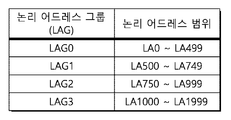
도 3a는 각각의 논리 어드레스 그룹들에 포함되는 논리 어드레스 범위를 예시적으로 설명하기 위한 도면이다.
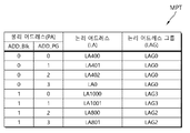
도 3b는 맵핑 테이블에 저장되는 정보를 예시적으로 설명하기 위한 도면이다.
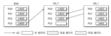
도 4는 도 2의 가비지 컬렉션 모듈에 의해서 수행되는 가비지 컬렉션 동작을 설명하기 위한 도면이다.
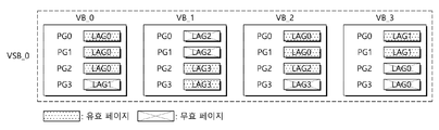
도 5는 복수의 논리 어드레스 그룹들에 대응하는 유효 데이터가 저장된 희생 블록을 예시적으로 보여주는 도면이다.
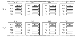
도 6은 본 발명의 실시 예에 따라, 도 5의 희생 블록에 저장된 유효 데이터가 2개의 타겟 블록들에 백업되는 경우를 설명하기 위한 도면이다.
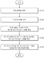
도 7은 도 6의 실시 예를 시계열적으로 설명하기 위한 순서도이다.
도 8은 본 발명의 실시 예에 따라, 도 5의 희생 블록에 저장된 유효 데이터가 1개의 타겟 블록에 백업되는 경우를 설명하기 위한 도면이다.
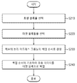
도 9는 도 8의 실시 예를 시계열적으로 설명하기 위한 순서도이다.
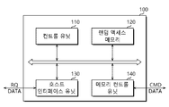
도 10은 본 발명의 실시 예에 따른 컨트롤러의 구성을 설명하기 위한 블록도이다.
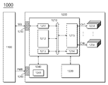
도 11은 본 발명의 실시 예에 따른 SSD를 포함하는 데이터 처리 시스템을 예시적으로 보여주는 도면이다.
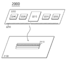
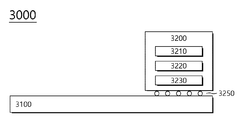
도 12는 본 발명의 실시 예에 따른 메모리 시스템을 포함하는 데이터 처리 시스템을 예시적으로 보여주는 도면이다.
도 13은 본 발명의 실시 예에 따른 메모리 시스템을 포함하는 데이터 처리 시스템을 예시적으로 보여주는 도면이다.
도 14는 본 발명의 실시 예에 따른 메모리 시스템을 포함하는 네트워크 시스템을 예시적으로 보여주는 도면이다.
도 15는 본 발명의 실시 예에 따른 메모리 시스템에 포함된 비휘발성 메모리 장치를 예시적으로 보여주는 블록도이다.
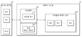
20 : 호스트 장치
100 : 컨트롤러
110 : 컨트롤 유닛
120 : 랜덤 액세스 메모리
200 : 비휘발성 메모리 장치
Claims (20)
- 각각이 기설정된 논리 어드레스 범위를 갖는 복수의 논리 어드레스 그룹들이 적용되는 메모리 시스템의 동작 방법에 있어서,
희생(victim) 블록을 선택하는 단계;
빈 블록들 중에서 복수의 타겟 블록들을 선택하는 단계;
상기 타겟 블록들 각각에 상기 논리 어드레스 그룹들 중 적어도 하나의 논리 어드레스 그룹을 맵핑하는 단계;
상기 논리 어드레스 그룹들 중에서, 상기 희생 블록에 저장된 제1 유효 데이터의 논리 어드레스를 포함하는 제1 논리 어드레스 그룹을 판단하는 단계;
상기 제1 유효 데이터를 상기 타겟 블록들 중에서 상기 제1 논리 어드레스 그룹에 맵핑된 제1 타겟 블록에 백업하는 단계를 포함하는, 방법. - 제1항에 있어서,
상기 타겟 블록들 각각에 상기 적어도 하나의 논리 어드레스 그룹을 맵핑하는 단계는,
상기 논리 어드레스 그룹들 중, 상기 희생 블록에 저장된 유효 데이터의 논리 어드레스들을 가장 많이 포함하는 논리 어드레스 그룹을 결정하는 단계;
상기 타겟 블록들 중 어느 하나의 타겟 블록에 상기 결정된 논리 어드레스 그룹을 맵핑하는 단계; 및
상기 타겟 블록들 중 다른 하나의 타겟 블록에 상기 논리 어드레스 그룹들 중 상기 결정된 논리 어드레스 그룹을 제외한 나머지 논리 어드레스 그룹들을 맵핑하는 단계를 포함하는, 방법 - 제1항에 있어서,
상기 타겟 블록들 각각에 상기 적어도 하나의 논리 어드레스 그룹을 맵핑하는 단계는,
상기 논리 어드레스 그룹들이 가지는 오프셋 값들에 따라, 상기 타겟 블록들 각각에 상기 적어도 하나의 논리 어드레스 그룹을 맵핑하는 단계를 포함하는, 방법. - 제1항에 있어서,
상기 희생 블록에 대한 맵핑 정보가 저장된 맵핑 테이블에 근거하여 상기 제1 유효 데이터를 선별하는 단계를 더 포함하는, 방법. - 제4항에 있어서,
상기 맵핑 테이블은, 상기 희생 블록에서 상기 제1 유효 데이터가 저장된 위치에 관한 물리 어드레스와 상기 제1 유효 데이터의 상기 논리 어드레스 사이의 맵핑 정보를 포함하는, 방법. - 제1항에 있어서,
상기 희생 블록 및 상기 타겟 블록들 각각은, 상기 메모리 시스템에 포함된 복수의 비휘발성 메모리 장치들에 각각 포함된 복수의 메모리 블록들을 포함하는 슈퍼 블록 단위로 설정되는, 방법. - 각각이 기설정된 논리 어드레스 범위를 갖는 복수의 논리 어드레스 그룹들이 적용되는 메모리 시스템의 동작 방법에 있어서,
희생 블록을 선택하는 단계;
빈 블록들 중에서 상기 희생 블록에 저장된 유효 데이터가 백업되는 타겟 블록을 선택하는 단계;
상기 논리 어드레스 그룹들의 백업 순서를 결정하되, 상기 백업 순서는 상기 각각의 논리 어드레스 그룹들에 대응하는 유효 데이터가 상기 타겟 블록에 백업되는 순서인, 결정하는 단계; 및
상기 백업 순서에 기초하여 상기 유효 데이터 중 선택된 유효 데이터를 상기 타겟 블록으로 백업하는 단계를 포함하는, 방법. - 제7항에 있어서,
상기 백업 순서를 결정하는 단계는,
상기 타겟 블록을 구성하는 복수의 영역들 중 유효 데이터가 가장 먼저 백업될 제1 영역을 선택하는 단계;
상기 논리 어드레스 그룹들 중 상기 제1 영역에 맵핑될 제1 논리 어드레스 그룹을 선택하는 단계를 포함하는, 방법. - 제8항에 있어서,
상기 선택된 유효 데이터를 상기 타겟 블록으로 백업하는 단계는,
상기 제1 영역에 상기 제1 논리 어드레스 그룹에 대응하는 유효 데이터를 백업하는 단계; 및
상기 복수의 영역들 중 제2 영역에 상기 논리 어드레스 그룹들 중 상기 제1 논리 어드레스 그룹 이외의 논리 어드레스 그룹들에 대응하는 유효 데이터를 백업하는 단계를 포함하는, 방법. - 제9항에 있어서,
상기 제1 영역은 제1 칩 인에이블 신호에 의하여 구동되고,
상기 제2 영역은 제2 칩 인에이블 신호에 의하여 구동되고,
상기 제1 칩 인에이블 신호는, 상기 타겟 블록을 구동하는 칩 인에이블 신호들 중 가장 먼저 생성되는 칩 인에이블 신호인, 방법. - 제8항에 있어서,
상기 제1 논리 어드레스 그룹을 선택하는 단계는,
상기 논리 어드레스 그룹들 중, 상기 희생 블록에 저장된 상기 유효 데이터에 대응하는 논리 어드레스들을 가장 많이 포함하는 논리 어드레스 그룹을 상기 제1 논리 어드레스 그룹으로 선택하는 단계를 포함하는, 방법. - 제8항에 있어서,
상기 제1 논리 어드레스 그룹을 선택하는 단계는,
상기 논리 어드레스 그룹들이 서로 다른 오프셋 값들을 가질 때, 상기 논리 어드레스 그룹들 중 기설정된 오프셋 값을 갖는 논리 어드레스 그룹을 상기 제1 논리 어드레스 그룹으로 선택하는 단계를 포함하는, 방법. - 제7항에 있어서,
상기 희생 블록에 대한 맵핑 정보가 저장된 맵핑 테이블에 근거하여 상기 유효 데이터를 선별하는 단계를 더 포함하는, 방법. - 제13항에 있어서,
상기 맵핑 테이블은, 상기 희생 블록에서 상기 유효 데이터가 저장된 위치에 관한 물리 어드레스와 상기 유효 데이터의 논리 어드레스 사이의 맵핑 정보를 포함하는, 방법. - 제7항에 있어서,
상기 희생 블록 및 상기 타겟 블록 각각은, 상기 메모리 시스템에 포함된 복수의 비휘발성 메모리 장치들에 각각 포함된 복수의 메모리 블록들을 포함하는 슈퍼 블록 단위로 설정되는, 방법. - 각각이 기설정된 논리 어드레스 범위를 갖는 복수의 논리 어드레스 그룹들이 적용되는 메모리 시스템에 있어서,
복수의 메모리 블록들을 포함하는 비휘발성 메모리 장치들; 및
상기 메모리 블록들을 상기 비휘발성 메모리 장치들에 걸쳐 복수의 슈퍼 블록들로 그룹핑하고, 상기 슈퍼 블록들 중에서 희생(victim) 블록을 선택하고, 상기 희생 블록에 대한 내부 백업 동작을 제어하도록 구성된 컨트롤러를 포함하되,
상기 컨트롤러는,
상기 논리 어드레스 그룹들 중 상기 희생 블록에 저장된 유효 데이터의 논리 어드레스들을 포함하는 논리 어드레스 그룹들을 판단하고, 상기 판단된 논리 어드레스 그룹들에 맵핑된 위치들에 상기 유효 데이터를 백업하는, 메모리 시스템. - 제16항에 있어서,
상기 컨트롤러는,
빈 슈퍼 블록들 중에서 복수의 타겟 블록들을 선택하고,
상기 타겟 블록들 각각에 상기 논리 어드레스 그룹들 중 적어도 하나의 논리 어드레스 그룹을 맵핑하고,
상기 논리 어드레스 그룹들 중에서, 상기 희생 블록에 저장된 제1 유효 데이터의 논리 어드레스를 포함하는 제1 논리 어드레스 그룹을 판단하고,
상기 제1 유효 데이터를 상기 타겟 블록들 중에서 상기 제1 논리 어드레스 그룹에 맵핑된 제1 타겟 블록에 백업하는, 메모리 시스템. - 제17항에 있어서,
상기 컨트롤러는,
상기 논리 어드레스 그룹들 중, 상기 희생 블록에 저장된 유효 데이터의 논리 어드레스들을 가장 많이 포함하는 논리 어드레스 그룹을 결정하고,
상기 타겟 블록들 중 어느 하나의 타겟 블록에 상기 결정된 논리 어드레스 그룹을 맵핑하고,
상기 타겟 블록들 중 다른 하나의 타겟 블록에 상기 논리 어드레스 그룹들 중 상기 결정된 논리 어드레스 그룹을 제외한 나머지 논리 어드레스 그룹들을 맵핑하는, 메모리 시스템. - 제16항에 있어서,
상기 컨트롤러는,
빈 슈퍼 블록들 중에서 타겟 블록을 선택하고,
상기 타겟 블록에 포함된 복수의 영역들 각각에 상기 논리 어드레스 그룹들 중 적어도 하나의 논리 어드레스 그룹을 맵핑하되, 상기 영역들은 서로 다른 칩 인에이블 신호들에 의하여 각각 구동되고,
상기 논리 어드레스 그룹들 중에서, 상기 희생 블록에 저장된 제1 유효 데이터의 논리 어드레스를 포함하는 제1 논리 어드레스 그룹을 판단하고,
상기 제1 유효 데이터를 상기 영역들 중에서 상기 제1 논리 어드레스 그룹에 맵핑된 제1 영역에 백업하는, 메모리 시스템. - 제19항에 있어서,
상기 컨트롤러는,
상기 제1 영역에 상기 제1 논리 어드레스 그룹을 맵핑하고, 상기 영역들 중 제2 영역에 상기 제1 논리 어드레스 그룹을 제외한 나머지 논리 어드레스 그룹들을 맵핑하고,
상기 제1 논리 어드레스 그룹은,
상기 논리 어드레스 그룹들 중, 상기 희생 블록에 저장된 유효 데이터의 논리 어드레스들을 가장 많이 포함하는 논리 어드레스 그룹이고,
상기 제1 영역은,
상기 칩 인에이블 신호들 중 가장 먼저 생성되는 칩 인에이블 신호에 의해 구동되는, 메모리 시스템.
Priority Applications (3)
| Application Number | Priority Date | Filing Date | Title |
|---|---|---|---|
| KR1020180111661A KR102585883B1 (ko) | 2018-09-18 | 2018-09-18 | 메모리 시스템의 동작 방법 및 메모리 시스템 |
| US16/224,955 US11086772B2 (en) | 2018-09-18 | 2018-12-19 | Memory system performing garbage collection operation and operating method of memory system |
| CN201811636994.0A CN110908594B (zh) | 2018-09-18 | 2018-12-29 | 存储器系统的操作方法和存储器系统 |
Applications Claiming Priority (1)
| Application Number | Priority Date | Filing Date | Title |
|---|---|---|---|
| KR1020180111661A KR102585883B1 (ko) | 2018-09-18 | 2018-09-18 | 메모리 시스템의 동작 방법 및 메모리 시스템 |
Publications (2)
| Publication Number | Publication Date |
|---|---|
| KR20200032527A true KR20200032527A (ko) | 2020-03-26 |
| KR102585883B1 KR102585883B1 (ko) | 2023-10-10 |
Family
ID=69774065
Family Applications (1)
| Application Number | Title | Priority Date | Filing Date |
|---|---|---|---|
| KR1020180111661A Active KR102585883B1 (ko) | 2018-09-18 | 2018-09-18 | 메모리 시스템의 동작 방법 및 메모리 시스템 |
Country Status (3)
| Country | Link |
|---|---|
| US (1) | US11086772B2 (ko) |
| KR (1) | KR102585883B1 (ko) |
| CN (1) | CN110908594B (ko) |
Families Citing this family (7)
| Publication number | Priority date | Publication date | Assignee | Title |
|---|---|---|---|---|
| TWI718492B (zh) * | 2019-03-12 | 2021-02-11 | 群聯電子股份有限公司 | 資料儲存方法、記憶體儲存裝置及記憶體控制電路單元 |
| KR102796097B1 (ko) * | 2019-03-18 | 2025-04-16 | 에스케이하이닉스 주식회사 | 데이터 저장 장치 및 이를 포함하는 컴퓨팅 장치와 그 동작 방법 |
| KR102869315B1 (ko) * | 2019-07-24 | 2025-10-14 | 에스케이하이닉스 주식회사 | 메모리 시스템 및 메모리 시스템의 동작 방법 |
| KR102809393B1 (ko) * | 2020-08-28 | 2025-05-21 | 에스케이하이닉스 주식회사 | 저장 장치 및 그 동작 방법 |
| US20220222008A1 (en) * | 2021-01-14 | 2022-07-14 | Silicon Motion, Inc. | Method for managing flash memory module and associated flash memory controller and memory device |
| TWI766582B (zh) * | 2021-02-17 | 2022-06-01 | 群聯電子股份有限公司 | 有效資料合併方法、記憶體儲存裝置及記憶體控制電路單元 |
| CN115495287B (zh) * | 2022-11-16 | 2024-04-09 | 珠海妙存科技有限公司 | 一种mlc nand的备份数据方法、装置及电子设备 |
Citations (4)
| Publication number | Priority date | Publication date | Assignee | Title |
|---|---|---|---|---|
| KR20100078450A (ko) * | 2008-12-30 | 2010-07-08 | 아주대학교산학협력단 | 플래시 메모리 장치 및 플래시 메모리 장치에서의 메모리 관리 방법 |
| JP2015001908A (ja) * | 2013-06-17 | 2015-01-05 | 富士通株式会社 | 情報処理装置、制御回路、制御プログラム、および制御方法 |
| US20170286286A1 (en) * | 2016-03-29 | 2017-10-05 | Micron Technology, Inc. | Memory devices including dynamic superblocks, and related methods and electronic systems |
| KR20180064542A (ko) * | 2015-10-30 | 2018-06-14 | 마이크론 테크놀로지, 인크. | 공유 버스 상에서의 다수의 디바이스들을 위한 데이터 전달 기술들 |
Family Cites Families (12)
| Publication number | Priority date | Publication date | Assignee | Title |
|---|---|---|---|---|
| JP4633802B2 (ja) * | 2005-12-09 | 2011-02-16 | パナソニック株式会社 | 不揮発性記憶装置及びデータ読み出し方法及び管理テーブル作成方法 |
| CN101169762A (zh) * | 2006-10-27 | 2008-04-30 | 北京中电华大电子设计有限责任公司 | 一种面向智能卡的软硬件协同保护机制 |
| US8166233B2 (en) * | 2009-07-24 | 2012-04-24 | Lsi Corporation | Garbage collection for solid state disks |
| US8463826B2 (en) * | 2009-09-03 | 2013-06-11 | Apple Inc. | Incremental garbage collection for non-volatile memories |
| CN102081576B (zh) * | 2011-03-01 | 2012-07-11 | 华中科技大学 | 一种闪存的磨损平衡方法 |
| CN103150261B (zh) * | 2013-03-11 | 2017-02-08 | 北京忆恒创源科技有限公司 | 用于同时访问多个固态盘的方法与装置 |
| US9753653B2 (en) * | 2015-04-14 | 2017-09-05 | Sandisk Technologies Llc | High-priority NAND operations management |
| KR102509540B1 (ko) | 2015-06-30 | 2023-03-14 | 삼성전자주식회사 | 저장 장치 및 그것의 가비지 컬렉션 방법 |
| CN106445740A (zh) * | 2016-09-22 | 2017-02-22 | 深圳市先天海量信息技术有限公司 | 固态硬盘中nand闪存数据的控制方法及控制系统 |
| JP2018181213A (ja) * | 2017-04-20 | 2018-11-15 | 富士通株式会社 | ストレージ制御装置、ストレージ制御方法及びストレージ制御プログラム |
| JP2018181207A (ja) * | 2017-04-20 | 2018-11-15 | 富士通株式会社 | ストレージ制御装置、ストレージ制御方法及びストレージ制御プログラム |
| US10452536B2 (en) * | 2017-06-12 | 2019-10-22 | Western Digital Technologies, Inc. | Dynamic management of garbage collection and overprovisioning for host stream storage |
-
2018
- 2018-09-18 KR KR1020180111661A patent/KR102585883B1/ko active Active
- 2018-12-19 US US16/224,955 patent/US11086772B2/en active Active
- 2018-12-29 CN CN201811636994.0A patent/CN110908594B/zh active Active
Patent Citations (4)
| Publication number | Priority date | Publication date | Assignee | Title |
|---|---|---|---|---|
| KR20100078450A (ko) * | 2008-12-30 | 2010-07-08 | 아주대학교산학협력단 | 플래시 메모리 장치 및 플래시 메모리 장치에서의 메모리 관리 방법 |
| JP2015001908A (ja) * | 2013-06-17 | 2015-01-05 | 富士通株式会社 | 情報処理装置、制御回路、制御プログラム、および制御方法 |
| KR20180064542A (ko) * | 2015-10-30 | 2018-06-14 | 마이크론 테크놀로지, 인크. | 공유 버스 상에서의 다수의 디바이스들을 위한 데이터 전달 기술들 |
| US20170286286A1 (en) * | 2016-03-29 | 2017-10-05 | Micron Technology, Inc. | Memory devices including dynamic superblocks, and related methods and electronic systems |
Also Published As
| Publication number | Publication date |
|---|---|
| CN110908594A (zh) | 2020-03-24 |
| US20200089603A1 (en) | 2020-03-19 |
| CN110908594B (zh) | 2023-08-25 |
| US11086772B2 (en) | 2021-08-10 |
| KR102585883B1 (ko) | 2023-10-10 |
Similar Documents
| Publication | Publication Date | Title |
|---|---|---|
| US10802733B2 (en) | Methods and apparatus for configuring storage tiers within SSDs | |
| US9208079B2 (en) | Solid state memory (SSM), computer system including an SSM, and method of operating an SSM | |
| KR102585883B1 (ko) | 메모리 시스템의 동작 방법 및 메모리 시스템 | |
| CN107168886B (zh) | 数据存储装置及其操作方法 | |
| KR102233400B1 (ko) | 데이터 저장 장치 및 그것의 동작 방법 | |
| KR102544162B1 (ko) | 데이터 저장 장치 및 그것의 동작 방법 | |
| US20190317892A1 (en) | Memory system, data processing system, and operating method of memory system | |
| KR102835407B1 (ko) | 데이터 저장 장치 및 그것의 동작 방법 | |
| KR20210144249A (ko) | 저장 장치 및 이의 동작 방법 | |
| KR102811643B1 (ko) | 데이터 저장 장치 및 그것의 동작 방법 | |
| US11169871B2 (en) | Data storage device and operating method thereof | |
| KR102746969B1 (ko) | 데이터 저장 장치 및 그것의 동작 방법 | |
| KR102703487B1 (ko) | 데이터 저장 장치 및 그것의 동작 방법 | |
| US20190278703A1 (en) | Memory system, operating method thereof and electronic device | |
| US20220229775A1 (en) | Data storage device and operating method thereof | |
| CN108804338B (zh) | 数据存储装置及其操作方法 | |
| US20230126685A1 (en) | Storage device and electronic system | |
| KR102873594B1 (ko) | 데이터 저장 장치 및 그것의 동작 방법 | |
| KR20210079894A (ko) | 데이터 저장 장치 및 그것의 동작 방법 | |
| US20220164119A1 (en) | Controller, and memory system and data processing system including the same |
Legal Events
| Date | Code | Title | Description |
|---|---|---|---|
| PA0109 | Patent application |
St.27 status event code: A-0-1-A10-A12-nap-PA0109 |
|
| PG1501 | Laying open of application |
St.27 status event code: A-1-1-Q10-Q12-nap-PG1501 |
|
| PA0201 | Request for examination |
St.27 status event code: A-1-2-D10-D11-exm-PA0201 |
|
| D13-X000 | Search requested |
St.27 status event code: A-1-2-D10-D13-srh-X000 |
|
| D14-X000 | Search report completed |
St.27 status event code: A-1-2-D10-D14-srh-X000 |
|
| E902 | Notification of reason for refusal | ||
| PE0902 | Notice of grounds for rejection |
St.27 status event code: A-1-2-D10-D21-exm-PE0902 |
|
| E13-X000 | Pre-grant limitation requested |
St.27 status event code: A-2-3-E10-E13-lim-X000 |
|
| P11-X000 | Amendment of application requested |
St.27 status event code: A-2-2-P10-P11-nap-X000 |
|
| P13-X000 | Application amended |
St.27 status event code: A-2-2-P10-P13-nap-X000 |
|
| E701 | Decision to grant or registration of patent right | ||
| PE0701 | Decision of registration |
St.27 status event code: A-1-2-D10-D22-exm-PE0701 |
|
| PR0701 | Registration of establishment |
St.27 status event code: A-2-4-F10-F11-exm-PR0701 |
|
| PR1002 | Payment of registration fee |
St.27 status event code: A-2-2-U10-U11-oth-PR1002 Fee payment year number: 1 |
|
| PG1601 | Publication of registration |
St.27 status event code: A-4-4-Q10-Q13-nap-PG1601 |