KR20200034930A - 자기 디바이스 및 자기 랜덤 액세스 메모리 - Google Patents
자기 디바이스 및 자기 랜덤 액세스 메모리 Download PDFInfo
- Publication number
- KR20200034930A KR20200034930A KR1020190108875A KR20190108875A KR20200034930A KR 20200034930 A KR20200034930 A KR 20200034930A KR 1020190108875 A KR1020190108875 A KR 1020190108875A KR 20190108875 A KR20190108875 A KR 20190108875A KR 20200034930 A KR20200034930 A KR 20200034930A
- Authority
- KR
- South Korea
- Prior art keywords
- layer
- magnetic
- diffusion barrier
- magnetic layer
- barrier layer
- Prior art date
- Legal status (The legal status is an assumption and is not a legal conclusion. Google has not performed a legal analysis and makes no representation as to the accuracy of the status listed.)
- Granted
Links
Images





Classifications
-
- H—ELECTRICITY
- H10—SEMICONDUCTOR DEVICES; ELECTRIC SOLID-STATE DEVICES NOT OTHERWISE PROVIDED FOR
- H10N—ELECTRIC SOLID-STATE DEVICES NOT OTHERWISE PROVIDED FOR
- H10N50/00—Galvanomagnetic devices
- H10N50/10—Magnetoresistive devices
-
- H—ELECTRICITY
- H10—SEMICONDUCTOR DEVICES; ELECTRIC SOLID-STATE DEVICES NOT OTHERWISE PROVIDED FOR
- H10N—ELECTRIC SOLID-STATE DEVICES NOT OTHERWISE PROVIDED FOR
- H10N50/00—Galvanomagnetic devices
- H10N50/20—Spin-polarised current-controlled devices
-
- H01L43/08—
-
- G—PHYSICS
- G11—INFORMATION STORAGE
- G11C—STATIC STORES
- G11C11/00—Digital stores characterised by the use of particular electric or magnetic storage elements; Storage elements therefor
- G11C11/02—Digital stores characterised by the use of particular electric or magnetic storage elements; Storage elements therefor using magnetic elements
- G11C11/16—Digital stores characterised by the use of particular electric or magnetic storage elements; Storage elements therefor using magnetic elements using elements in which the storage effect is based on magnetic spin effect
- G11C11/161—Digital stores characterised by the use of particular electric or magnetic storage elements; Storage elements therefor using magnetic elements using elements in which the storage effect is based on magnetic spin effect details concerning the memory cell structure, e.g. the layers of the ferromagnetic memory cell
-
- G—PHYSICS
- G11—INFORMATION STORAGE
- G11C—STATIC STORES
- G11C11/00—Digital stores characterised by the use of particular electric or magnetic storage elements; Storage elements therefor
- G11C11/02—Digital stores characterised by the use of particular electric or magnetic storage elements; Storage elements therefor using magnetic elements
- G11C11/16—Digital stores characterised by the use of particular electric or magnetic storage elements; Storage elements therefor using magnetic elements using elements in which the storage effect is based on magnetic spin effect
- G11C11/165—Auxiliary circuits
- G11C11/1675—Writing or programming circuits or methods
-
- H01L43/02—
-
- H01L43/10—
-
- H01L43/12—
-
- H—ELECTRICITY
- H10—SEMICONDUCTOR DEVICES; ELECTRIC SOLID-STATE DEVICES NOT OTHERWISE PROVIDED FOR
- H10B—ELECTRONIC MEMORY DEVICES
- H10B61/00—Magnetic memory devices, e.g. magnetoresistive RAM [MRAM] devices
-
- H—ELECTRICITY
- H10—SEMICONDUCTOR DEVICES; ELECTRIC SOLID-STATE DEVICES NOT OTHERWISE PROVIDED FOR
- H10B—ELECTRONIC MEMORY DEVICES
- H10B61/00—Magnetic memory devices, e.g. magnetoresistive RAM [MRAM] devices
- H10B61/10—Magnetic memory devices, e.g. magnetoresistive RAM [MRAM] devices comprising components having two electrodes, e.g. diodes or MIM elements
-
- H—ELECTRICITY
- H10—SEMICONDUCTOR DEVICES; ELECTRIC SOLID-STATE DEVICES NOT OTHERWISE PROVIDED FOR
- H10B—ELECTRONIC MEMORY DEVICES
- H10B61/00—Magnetic memory devices, e.g. magnetoresistive RAM [MRAM] devices
- H10B61/20—Magnetic memory devices, e.g. magnetoresistive RAM [MRAM] devices comprising components having three or more electrodes, e.g. transistors
- H10B61/22—Magnetic memory devices, e.g. magnetoresistive RAM [MRAM] devices comprising components having three or more electrodes, e.g. transistors of the field-effect transistor [FET] type
-
- H—ELECTRICITY
- H10—SEMICONDUCTOR DEVICES; ELECTRIC SOLID-STATE DEVICES NOT OTHERWISE PROVIDED FOR
- H10N—ELECTRIC SOLID-STATE DEVICES NOT OTHERWISE PROVIDED FOR
- H10N50/00—Galvanomagnetic devices
- H10N50/01—Manufacture or treatment
-
- H—ELECTRICITY
- H10—SEMICONDUCTOR DEVICES; ELECTRIC SOLID-STATE DEVICES NOT OTHERWISE PROVIDED FOR
- H10N—ELECTRIC SOLID-STATE DEVICES NOT OTHERWISE PROVIDED FOR
- H10N50/00—Galvanomagnetic devices
- H10N50/80—Constructional details
-
- H—ELECTRICITY
- H10—SEMICONDUCTOR DEVICES; ELECTRIC SOLID-STATE DEVICES NOT OTHERWISE PROVIDED FOR
- H10N—ELECTRIC SOLID-STATE DEVICES NOT OTHERWISE PROVIDED FOR
- H10N50/00—Galvanomagnetic devices
- H10N50/80—Constructional details
- H10N50/85—Materials of the active region
Landscapes
- Engineering & Computer Science (AREA)
- Computer Hardware Design (AREA)
- Manufacturing & Machinery (AREA)
- Hall/Mr Elements (AREA)
- Mram Or Spin Memory Techniques (AREA)
Abstract
Description
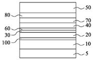
도 1b는 본 개시의 한 실시예에 따른 SOT MRAM 셀의 개략도이다.
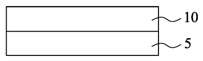
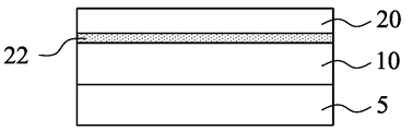
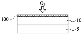
도 2a, 도 2b, 도 2c, 및 도 2d는 본 개시의 실시예에 따른 SOT MRAM 셀의 제조 동작의 개략적 단면도를 도시한다.
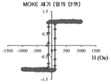
도 3a, 도 3b, 도 3c, 및 도 3d는, 확산 배리어층이 있는 SOT 자기 디바이스 및 확산 배리어층이 없는 SOT 자기 디바이스의 수직 자기 이방성의 실험 결과를 도시한다.
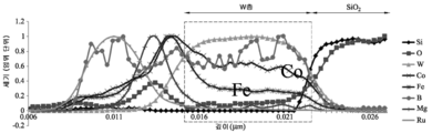
도 4a 및 도 4b는 2차 이온 질량 분광측정의 실험 결과를 도시한다.
Claims (10)
- 스핀-궤도-토크(SOT, spin-orbit-torque) 자기 디바이스에 있어서,
하단 금속층;
상기 하단 금속층 위에 배치된 제1 자기층;
상기 제1 자기층 위에 배치된 스페이서층;
상기 스페이서층 위에 배치된 제2 자기층; 및
상기 하단 금속층과 상기 제1 자기층 사이에 배치된 확산 배리어층
을 포함하며,
상기 확산 배리어층은 상기 제1 자기층의 금속 원소가 상기 하단 금속층 내부로 확산되는 것을 억제하는, SOT 자기 디바이스. - 제1항에 있어서, 상기 제1 자기층은 철 및 코발트를 포함하는, SOT 자기 디바이스.
- 제2항에 있어서,
상기 확산 배리어층은 철을 포함하고,
상기 확산 배리어층 내의 철의 원자 백분율은 상기 제1 자기층 내의 철의 원자 백분율보다 더 높은, SOT 자기 디바이스. - 제3항에 있어서, 상기 제1 자기층 및 상기 확산 배리어층은 붕소를 더 포함하는, SOT 자기 디바이스.
- 제2항에 있어서,
상기 확산 배리어층은 코발트를 포함하고,
상기 확산 배리어층 내의 코발트의 원자 백분율은 상기 제1 자기층 내의 코발트의 원자 백분율보다 더 높은, SOT 자기 디바이스. - 제1항에 있어서, 상기 스페이서층과 상기 제2 자기층 사이에 배치된 중간 금속층을 더 포함하는, SOT 자기 디바이스.
- 제1항에 있어서, 상기 제2 자기층 위에 배치된 상단 금속층을 더 포함하는, SOT 자기 디바이스.
- 제1항에 있어서, 상기 제2 자기층은 철, 코발트, 및 붕소를 포함하는, SOT 자기 디바이스.
- 스핀-궤도-토크(SOT) 자기 디바이스에 있어서,
하단 금속층;
상기 하단 금속층 위에 배치된 제1 자기층;
상기 제1 자기층 위에 배치된 스페이서층;
상기 스페이서층 위에 배치된 제2 자기층; 및
자기 불활성층과 상기 제1 자기층 사이에 배치된 확산 배리어층
을 포함하며,
상기 자기 불활성층은 상기 하단 금속층과 상기 제1 자기층 사이에 배치되어 형성되고,
상기 확산 배리어층은 상기 제1 자기층의 금속 원소가 상기 하단 금속층 내부로 확산되는 것을 억제하는, SOT 자기 디바이스. - 스핀-궤도-토크(SOT) 자기 디바이스를 제조하는 방법에 있어서,
하단 금속층 위에 제1 자기층을 형성하는 단계;
상기 하단 금속층과 상기 제1 자기층 사이에 확산 배리어층이 형성되도록, 상기 제1 자기층을 처리하는 단계;
상기 제1 자기층 위에 스페이서층을 형성하는 단계;
상기 스페이서층 위에 중간 금속층을 형성하는 단계; 및
상기 중간 금속층 위에 제2 자기층을 형성하는 단계
를 포함하며,
상기 확산 배리어층은, 450°C를 초과하는 후속 열 공정에서 상기 제1 자기층의 금속 원소가 상기 하단 금속층 내부로 확산되는 것을 억제하는, SOT 자기 디바이스를 제조하는 방법.
Applications Claiming Priority (4)
| Application Number | Priority Date | Filing Date | Title |
|---|---|---|---|
| US201862734484P | 2018-09-21 | 2018-09-21 | |
| US62/734,484 | 2018-09-21 | ||
| US16/427,308 | 2019-05-30 | ||
| US16/427,308 US10879307B2 (en) | 2018-09-21 | 2019-05-30 | Magnetic device and magnetic random access memory |
Publications (2)
| Publication Number | Publication Date |
|---|---|
| KR20200034930A true KR20200034930A (ko) | 2020-04-01 |
| KR102287559B1 KR102287559B1 (ko) | 2021-08-11 |
Family
ID=69725086
Family Applications (1)
| Application Number | Title | Priority Date | Filing Date |
|---|---|---|---|
| KR1020190108875A Active KR102287559B1 (ko) | 2018-09-21 | 2019-09-03 | 자기 디바이스 및 자기 랜덤 액세스 메모리 |
Country Status (5)
| Country | Link |
|---|---|
| US (3) | US10879307B2 (ko) |
| KR (1) | KR102287559B1 (ko) |
| CN (2) | CN120957591A (ko) |
| DE (1) | DE102019115922B4 (ko) |
| TW (1) | TWI738051B (ko) |
Cited By (3)
| Publication number | Priority date | Publication date | Assignee | Title |
|---|---|---|---|---|
| KR20220098692A (ko) * | 2021-01-04 | 2022-07-12 | 타이완 세미콘덕터 매뉴팩쳐링 컴퍼니 리미티드 | 메모리 디바이스 및 그 제조 방법 |
| KR20230040533A (ko) * | 2021-09-16 | 2023-03-23 | 삼성전자주식회사 | 자기 저항 메모리 소자 |
| WO2024123561A3 (en) * | 2022-12-05 | 2025-09-12 | Micron Technology, Inc. | Memory cell protective layers in a three-dimensional memory array |
Families Citing this family (6)
| Publication number | Priority date | Publication date | Assignee | Title |
|---|---|---|---|---|
| US10879307B2 (en) * | 2018-09-21 | 2020-12-29 | Taiwan Semiconductor Manufacturing Co., Ltd. | Magnetic device and magnetic random access memory |
| US11348715B2 (en) * | 2019-06-10 | 2022-05-31 | Samsung Electronics Co., Ltd. | Semiconductor device and method of making the same |
| CN111682105B (zh) * | 2020-06-23 | 2023-04-07 | 浙江驰拓科技有限公司 | 一种磁存储器件及其写入方法、逻辑器件 |
| CN113451503B (zh) * | 2020-12-31 | 2023-03-17 | 北京航空航天大学 | 多功能磁性随机存储单元、存储器及设备 |
| US11706999B2 (en) * | 2021-01-13 | 2023-07-18 | Taiwan Semiconductor Manufacturing Co., Ltd. | Semiconductor device and manufacturing method of semiconductor device |
| CN119156121B (zh) * | 2024-11-11 | 2025-04-18 | 青岛海存微电子有限公司 | 半导体器件及其制备方法 |
Citations (4)
| Publication number | Priority date | Publication date | Assignee | Title |
|---|---|---|---|---|
| US6347049B1 (en) * | 2001-07-25 | 2002-02-12 | International Business Machines Corporation | Low resistance magnetic tunnel junction device with bilayer or multilayer tunnel barrier |
| KR20170057464A (ko) * | 2014-10-16 | 2017-05-24 | 마이크론 테크놀로지, 인크 | 메모리 셀들, 반도체 디바이스들, 및 제조 방법들 |
| KR20170093546A (ko) * | 2016-02-05 | 2017-08-16 | 한양대학교 산학협력단 | 메모리 소자 |
| KR20170105395A (ko) * | 2016-03-09 | 2017-09-19 | 삼성전자주식회사 | 스핀 전달 토크 응용에 사용 가능하고 자기 배리어층을 포함하는 자기 접합을 제공하기 위한 방법 및 시스템 |
Family Cites Families (17)
| Publication number | Priority date | Publication date | Assignee | Title |
|---|---|---|---|---|
| KR100626390B1 (ko) * | 2005-02-07 | 2006-09-20 | 삼성전자주식회사 | 자기 메모리 소자 및 그 형성 방법 |
| JP2006319259A (ja) * | 2005-05-16 | 2006-11-24 | Fujitsu Ltd | 強磁性トンネル接合素子、これを用いた磁気ヘッド、磁気記録装置、および磁気メモリ装置 |
| JP4877575B2 (ja) * | 2005-05-19 | 2012-02-15 | 日本電気株式会社 | 磁気ランダムアクセスメモリ |
| KR100773544B1 (ko) * | 2006-02-09 | 2007-11-05 | 삼성전자주식회사 | 확산 방지층을 포함하는 자기 저항 소자 |
| US7532505B1 (en) | 2006-07-17 | 2009-05-12 | Grandis, Inc. | Method and system for using a pulsed field to assist spin transfer induced switching of magnetic memory elements |
| US7508042B2 (en) | 2006-12-22 | 2009-03-24 | Magic Technologies, Inc. | Spin transfer MRAM device with magnetic biasing |
| US20100148167A1 (en) * | 2008-12-12 | 2010-06-17 | Everspin Technologies, Inc. | Magnetic tunnel junction stack |
| JP2013048210A (ja) | 2011-07-22 | 2013-03-07 | Toshiba Corp | 磁気抵抗素子 |
| JP2013197409A (ja) * | 2012-03-21 | 2013-09-30 | Toshiba Corp | 磁気抵抗素子及びそれを備える磁気ランダムアクセスメモリ |
| US9076537B2 (en) | 2012-08-26 | 2015-07-07 | Samsung Electronics Co., Ltd. | Method and system for providing a magnetic tunneling junction using spin-orbit interaction based switching and memories utilizing the magnetic tunneling junction |
| WO2016209267A1 (en) | 2015-06-26 | 2016-12-29 | Intel Corporation | Low stray field magnetic memory |
| JP6200471B2 (ja) | 2015-09-14 | 2017-09-20 | 株式会社東芝 | 磁気メモリ |
| CN109155360A (zh) | 2016-02-05 | 2019-01-04 | 汉阳大学校产学协力团 | 存储器件 |
| TWI581261B (zh) | 2016-03-15 | 2017-05-01 | 賴志煌 | 自旋軌道扭力式磁性隨存記憶體及其寫入方法 |
| US10546997B2 (en) * | 2016-12-02 | 2020-01-28 | Regents Of The University Of Minnesota | Magnetic structures including FePd |
| US11508903B2 (en) * | 2018-06-28 | 2022-11-22 | Intel Corporation | Spin orbit torque device with insertion layer between spin orbit torque electrode and free layer for improved performance |
| US10879307B2 (en) * | 2018-09-21 | 2020-12-29 | Taiwan Semiconductor Manufacturing Co., Ltd. | Magnetic device and magnetic random access memory |
-
2019
- 2019-05-30 US US16/427,308 patent/US10879307B2/en active Active
- 2019-06-12 DE DE102019115922.9A patent/DE102019115922B4/de active Active
- 2019-09-03 KR KR1020190108875A patent/KR102287559B1/ko active Active
- 2019-09-04 TW TW108131940A patent/TWI738051B/zh active
- 2019-09-20 CN CN202510871281.6A patent/CN120957591A/zh active Pending
- 2019-09-20 CN CN201910891688.XA patent/CN110943157A/zh active Pending
-
2020
- 2020-12-28 US US17/135,805 patent/US11437434B2/en active Active
-
2022
- 2022-07-27 US US17/875,133 patent/US11963366B2/en active Active
Patent Citations (4)
| Publication number | Priority date | Publication date | Assignee | Title |
|---|---|---|---|---|
| US6347049B1 (en) * | 2001-07-25 | 2002-02-12 | International Business Machines Corporation | Low resistance magnetic tunnel junction device with bilayer or multilayer tunnel barrier |
| KR20170057464A (ko) * | 2014-10-16 | 2017-05-24 | 마이크론 테크놀로지, 인크 | 메모리 셀들, 반도체 디바이스들, 및 제조 방법들 |
| KR20170093546A (ko) * | 2016-02-05 | 2017-08-16 | 한양대학교 산학협력단 | 메모리 소자 |
| KR20170105395A (ko) * | 2016-03-09 | 2017-09-19 | 삼성전자주식회사 | 스핀 전달 토크 응용에 사용 가능하고 자기 배리어층을 포함하는 자기 접합을 제공하기 위한 방법 및 시스템 |
Cited By (4)
| Publication number | Priority date | Publication date | Assignee | Title |
|---|---|---|---|---|
| KR20220098692A (ko) * | 2021-01-04 | 2022-07-12 | 타이완 세미콘덕터 매뉴팩쳐링 컴퍼니 리미티드 | 메모리 디바이스 및 그 제조 방법 |
| US12156479B2 (en) | 2021-01-04 | 2024-11-26 | Taiwan Semiconductor Manufacturing Co., Ltd. | Memory device and manufacturing method thereof |
| KR20230040533A (ko) * | 2021-09-16 | 2023-03-23 | 삼성전자주식회사 | 자기 저항 메모리 소자 |
| WO2024123561A3 (en) * | 2022-12-05 | 2025-09-12 | Micron Technology, Inc. | Memory cell protective layers in a three-dimensional memory array |
Also Published As
| Publication number | Publication date |
|---|---|
| TWI738051B (zh) | 2021-09-01 |
| KR102287559B1 (ko) | 2021-08-11 |
| US11437434B2 (en) | 2022-09-06 |
| TW202029542A (zh) | 2020-08-01 |
| DE102019115922B4 (de) | 2022-05-25 |
| US20220375993A1 (en) | 2022-11-24 |
| CN110943157A (zh) | 2020-03-31 |
| CN120957591A (zh) | 2025-11-14 |
| US20210118952A1 (en) | 2021-04-22 |
| US10879307B2 (en) | 2020-12-29 |
| US11963366B2 (en) | 2024-04-16 |
| US20200098407A1 (en) | 2020-03-26 |
| DE102019115922A1 (de) | 2020-03-26 |
Similar Documents
| Publication | Publication Date | Title |
|---|---|---|
| KR102287559B1 (ko) | 자기 디바이스 및 자기 랜덤 액세스 메모리 | |
| US10249817B2 (en) | Magnetic device | |
| US8081505B2 (en) | Magnetoresistive element and method of manufacturing the same | |
| KR102397904B1 (ko) | 낮은 보론 농도를 갖는 영역 및 높은 보론 농도를 갖는 영역을 포함하는 자유 층, 자기 저항 셀, 및 자기 저항 메모리 소자, 및 그 제조 방법 | |
| KR102335104B1 (ko) | 자기 소자 | |
| US10431733B2 (en) | Perpendicular magnetic tunnel junction devices with high thermal stability | |
| KR102398190B1 (ko) | 자기 디바이스 및 자기 랜덤 액세스 메모리 | |
| US11342496B2 (en) | Semiconductor memory structure with magnetic tunneling junction stack and method for forming the same | |
| US9735347B2 (en) | Magnetic memory device and method of manufacturing the same | |
| US8836000B1 (en) | Bottom-type perpendicular magnetic tunnel junction (pMTJ) element with thermally stable amorphous blocking layers | |
| US20130249025A1 (en) | Magnetoresistive element and magnetoresistive random access memory with the same | |
| US8710604B2 (en) | Magnetoresistive element and manufacturing method of the same | |
| US20200052191A1 (en) | Magnetic tunnel junction element with a robust reference layer | |
| US20170338402A1 (en) | Noble metal cap layer for a metal oxide cap of a magnetic tunnel junction structure | |
| US11763972B2 (en) | Magnetic tunnel junction element with a robust reference layer | |
| US11935677B2 (en) | Magnetic device | |
| US20170338404A1 (en) | Fabricating a cap layer for a magnetic random access memory (mram) device | |
| CN113328033B (zh) | 半导体结构及其形成方法 | |
| US12310254B2 (en) | Magnetic device | |
| US20240164219A1 (en) | Fast switching mram having an aluminum-manganese-germanium free layer combined with a chromium diffusion barrier |
Legal Events
| Date | Code | Title | Description |
|---|---|---|---|
| PA0109 | Patent application |
St.27 status event code: A-0-1-A10-A12-nap-PA0109 |
|
| PA0201 | Request for examination |
St.27 status event code: A-1-2-D10-D11-exm-PA0201 |
|
| R18-X000 | Changes to party contact information recorded |
St.27 status event code: A-3-3-R10-R18-oth-X000 |
|
| PG1501 | Laying open of application |
St.27 status event code: A-1-1-Q10-Q12-nap-PG1501 |
|
| E902 | Notification of reason for refusal | ||
| PE0902 | Notice of grounds for rejection |
St.27 status event code: A-1-2-D10-D21-exm-PE0902 |
|
| T11-X000 | Administrative time limit extension requested |
St.27 status event code: U-3-3-T10-T11-oth-X000 |
|
| T11-X000 | Administrative time limit extension requested |
St.27 status event code: U-3-3-T10-T11-oth-X000 |
|
| P11-X000 | Amendment of application requested |
St.27 status event code: A-2-2-P10-P11-nap-X000 |
|
| P13-X000 | Application amended |
St.27 status event code: A-2-2-P10-P13-nap-X000 |
|
| E701 | Decision to grant or registration of patent right | ||
| PE0701 | Decision of registration |
St.27 status event code: A-1-2-D10-D22-exm-PE0701 |
|
| GRNT | Written decision to grant | ||
| PR0701 | Registration of establishment |
St.27 status event code: A-2-4-F10-F11-exm-PR0701 |
|
| PR1002 | Payment of registration fee |
St.27 status event code: A-2-2-U10-U11-oth-PR1002 Fee payment year number: 1 |
|
| PG1601 | Publication of registration |
St.27 status event code: A-4-4-Q10-Q13-nap-PG1601 |
|
| P22-X000 | Classification modified |
St.27 status event code: A-4-4-P10-P22-nap-X000 |
|
| P22-X000 | Classification modified |
St.27 status event code: A-4-4-P10-P22-nap-X000 |
|
| PR1001 | Payment of annual fee |
St.27 status event code: A-4-4-U10-U11-oth-PR1001 Fee payment year number: 4 |
|
| P22-X000 | Classification modified |
St.27 status event code: A-4-4-P10-P22-nap-X000 |
|
| PR1001 | Payment of annual fee |
St.27 status event code: A-4-4-U10-U11-oth-PR1001 Fee payment year number: 5 |
|
| U11 | Full renewal or maintenance fee paid |
Free format text: ST27 STATUS EVENT CODE: A-4-4-U10-U11-OTH-PR1001 (AS PROVIDED BY THE NATIONAL OFFICE) Year of fee payment: 5 |