KR20200037443A - 화상 표시 장치의 제조 방법 - Google Patents
화상 표시 장치의 제조 방법 Download PDFInfo
- Publication number
- KR20200037443A KR20200037443A KR1020207009279A KR20207009279A KR20200037443A KR 20200037443 A KR20200037443 A KR 20200037443A KR 1020207009279 A KR1020207009279 A KR 1020207009279A KR 20207009279 A KR20207009279 A KR 20207009279A KR 20200037443 A KR20200037443 A KR 20200037443A
- Authority
- KR
- South Korea
- Prior art keywords
- light
- image display
- shielding layer
- resin layer
- resin composition
- Prior art date
- Legal status (The legal status is an assumption and is not a legal conclusion. Google has not performed a legal analysis and makes no representation as to the accuracy of the status listed.)
- Granted
Links
Images










Classifications
-
- G—PHYSICS
- G03—PHOTOGRAPHY; CINEMATOGRAPHY; ANALOGOUS TECHNIQUES USING WAVES OTHER THAN OPTICAL WAVES; ELECTROGRAPHY; HOLOGRAPHY
- G03F—PHOTOMECHANICAL PRODUCTION OF TEXTURED OR PATTERNED SURFACES, e.g. FOR PRINTING, FOR PROCESSING OF SEMICONDUCTOR DEVICES; MATERIALS THEREFOR; ORIGINALS THEREFOR; APPARATUS SPECIALLY ADAPTED THEREFOR
- G03F7/00—Photomechanical, e.g. photolithographic, production of textured or patterned surfaces, e.g. printing surfaces; Materials therefor, e.g. comprising photoresists; Apparatus specially adapted therefor
- G03F7/0005—Production of optical devices or components in so far as characterised by the lithographic processes or materials used therefor
-
- G—PHYSICS
- G02—OPTICS
- G02B—OPTICAL ELEMENTS, SYSTEMS OR APPARATUS
- G02B1/00—Optical elements characterised by the material of which they are made; Optical coatings for optical elements
- G02B1/10—Optical coatings produced by application to, or surface treatment of, optical elements
- G02B1/14—Protective coatings, e.g. hard coatings
-
- H01L27/3244—
-
- H—ELECTRICITY
- H10—SEMICONDUCTOR DEVICES; ELECTRIC SOLID-STATE DEVICES NOT OTHERWISE PROVIDED FOR
- H10K—ORGANIC ELECTRIC SOLID-STATE DEVICES
- H10K59/00—Integrated devices, or assemblies of multiple devices, comprising at least one organic light-emitting element covered by group H10K50/00
- H10K59/10—OLED displays
- H10K59/12—Active-matrix OLED [AMOLED] displays
-
- B—PERFORMING OPERATIONS; TRANSPORTING
- B32—LAYERED PRODUCTS
- B32B—LAYERED PRODUCTS, i.e. PRODUCTS BUILT-UP OF STRATA OF FLAT OR NON-FLAT, e.g. CELLULAR OR HONEYCOMB, FORM
- B32B38/00—Ancillary operations in connection with laminating processes
- B32B38/0008—Electrical discharge treatment, e.g. corona, plasma treatment; wave energy or particle radiation
-
- G—PHYSICS
- G02—OPTICS
- G02F—OPTICAL DEVICES OR ARRANGEMENTS FOR THE CONTROL OF LIGHT BY MODIFICATION OF THE OPTICAL PROPERTIES OF THE MEDIA OF THE ELEMENTS INVOLVED THEREIN; NON-LINEAR OPTICS; FREQUENCY-CHANGING OF LIGHT; OPTICAL LOGIC ELEMENTS; OPTICAL ANALOGUE/DIGITAL CONVERTERS
- G02F1/00—Devices or arrangements for the control of the intensity, colour, phase, polarisation or direction of light arriving from an independent light source, e.g. switching, gating or modulating; Non-linear optics
- G02F1/01—Devices or arrangements for the control of the intensity, colour, phase, polarisation or direction of light arriving from an independent light source, e.g. switching, gating or modulating; Non-linear optics for the control of the intensity, phase, polarisation or colour
- G02F1/13—Devices or arrangements for the control of the intensity, colour, phase, polarisation or direction of light arriving from an independent light source, e.g. switching, gating or modulating; Non-linear optics for the control of the intensity, phase, polarisation or colour based on liquid crystals, e.g. single liquid crystal display cells
- G02F1/1303—Apparatus specially adapted to the manufacture of LCDs
-
- G—PHYSICS
- G02—OPTICS
- G02F—OPTICAL DEVICES OR ARRANGEMENTS FOR THE CONTROL OF LIGHT BY MODIFICATION OF THE OPTICAL PROPERTIES OF THE MEDIA OF THE ELEMENTS INVOLVED THEREIN; NON-LINEAR OPTICS; FREQUENCY-CHANGING OF LIGHT; OPTICAL LOGIC ELEMENTS; OPTICAL ANALOGUE/DIGITAL CONVERTERS
- G02F1/00—Devices or arrangements for the control of the intensity, colour, phase, polarisation or direction of light arriving from an independent light source, e.g. switching, gating or modulating; Non-linear optics
- G02F1/01—Devices or arrangements for the control of the intensity, colour, phase, polarisation or direction of light arriving from an independent light source, e.g. switching, gating or modulating; Non-linear optics for the control of the intensity, phase, polarisation or colour
- G02F1/13—Devices or arrangements for the control of the intensity, colour, phase, polarisation or direction of light arriving from an independent light source, e.g. switching, gating or modulating; Non-linear optics for the control of the intensity, phase, polarisation or colour based on liquid crystals, e.g. single liquid crystal display cells
- G02F1/133—Constructional arrangements; Operation of liquid crystal cells; Circuit arrangements
- G02F1/1333—Constructional arrangements; Manufacturing methods
-
- G—PHYSICS
- G02—OPTICS
- G02F—OPTICAL DEVICES OR ARRANGEMENTS FOR THE CONTROL OF LIGHT BY MODIFICATION OF THE OPTICAL PROPERTIES OF THE MEDIA OF THE ELEMENTS INVOLVED THEREIN; NON-LINEAR OPTICS; FREQUENCY-CHANGING OF LIGHT; OPTICAL LOGIC ELEMENTS; OPTICAL ANALOGUE/DIGITAL CONVERTERS
- G02F1/00—Devices or arrangements for the control of the intensity, colour, phase, polarisation or direction of light arriving from an independent light source, e.g. switching, gating or modulating; Non-linear optics
- G02F1/01—Devices or arrangements for the control of the intensity, colour, phase, polarisation or direction of light arriving from an independent light source, e.g. switching, gating or modulating; Non-linear optics for the control of the intensity, phase, polarisation or colour
- G02F1/13—Devices or arrangements for the control of the intensity, colour, phase, polarisation or direction of light arriving from an independent light source, e.g. switching, gating or modulating; Non-linear optics for the control of the intensity, phase, polarisation or colour based on liquid crystals, e.g. single liquid crystal display cells
- G02F1/133—Constructional arrangements; Operation of liquid crystal cells; Circuit arrangements
- G02F1/1333—Constructional arrangements; Manufacturing methods
- G02F1/1335—Structural association of cells with optical devices, e.g. polarisers or reflectors
-
- G—PHYSICS
- G02—OPTICS
- G02F—OPTICAL DEVICES OR ARRANGEMENTS FOR THE CONTROL OF LIGHT BY MODIFICATION OF THE OPTICAL PROPERTIES OF THE MEDIA OF THE ELEMENTS INVOLVED THEREIN; NON-LINEAR OPTICS; FREQUENCY-CHANGING OF LIGHT; OPTICAL LOGIC ELEMENTS; OPTICAL ANALOGUE/DIGITAL CONVERTERS
- G02F1/00—Devices or arrangements for the control of the intensity, colour, phase, polarisation or direction of light arriving from an independent light source, e.g. switching, gating or modulating; Non-linear optics
- G02F1/01—Devices or arrangements for the control of the intensity, colour, phase, polarisation or direction of light arriving from an independent light source, e.g. switching, gating or modulating; Non-linear optics for the control of the intensity, phase, polarisation or colour
- G02F1/13—Devices or arrangements for the control of the intensity, colour, phase, polarisation or direction of light arriving from an independent light source, e.g. switching, gating or modulating; Non-linear optics for the control of the intensity, phase, polarisation or colour based on liquid crystals, e.g. single liquid crystal display cells
- G02F1/133—Constructional arrangements; Operation of liquid crystal cells; Circuit arrangements
- G02F1/1333—Constructional arrangements; Manufacturing methods
- G02F1/1335—Structural association of cells with optical devices, e.g. polarisers or reflectors
- G02F1/133509—Filters, e.g. light shielding masks
- G02F1/133512—Light shielding layers, e.g. black matrix
-
- G—PHYSICS
- G09—EDUCATION; CRYPTOGRAPHY; DISPLAY; ADVERTISING; SEALS
- G09F—DISPLAYING; ADVERTISING; SIGNS; LABELS OR NAME-PLATES; SEALS
- G09F9/00—Indicating arrangements for variable information in which the information is built-up on a support by selection or combination of individual elements
-
- H01L27/3246—
-
- H01L27/3248—
-
- H01L51/5237—
-
- H01L51/5281—
-
- H01L51/56—
-
- H—ELECTRICITY
- H05—ELECTRIC TECHNIQUES NOT OTHERWISE PROVIDED FOR
- H05B—ELECTRIC HEATING; ELECTRIC LIGHT SOURCES NOT OTHERWISE PROVIDED FOR; CIRCUIT ARRANGEMENTS FOR ELECTRIC LIGHT SOURCES, IN GENERAL
- H05B33/00—Electroluminescent light sources
- H05B33/02—Details
- H05B33/04—Sealing arrangements, e.g. against humidity
-
- H—ELECTRICITY
- H05—ELECTRIC TECHNIQUES NOT OTHERWISE PROVIDED FOR
- H05B—ELECTRIC HEATING; ELECTRIC LIGHT SOURCES NOT OTHERWISE PROVIDED FOR; CIRCUIT ARRANGEMENTS FOR ELECTRIC LIGHT SOURCES, IN GENERAL
- H05B33/00—Electroluminescent light sources
- H05B33/10—Apparatus or processes specially adapted to the manufacture of electroluminescent light sources
-
- H—ELECTRICITY
- H10—SEMICONDUCTOR DEVICES; ELECTRIC SOLID-STATE DEVICES NOT OTHERWISE PROVIDED FOR
- H10K—ORGANIC ELECTRIC SOLID-STATE DEVICES
- H10K59/00—Integrated devices, or assemblies of multiple devices, comprising at least one organic light-emitting element covered by group H10K50/00
- H10K59/10—OLED displays
- H10K59/12—Active-matrix OLED [AMOLED] displays
- H10K59/122—Pixel-defining structures or layers, e.g. banks
-
- H—ELECTRICITY
- H10—SEMICONDUCTOR DEVICES; ELECTRIC SOLID-STATE DEVICES NOT OTHERWISE PROVIDED FOR
- H10K—ORGANIC ELECTRIC SOLID-STATE DEVICES
- H10K59/00—Integrated devices, or assemblies of multiple devices, comprising at least one organic light-emitting element covered by group H10K50/00
- H10K59/10—OLED displays
- H10K59/12—Active-matrix OLED [AMOLED] displays
- H10K59/123—Connection of the pixel electrodes to the thin film transistors [TFT]
-
- H—ELECTRICITY
- H10—SEMICONDUCTOR DEVICES; ELECTRIC SOLID-STATE DEVICES NOT OTHERWISE PROVIDED FOR
- H10K—ORGANIC ELECTRIC SOLID-STATE DEVICES
- H10K59/00—Integrated devices, or assemblies of multiple devices, comprising at least one organic light-emitting element covered by group H10K50/00
- H10K59/80—Constructional details
- H10K59/87—Passivation; Containers; Encapsulations
-
- H—ELECTRICITY
- H10—SEMICONDUCTOR DEVICES; ELECTRIC SOLID-STATE DEVICES NOT OTHERWISE PROVIDED FOR
- H10K—ORGANIC ELECTRIC SOLID-STATE DEVICES
- H10K59/00—Integrated devices, or assemblies of multiple devices, comprising at least one organic light-emitting element covered by group H10K50/00
- H10K59/80—Constructional details
- H10K59/8791—Arrangements for improving contrast, e.g. preventing reflection of ambient light
-
- B—PERFORMING OPERATIONS; TRANSPORTING
- B32—LAYERED PRODUCTS
- B32B—LAYERED PRODUCTS, i.e. PRODUCTS BUILT-UP OF STRATA OF FLAT OR NON-FLAT, e.g. CELLULAR OR HONEYCOMB, FORM
- B32B2310/00—Treatment by energy or chemical effects
- B32B2310/08—Treatment by energy or chemical effects by wave energy or particle radiation
- B32B2310/0806—Treatment by energy or chemical effects by wave energy or particle radiation using electromagnetic radiation
- B32B2310/0831—Treatment by energy or chemical effects by wave energy or particle radiation using electromagnetic radiation using UV radiation
-
- B—PERFORMING OPERATIONS; TRANSPORTING
- B32—LAYERED PRODUCTS
- B32B—LAYERED PRODUCTS, i.e. PRODUCTS BUILT-UP OF STRATA OF FLAT OR NON-FLAT, e.g. CELLULAR OR HONEYCOMB, FORM
- B32B2333/00—Polymers of unsaturated acids or derivatives thereof
- B32B2333/04—Polymers of esters
- B32B2333/08—Polymers of acrylic acid esters, e.g. PMA, i.e. polymethylacrylate
-
- B—PERFORMING OPERATIONS; TRANSPORTING
- B32—LAYERED PRODUCTS
- B32B—LAYERED PRODUCTS, i.e. PRODUCTS BUILT-UP OF STRATA OF FLAT OR NON-FLAT, e.g. CELLULAR OR HONEYCOMB, FORM
- B32B2457/00—Electrical equipment
- B32B2457/20—Displays, e.g. liquid crystal displays, plasma displays
-
- G—PHYSICS
- G02—OPTICS
- G02F—OPTICAL DEVICES OR ARRANGEMENTS FOR THE CONTROL OF LIGHT BY MODIFICATION OF THE OPTICAL PROPERTIES OF THE MEDIA OF THE ELEMENTS INVOLVED THEREIN; NON-LINEAR OPTICS; FREQUENCY-CHANGING OF LIGHT; OPTICAL LOGIC ELEMENTS; OPTICAL ANALOGUE/DIGITAL CONVERTERS
- G02F1/00—Devices or arrangements for the control of the intensity, colour, phase, polarisation or direction of light arriving from an independent light source, e.g. switching, gating or modulating; Non-linear optics
- G02F1/01—Devices or arrangements for the control of the intensity, colour, phase, polarisation or direction of light arriving from an independent light source, e.g. switching, gating or modulating; Non-linear optics for the control of the intensity, phase, polarisation or colour
- G02F1/13—Devices or arrangements for the control of the intensity, colour, phase, polarisation or direction of light arriving from an independent light source, e.g. switching, gating or modulating; Non-linear optics for the control of the intensity, phase, polarisation or colour based on liquid crystals, e.g. single liquid crystal display cells
- G02F1/133—Constructional arrangements; Operation of liquid crystal cells; Circuit arrangements
- G02F1/1333—Constructional arrangements; Manufacturing methods
- G02F1/133308—Support structures for LCD panels, e.g. frames or bezels
- G02F1/133331—Cover glasses
-
- G—PHYSICS
- G02—OPTICS
- G02F—OPTICAL DEVICES OR ARRANGEMENTS FOR THE CONTROL OF LIGHT BY MODIFICATION OF THE OPTICAL PROPERTIES OF THE MEDIA OF THE ELEMENTS INVOLVED THEREIN; NON-LINEAR OPTICS; FREQUENCY-CHANGING OF LIGHT; OPTICAL LOGIC ELEMENTS; OPTICAL ANALOGUE/DIGITAL CONVERTERS
- G02F1/00—Devices or arrangements for the control of the intensity, colour, phase, polarisation or direction of light arriving from an independent light source, e.g. switching, gating or modulating; Non-linear optics
- G02F1/01—Devices or arrangements for the control of the intensity, colour, phase, polarisation or direction of light arriving from an independent light source, e.g. switching, gating or modulating; Non-linear optics for the control of the intensity, phase, polarisation or colour
- G02F1/13—Devices or arrangements for the control of the intensity, colour, phase, polarisation or direction of light arriving from an independent light source, e.g. switching, gating or modulating; Non-linear optics for the control of the intensity, phase, polarisation or colour based on liquid crystals, e.g. single liquid crystal display cells
- G02F1/133—Constructional arrangements; Operation of liquid crystal cells; Circuit arrangements
- G02F1/1333—Constructional arrangements; Manufacturing methods
- G02F1/133388—Constructional arrangements; Manufacturing methods with constructional differences between the display region and the peripheral region
-
- G—PHYSICS
- G02—OPTICS
- G02F—OPTICAL DEVICES OR ARRANGEMENTS FOR THE CONTROL OF LIGHT BY MODIFICATION OF THE OPTICAL PROPERTIES OF THE MEDIA OF THE ELEMENTS INVOLVED THEREIN; NON-LINEAR OPTICS; FREQUENCY-CHANGING OF LIGHT; OPTICAL LOGIC ELEMENTS; OPTICAL ANALOGUE/DIGITAL CONVERTERS
- G02F2202/00—Materials and properties
- G02F2202/28—Adhesive materials or arrangements
-
- H—ELECTRICITY
- H10—SEMICONDUCTOR DEVICES; ELECTRIC SOLID-STATE DEVICES NOT OTHERWISE PROVIDED FOR
- H10K—ORGANIC ELECTRIC SOLID-STATE DEVICES
- H10K50/00—Organic light-emitting devices
- H10K50/80—Constructional details
- H10K50/84—Passivation; Containers; Encapsulations
- H10K50/841—Self-supporting sealing arrangements
-
- H—ELECTRICITY
- H10—SEMICONDUCTOR DEVICES; ELECTRIC SOLID-STATE DEVICES NOT OTHERWISE PROVIDED FOR
- H10K—ORGANIC ELECTRIC SOLID-STATE DEVICES
- H10K59/00—Integrated devices, or assemblies of multiple devices, comprising at least one organic light-emitting element covered by group H10K50/00
- H10K59/80—Constructional details
- H10K59/87—Passivation; Containers; Encapsulations
- H10K59/871—Self-supporting sealing arrangements
-
- H—ELECTRICITY
- H10—SEMICONDUCTOR DEVICES; ELECTRIC SOLID-STATE DEVICES NOT OTHERWISE PROVIDED FOR
- H10K—ORGANIC ELECTRIC SOLID-STATE DEVICES
- H10K71/00—Manufacture or treatment specially adapted for the organic devices covered by this subclass
- H10K71/40—Thermal treatment, e.g. annealing in the presence of a solvent vapour
Landscapes
- Physics & Mathematics (AREA)
- Nonlinear Science (AREA)
- General Physics & Mathematics (AREA)
- Optics & Photonics (AREA)
- Crystallography & Structural Chemistry (AREA)
- Chemical & Material Sciences (AREA)
- Engineering & Computer Science (AREA)
- Mathematical Physics (AREA)
- Manufacturing & Machinery (AREA)
- Microelectronics & Electronic Packaging (AREA)
- Plasma & Fusion (AREA)
- Thermal Sciences (AREA)
- Theoretical Computer Science (AREA)
- Devices For Indicating Variable Information By Combining Individual Elements (AREA)
- Adhesives Or Adhesive Processes (AREA)
Abstract
Description
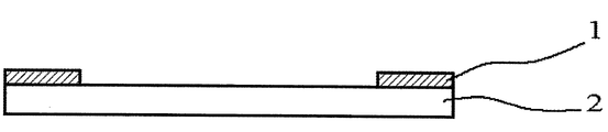
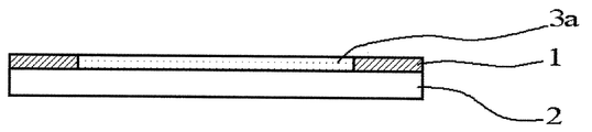
도 1b는 본 발명의 화상 표시 장치의 제조 방법의 공정 (A)의 설명도이다.
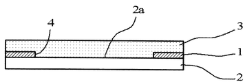
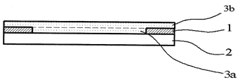
도 1c는 본 발명의 화상 표시 장치의 제조 방법의 공정 (B)의 설명도이다.
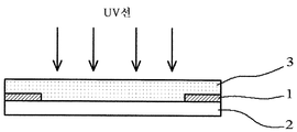
도 1d는 본 발명의 화상 표시 장치의 제조 방법의 공정 (B)의 설명도이다.
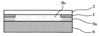
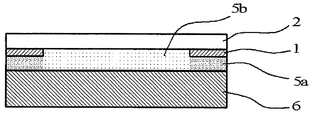
도 1e는 본 발명의 화상 표시 장치의 제조 방법의 공정 (C)의 설명도이다.
도 1f는 본 발명의 화상 표시 장치의 제조 방법의 공정 (D)의 설명도이다.
도 1g는 본 발명의 화상 표시 장치의 제조 방법의 공정 (D)의 설명도이다.
도 2a는 본 발명의 화상 표시 장치의 제조 방법의 공정 (AA)의 설명도이다.
도 2b는 본 발명의 화상 표시 장치의 제조 방법의 공정 (BB)의 설명도이다.
도 2c는 본 발명의 화상 표시 장치의 제조 방법의 공정 (BB)의 설명도이다.
도 2d는 본 발명의 화상 표시 장치의 제조 방법의 공정 (CC)의 설명도이다.
도 2e는 본 발명의 화상 표시 장치의 제조 방법의 공정 (DD)의 설명도이다.
도 2f는 본 발명의 화상 표시 장치의 제조 방법의 공정 (DD)의 설명도이다.
도 3a는 본 발명의 화상 표시 장치의 제조 방법의 공정 (a)의 설명도이다.
도 3b는 본 발명의 화상 표시 장치의 제조 방법의 공정 (a)의 설명도이다.
도 3c는 본 발명의 화상 표시 장치의 제조 방법의 공정 (b)의 설명도이다.
도 3d는 본 발명의 화상 표시 장치의 제조 방법의 공정 (b)의 설명도이다.
도 3e는 본 발명의 화상 표시 장치의 제조 방법의 공정 (c)의 설명도이다.
도 3f는 본 발명의 화상 표시 장치의 제조 방법의 공정 (c)의 설명도이다.
도 3g는 본 발명의 화상 표시 장치의 제조 방법의 공정 (d)의 설명도이다.
도 4a는 본 발명의 화상 표시 장치의 제조 방법의 공정 (aa)의 설명도이다.
도 4b는 본 발명의 화상 표시 장치의 제조 방법의 공정 (bb)의 설명도이다.
도 4c는 본 발명의 화상 표시 장치의 제조 방법의 공정 (bb)의 설명도이다.
도 4d는 본 발명의 화상 표시 장치의 제조 방법의 공정 (cc)의 설명도이다.
도 4e는 본 발명의 화상 표시 장치의 제조 방법의 공정 (dd)의 설명도이다.
도 4f는 본 발명의 화상 표시 장치의 제조 방법의 공정 (dd)의 설명도이다.
도 5는 광 투과성 경화 수지층의 접착 강도 시험의 설명도이다.
도 6a는 실시예 4에 있어서의 광 경화성 수지 조성물의 광 투과성 커버 부재에 대한 도포 형태의 설명도이다.
도 6b는 실시예 4에 있어서의 광 경화성 수지 조성물의 광 투과성 커버 부재에 대한 도포 형태의 설명도이다.
도 7은 비교예 1에 있어서의 광 경화성 수지 조성물의 광 투과성 커버 부재에 대한 도포 형태의 설명도이다.
도 8은 비교예 2에 있어서의 광 경화성 수지 조성물의 광 투과성 커버 부재에 대한 도포 형태의 설명도이다.
도 9는 비교예 3에 있어서의 광 경화성 수지 조성물의 광 투과성 커버 부재에 대한 도포 형태의 설명도이다.


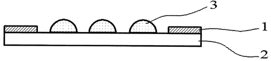
2: 광 투과성 커버 부재
2a: 광 투과성 커버 부재의 차광층 형성측 표면
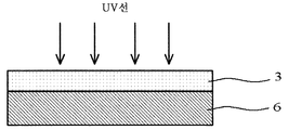
3, 3a, 3b: 광 경화성 수지 조성물
4: 단차
5, 5a, 5b: 가경화 수지층
6: 화상 표시 부재
7: 광 투과성 경화 수지층
10: 화상 표시 장치
20: 감쇠판
30: 유리 베이스
31: 유리판
Claims (9)
- 화상 표시 부재와, 주연부에 차광층이 형성된 광 투과성 커버 부재가 액상의 광 경화성 수지 조성물로부터 형성된 광 투과성 경화 수지층을 개재하여, 광 투과성 커버 부재의 차광층 형성면이 화상 표시 부재측에 배치되도록 적층된 화상 표시 장치의 제조 방법이며, 이하의 공정 (A) 내지 (D):
<공정 (A)>
액상의 광 경화성 수지 조성물을, 광 투과성 커버 부재의 차광층 형성측 표면 또는 화상 표시 부재의 표면에, 차광층과 광 투과성 커버 부재의 차광층 형성측 표면에서 형성되는 단차가 무효화되도록 차광층의 두께보다 두껍게 도포하는 공정;
<공정 (B)>
도포된 광 경화성 수지 조성물에 대하여 자외선을 조사하여 그의 경화율이 10 내지 80%가 되도록 가경화시킴으로써, 가경화 수지층을 형성하는 공정;
<공정 (C)>
화상 표시 부재에, 차광층과 가경화 수지층이 내측이 되도록 광 투과성 커버 부재를 접합하는 공정;
<공정 (D)>
화상 표시 부재와 광 투과성 커버 부재 사이에 협지되어 있는 가경화 수지층에 대하여 자외선을 조사하여 본경화시킴으로써, 화상 표시 부재와 광 투과성 커버 부재를 광 투과성 경화 수지층을 개재하여 적층시켜 화상 표시 장치를 얻는 공정
을 갖고, 상기 액상의 광 경화성 수지 조성물이, 이하의 성분 (가) 내지 (라):
<성분 (가)>
폴리이소프렌계 (메트)아크릴레이트올리고머, 폴리부타디엔계 (메트)아크릴레이트올리고머 및 폴리우레탄계 (메트)아크릴레이트올리고머로 이루어지는 군에서 선택되는 아크릴레이트계 올리고머 성분;
<성분 (나)>
아크릴계 단량체 성분;
<성분 (다)>
가소제 성분;
<성분 (라)>
광 중합 개시제 성분
을 함유하고, 성분 (가)와 성분 (나)의 광 경화성 수지 조성물 중에 있어서의 합계 함유량이 25 내지 80 질량%이며, 성분 (가)와 성분 (나) 사이의 질량비가 1:1 내지 2인 제조 방법. - 제1항에 있어서, 화상 표시 부재가 액정 표시 패널, 유기 EL 표시 패널, 플라즈마 표시 패널 또는 터치 패널인 제조 방법.
- 제1항에 있어서, 공정 (A)에서, 광 경화성 수지 조성물을 차광층 두께의 1.2 내지 50배의 두께로 도포하는 것인 제조 방법.
- 제1항에 있어서, 공정 (D)에서, 광 투과성 경화 수지층의 경화율이 90% 이상이 되도록 가경화 수지층에 자외선을 조사하여 본경화시키는 것인 제조 방법.
- 제1항에 있어서, 공정 (B)에서, 적어도 차광층 상에 위치하는 광 경화성 수지 조성물에 대하여 자외선을 조사하여 가경화시키고, 차광층 상의 가경화 수지층의 경화율을 30 내지 80%로 하는 것인 제조 방법.
- 제5항에 있어서, 공정 (B)에서, 광 투과성 커버 부재 표면의 가경화 수지층의 경화율이 0 내지 80%인 제조 방법.
- 제5항에 있어서, 공정 (B)에서, 차광층 상의 가경화 수지층의 경화율이 광 투과성 커버 부재 표면의 가경화 수지층의 경화율보다 높은 것인 제조 방법.
- 제5항에 있어서, 공정 (B)의 자외선 조사 시에, 자외선을 차폐하는 차폐판 또는 자외선을 감쇠시키는 감쇠판을, 자외선 광원과 도포된 광 경화성 수지 조성물 사이에 설치하는 것인 제조 방법.
- 제1항 내지 제8항 중 어느 한 항에 있어서, 가소제 성분이 고형의 점착 부여제와 액상 오일 성분을 함유하는 것인 제조 방법.
Priority Applications (1)
| Application Number | Priority Date | Filing Date | Title |
|---|---|---|---|
| KR1020207020936A KR102277736B1 (ko) | 2012-01-25 | 2013-01-24 | 화상 표시 장치의 제조 방법 |
Applications Claiming Priority (5)
| Application Number | Priority Date | Filing Date | Title |
|---|---|---|---|
| JP2012012904A JP5138820B1 (ja) | 2012-01-25 | 2012-01-25 | 画像表示装置の製造方法 |
| JPJP-P-2012-012904 | 2012-01-25 | ||
| JPJP-P-2012-273685 | 2012-12-14 | ||
| JP2012273685A JP6220123B2 (ja) | 2012-12-14 | 2012-12-14 | 画像表示装置の製造方法 |
| PCT/JP2013/051423 WO2013111810A1 (ja) | 2012-01-25 | 2013-01-24 | 画像表示装置の製造方法 |
Related Parent Applications (1)
| Application Number | Title | Priority Date | Filing Date |
|---|---|---|---|
| KR1020197012191A Division KR102097383B1 (ko) | 2012-01-25 | 2013-01-24 | 화상 표시 장치의 제조 방법 |
Related Child Applications (1)
| Application Number | Title | Priority Date | Filing Date |
|---|---|---|---|
| KR1020207020936A Division KR102277736B1 (ko) | 2012-01-25 | 2013-01-24 | 화상 표시 장치의 제조 방법 |
Publications (2)
| Publication Number | Publication Date |
|---|---|
| KR20200037443A true KR20200037443A (ko) | 2020-04-08 |
| KR102137449B1 KR102137449B1 (ko) | 2020-08-13 |
Family
ID=48873522
Family Applications (11)
| Application Number | Title | Priority Date | Filing Date |
|---|---|---|---|
| KR1020207020936A Active KR102277736B1 (ko) | 2012-01-25 | 2013-01-24 | 화상 표시 장치의 제조 방법 |
| KR1020237025526A Ceased KR20230114333A (ko) | 2012-01-25 | 2013-01-24 | 화상 표시 장치의 제조 방법 |
| KR1020227012822A Ceased KR20220054452A (ko) | 2012-01-25 | 2013-01-24 | 화상 표시 장치의 제조 방법 |
| KR1020167007679A Active KR101895136B1 (ko) | 2012-01-25 | 2013-01-24 | 화상 표시 장치의 제조 방법 |
| KR1020167013808A Active KR101895139B1 (ko) | 2012-01-25 | 2013-01-24 | 화상 표시 장치의 제조 방법 |
| KR1020137015229A Ceased KR20140145933A (ko) | 2012-01-25 | 2013-01-24 | 화상 표시 장치의 제조 방법 |
| KR1020197012191A Active KR102097383B1 (ko) | 2012-01-25 | 2013-01-24 | 화상 표시 장치의 제조 방법 |
| KR1020207009279A Active KR102137449B1 (ko) | 2012-01-25 | 2013-01-24 | 화상 표시 장치의 제조 방법 |
| KR1020217021562A Ceased KR20210090286A (ko) | 2012-01-25 | 2013-01-24 | 화상 표시 장치의 제조 방법 |
| KR1020147009273A Active KR101975622B1 (ko) | 2012-01-25 | 2013-01-24 | 화상 표시 장치의 제조 방법 |
| KR1020267002714A Pending KR20260036549A (ko) | 2012-01-25 | 2013-01-24 | 화상 표시 장치의 제조 방법 |
Family Applications Before (7)
| Application Number | Title | Priority Date | Filing Date |
|---|---|---|---|
| KR1020207020936A Active KR102277736B1 (ko) | 2012-01-25 | 2013-01-24 | 화상 표시 장치의 제조 방법 |
| KR1020237025526A Ceased KR20230114333A (ko) | 2012-01-25 | 2013-01-24 | 화상 표시 장치의 제조 방법 |
| KR1020227012822A Ceased KR20220054452A (ko) | 2012-01-25 | 2013-01-24 | 화상 표시 장치의 제조 방법 |
| KR1020167007679A Active KR101895136B1 (ko) | 2012-01-25 | 2013-01-24 | 화상 표시 장치의 제조 방법 |
| KR1020167013808A Active KR101895139B1 (ko) | 2012-01-25 | 2013-01-24 | 화상 표시 장치의 제조 방법 |
| KR1020137015229A Ceased KR20140145933A (ko) | 2012-01-25 | 2013-01-24 | 화상 표시 장치의 제조 방법 |
| KR1020197012191A Active KR102097383B1 (ko) | 2012-01-25 | 2013-01-24 | 화상 표시 장치의 제조 방법 |
Family Applications After (3)
| Application Number | Title | Priority Date | Filing Date |
|---|---|---|---|
| KR1020217021562A Ceased KR20210090286A (ko) | 2012-01-25 | 2013-01-24 | 화상 표시 장치의 제조 방법 |
| KR1020147009273A Active KR101975622B1 (ko) | 2012-01-25 | 2013-01-24 | 화상 표시 장치의 제조 방법 |
| KR1020267002714A Pending KR20260036549A (ko) | 2012-01-25 | 2013-01-24 | 화상 표시 장치의 제조 방법 |
Country Status (7)
| Country | Link |
|---|---|
| US (5) | US20140069581A1 (ko) |
| EP (2) | EP2680252B1 (ko) |
| KR (11) | KR102277736B1 (ko) |
| CN (8) | CN105807457B (ko) |
| HK (1) | HK1216564A1 (ko) |
| TW (7) | TWI671372B (ko) |
| WO (1) | WO2013111810A1 (ko) |
Families Citing this family (51)
| Publication number | Priority date | Publication date | Assignee | Title |
|---|---|---|---|---|
| CN105807457B (zh) * | 2012-01-25 | 2018-10-02 | 迪睿合电子材料有限公司 | 图像显示装置的制造方法 |
| HUE073469T2 (hu) | 2012-05-09 | 2026-01-28 | Dexerials Corp | Eljárás képmegjelenítõ készülék elõállítására |
| CN104768731B (zh) * | 2012-05-22 | 2018-06-19 | 汉高知识产权控股有限责任公司 | 用液态光学透明可光固化的粘合剂粘结基材的方法 |
| JP5994618B2 (ja) * | 2012-12-14 | 2016-09-21 | デクセリアルズ株式会社 | 光硬化性樹脂組成物及びそれを用いた画像表示装置の製造方法 |
| JP6378866B2 (ja) * | 2013-08-13 | 2018-08-22 | 富士通コンポーネント株式会社 | タッチパネルの製造方法 |
| DE112014003975B4 (de) * | 2013-08-30 | 2026-04-30 | Panasonic Housing Solutions Co., Ltd. | Anzeige-Vorrichtung und ein Herstellungsverfahren dafür |
| JP6390087B2 (ja) * | 2013-10-28 | 2018-09-19 | 三菱電機株式会社 | 表示装置及びその製造方法 |
| US10150279B2 (en) * | 2014-02-07 | 2018-12-11 | Htc Corporation | Panel laminating method, panel assembly and electronic device |
| JP6407535B2 (ja) * | 2014-02-28 | 2018-10-17 | ソマール株式会社 | 粘着シート及び被着体積層物の製造方法 |
| JP6324757B2 (ja) * | 2014-02-28 | 2018-05-16 | ソマール株式会社 | 粘着シート及び加工済み被着体の製造方法 |
| JP6407536B2 (ja) * | 2014-02-28 | 2018-10-17 | ソマール株式会社 | 粘着シート及び被着体積層物の製造方法 |
| JP6654278B2 (ja) * | 2014-06-10 | 2020-02-26 | 天馬微電子有限公司 | 機器及びその製造方法 |
| JP6404606B2 (ja) * | 2014-06-16 | 2018-10-10 | 平田機工株式会社 | 塗布方法、塗布装置、製造方法及び製造装置 |
| JP2016011976A (ja) * | 2014-06-27 | 2016-01-21 | 日本化薬株式会社 | 光学部材の製造方法及びそれに用いる紫外線硬化型樹脂組成物 |
| JP6499406B2 (ja) | 2014-06-30 | 2019-04-10 | 日本化薬株式会社 | 光学部材の製造方法及びそれに用いる硬化性樹脂組成物 |
| JP2016036780A (ja) * | 2014-08-08 | 2016-03-22 | 協立化学産業株式会社 | 積層体の製造方法 |
| CN104309267B (zh) * | 2014-09-17 | 2016-08-17 | 合肥鑫晟光电科技有限公司 | 一种基板贴合方法、触控显示基板、显示装置 |
| CN104290429A (zh) * | 2014-10-11 | 2015-01-21 | 合肥鑫晟光电科技有限公司 | 将显示面板与辅助面板相贴合的方法和显示装置 |
| US11208575B2 (en) | 2014-10-27 | 2021-12-28 | Illinois Tool Works Inc. | Assembly processes using UV curable pressure sensitive adhesives (PSA) or stageable PSA systems |
| JP6479589B2 (ja) * | 2015-06-22 | 2019-03-06 | デクセリアルズ株式会社 | 画像表示装置の製造方法 |
| JP6700004B2 (ja) | 2015-08-04 | 2020-05-27 | デクセリアルズ株式会社 | 光学部材の製造方法 |
| KR102331516B1 (ko) * | 2015-10-13 | 2021-11-25 | 동우 화인켐 주식회사 | 윈도우 필름 및 그의 제조방법 |
| CA3003689C (en) * | 2015-11-05 | 2023-10-10 | Tsk Laboratory Europe B.V. | Method for connecting two objects using a polymer composition and a system, for use in a cosmetic procedure |
| JP6623121B2 (ja) * | 2016-06-08 | 2019-12-18 | デクセリアルズ株式会社 | 光硬化性樹脂組成物、並びに画像表示装置、及びその製造方法 |
| KR102741535B1 (ko) * | 2016-09-13 | 2024-12-10 | 엘지디스플레이 주식회사 | 유기 발광 표시 장치 및 유기 발광 표시 장치 제조 방법 |
| JP6905325B2 (ja) * | 2016-10-31 | 2021-07-21 | デクセリアルズ株式会社 | 積層体の製造方法 |
| KR102617176B1 (ko) * | 2016-11-11 | 2023-12-21 | 엘지디스플레이 주식회사 | 커버 윈도우 및 이를 포함하는 표시장치 |
| KR102669729B1 (ko) * | 2016-11-17 | 2024-05-28 | 삼성디스플레이 주식회사 | 표시 장치 및 그 제조 방법 |
| WO2018146953A1 (ja) * | 2017-02-07 | 2018-08-16 | デクセリアルズ株式会社 | 画像表示装置の製造方法 |
| CN108538196A (zh) * | 2017-03-02 | 2018-09-14 | 元太科技工业股份有限公司 | 盖板结构及显示装置 |
| JP6834609B2 (ja) * | 2017-03-07 | 2021-02-24 | デクセリアルズ株式会社 | 画像表示装置の製造方法 |
| JP6878225B2 (ja) * | 2017-09-15 | 2021-05-26 | デクセリアルズ株式会社 | 透明パネルの製造方法、光学装置の製造方法 |
| CN111479693B (zh) | 2017-12-13 | 2023-06-16 | 3M创新有限公司 | 含有三烷基硼烷络合物引发剂和光酸的光学透明粘合剂 |
| JP6496901B2 (ja) * | 2018-06-21 | 2019-04-10 | 協立化学産業株式会社 | 積層体の製造方法 |
| KR102652773B1 (ko) * | 2018-12-13 | 2024-04-03 | 삼성디스플레이 주식회사 | 윈도우용 이형 필름 및 이의 제조 방법 |
| CN111587005A (zh) * | 2019-02-15 | 2020-08-25 | 致伸科技股份有限公司 | 壳体结构及其制造方法 |
| KR102622426B1 (ko) * | 2019-04-01 | 2024-01-09 | 삼성디스플레이 주식회사 | 표시장치용 윈도우, 이의 제조 방법 및 이를 포함하는 표시장치 |
| CN110164948B (zh) * | 2019-06-13 | 2021-12-28 | 京东方科技集团股份有限公司 | 一种像素界定层、制作方法和显示面板 |
| CN110752317A (zh) * | 2019-11-08 | 2020-02-04 | 深圳市华星光电半导体显示技术有限公司 | 显示面板及其制备方法 |
| CN110880562B (zh) * | 2019-11-29 | 2022-06-07 | 京东方科技集团股份有限公司 | 有机发光显示面板及制作方法、显示装置 |
| JP7705715B2 (ja) * | 2020-03-03 | 2025-07-10 | デクセリアルズ株式会社 | 画像表示装置の製造方法 |
| CN111391356A (zh) * | 2020-03-20 | 2020-07-10 | 东莞广华汽车饰件科技有限公司 | 一种透光皮革饰件的生产工艺 |
| CN111554698B (zh) * | 2020-03-27 | 2023-05-23 | 广州立景创新科技有限公司 | 图像获取组件及其制备方法 |
| JP7184843B2 (ja) * | 2020-04-30 | 2022-12-06 | デクセリアルズ株式会社 | 光学部材の製造方法 |
| CN111650765A (zh) * | 2020-05-09 | 2020-09-11 | 中国电子科技集团公司第五十五研究所 | 一种提高显示基板组水胶贴合可靠性和良品率的方法 |
| KR20220062209A (ko) | 2020-11-06 | 2022-05-16 | 삼성디스플레이 주식회사 | 수지 조성물, 접착 부재, 및 그 접착 부재를 포함하는 표시 장치 |
| TWI783482B (zh) * | 2021-05-13 | 2022-11-11 | 大陸商宸美(廈門)光電有限公司 | 觸控顯示裝置及其形成方法 |
| TWI796279B (zh) * | 2021-05-13 | 2023-03-11 | 大陸商宸美(廈門)光電有限公司 | 觸控顯示裝置及其形成方法 |
| CN114527606B (zh) * | 2022-03-02 | 2024-04-05 | 武汉华星光电技术有限公司 | 显示模组及显示装置 |
| TWI845054B (zh) * | 2022-12-07 | 2024-06-11 | 允昌國際有限公司 | 用於觸控顯示面板之塑料面板的製造方法及結構 |
| US20250353291A1 (en) * | 2024-05-15 | 2025-11-20 | Dupont Electronics, Inc. | Maintaining raw flexible plate integrity using pre-hardened flexible plate regions |
Citations (12)
| Publication number | Priority date | Publication date | Assignee | Title |
|---|---|---|---|---|
| WO2004108774A1 (ja) * | 2003-06-03 | 2004-12-16 | Konishi Co., Ltd. | 硬化性樹脂、その製造方法及び該硬化性樹脂を含む組成物 |
| WO2006016549A1 (ja) * | 2004-08-13 | 2006-02-16 | Lion Corporation | 毛髪化粧料 |
| JP2008126860A (ja) | 2006-11-21 | 2008-06-05 | Inoac Corp | エアバッグドア |
| WO2009054168A1 (ja) * | 2007-10-22 | 2009-04-30 | Sharp Kabushiki Kaisha | 表示装置及びその製造方法 |
| JP2009127023A (ja) * | 2007-11-28 | 2009-06-11 | Toagosei Co Ltd | 光硬化型粘接着剤製造用の光硬化型組成物及び光硬化型粘接着シート |
| JP2009186957A (ja) * | 2007-04-09 | 2009-08-20 | Sony Chemical & Information Device Corp | 樹脂組成物及び表示装置 |
| KR20100027041A (ko) | 2008-08-29 | 2010-03-10 | 도쿄엘렉트론가부시키가이샤 | 성막 장치, 성막 방법 및 기억 매체 |
| WO2010027041A1 (ja) * | 2008-09-05 | 2010-03-11 | 協立化学産業株式会社 | 光学機能材料を貼り合わせるための光硬化型樹脂組成物 |
| JP2010224094A (ja) * | 2009-03-23 | 2010-10-07 | Seiko Epson Corp | 電気光学装置の製造方法 |
| WO2011084405A1 (en) * | 2009-12-17 | 2011-07-14 | 3M Innovative Properties Company | Display panel assembly and methods of making same |
| JP2011145534A (ja) * | 2010-01-15 | 2011-07-28 | Hitachi Displays Ltd | フロントウインドウ付き表示装置およびその製造方法 |
| WO2011148990A1 (ja) * | 2010-05-26 | 2011-12-01 | 旭硝子株式会社 | 粘着層付き透明面材、表示装置およびそれらの製造方法 |
Family Cites Families (42)
| Publication number | Priority date | Publication date | Assignee | Title |
|---|---|---|---|---|
| JPH01101515A (ja) * | 1987-10-14 | 1989-04-19 | Matsushita Electric Ind Co Ltd | 液晶表示パネル |
| JPH0534516A (ja) * | 1991-07-26 | 1993-02-12 | A G Technol Kk | 表示装置用カラーフイルター |
| JPH06122856A (ja) * | 1992-10-09 | 1994-05-06 | Toyo Ink Mfg Co Ltd | 硬化性粘着テープもしくはシート |
| DE19741680C1 (de) * | 1997-09-22 | 1998-12-03 | Wkp Wuerttembergische Kunststo | Bahnförmige Matrize zum Erzeugen von Oberflächenmaterialien sowie Verfahren zum Herstellen einer solchen Matrize |
| KR100350425B1 (ko) * | 2000-04-04 | 2002-08-28 | 주식회사 일범 | 주철분말을 이용한 쾌속금형 제조방법 |
| US6798467B2 (en) * | 2000-12-21 | 2004-09-28 | Asahi Rubber Inc. | Liquid crystal display device and a method for producing the same |
| US7295280B2 (en) * | 2001-09-03 | 2007-11-13 | Hannstar Display Corp. | Method of manufacturing one drop fill liquid crystal display panel |
| JP3884351B2 (ja) * | 2002-08-26 | 2007-02-21 | 株式会社 日立ディスプレイズ | 画像表示装置およびその製造方法 |
| KR100590881B1 (ko) * | 2004-05-14 | 2006-06-19 | 삼성전자주식회사 | 광경화성 수지 조성물 및 그의 패터닝 방법 |
| EP1959417A4 (en) * | 2005-12-05 | 2009-11-11 | Seiko Instr Inc | DISPLAY AND DISPLAY MANUFACTURING METHOD |
| JP5217170B2 (ja) * | 2006-02-14 | 2013-06-19 | Dic株式会社 | 遮光性粘着テープ及びこれを用いたlcdモジュール |
| JP2007279554A (ja) * | 2006-04-11 | 2007-10-25 | Three M Innovative Properties Co | 液晶表示装置の保護ガラス用飛散防止膜 |
| JP4953717B2 (ja) * | 2006-05-19 | 2012-06-13 | リンテック株式会社 | 光学機能性フィルム貼合用粘着剤、光学機能性フィルム及びその製造方法 |
| CN103289025B (zh) * | 2006-07-14 | 2017-09-26 | 迪睿合电子材料有限公司 | 树脂组成物以及显示装置 |
| US8607102B2 (en) | 2006-09-15 | 2013-12-10 | Palo Alto Research Center Incorporated | Fault management for a printing system |
| JP2008088335A (ja) * | 2006-10-04 | 2008-04-17 | Sekisui Chem Co Ltd | 遮光用粘着テープ |
| EP2093594B1 (en) * | 2006-12-01 | 2013-01-09 | Kuraray Co., Ltd. | Pressure-sensitive adhesive for optical films |
| JP4978997B2 (ja) * | 2006-12-25 | 2012-07-18 | 株式会社ジャパンディスプレイイースト | 表示装置の製造方法 |
| KR101527980B1 (ko) * | 2007-04-03 | 2015-06-10 | 데쿠세리아루즈 가부시키가이샤 | 화상 표시 장치의 제조 방법 |
| JP2009186954A (ja) * | 2007-04-04 | 2009-08-20 | Sony Chemical & Information Device Corp | 画像表示装置の製造方法 |
| CN101681575B (zh) * | 2007-04-04 | 2013-10-30 | 索尼化学&信息部件株式会社 | 图像显示装置的制造方法 |
| JP5401824B2 (ja) * | 2007-04-09 | 2014-01-29 | デクセリアルズ株式会社 | 画像表示装置 |
| JP5138267B2 (ja) * | 2007-04-18 | 2013-02-06 | 日立化成工業株式会社 | プリプレグ、それを用いた多層基配線板及び電子部品 |
| CN100592170C (zh) * | 2007-05-25 | 2010-02-24 | 群康科技(深圳)有限公司 | 液晶显示装置及其制造方法 |
| JP4711354B2 (ja) * | 2007-07-17 | 2011-06-29 | ソニーケミカル&インフォメーションデバイス株式会社 | 画像表示装置の製造方法 |
| JP5343391B2 (ja) * | 2007-07-17 | 2013-11-13 | デクセリアルズ株式会社 | 樹脂組成物及び画像表示装置 |
| JP5295527B2 (ja) * | 2007-07-18 | 2013-09-18 | 協立化学産業株式会社 | 積層構造体の製造方法及びそれに使用する接着剤 |
| JP5115412B2 (ja) * | 2007-09-12 | 2013-01-09 | 日立化成工業株式会社 | 画像表示装置の製造方法及び画像表示装置 |
| JP5735279B2 (ja) * | 2007-12-28 | 2015-06-17 | イー・アイ・デュポン・ドウ・ヌムール・アンド・カンパニーE.I.Du Pont De Nemours And Company | 化学線硬化型接着剤組成物 |
| US20110033720A1 (en) * | 2008-04-11 | 2011-02-10 | Jun Fujita | Transparent adhesive sheet and image display device including the same |
| JP2010039684A (ja) | 2008-08-04 | 2010-02-18 | Canon Inc | 画像形成装置、情報処理装置、データ処理方法及びプログラム |
| JP2010067719A (ja) * | 2008-09-09 | 2010-03-25 | Tdk Corp | 積層セラミック電子部品の製造方法 |
| US8361632B2 (en) * | 2008-10-03 | 2013-01-29 | 3M Innovative Properties Company | Cloud point-resistant adhesives and laminates |
| CN102317398B (zh) * | 2009-02-16 | 2013-08-28 | 综研化学株式会社 | 光学构件用射线固化型粘合剂组合物以及粘合型光学构件 |
| JP5605088B2 (ja) | 2009-12-03 | 2014-10-15 | ソニー株式会社 | 液晶表示装置 |
| JP2011171372A (ja) * | 2010-02-16 | 2011-09-01 | Hitachi Cable Ltd | 配線基板の製造方法 |
| CN101867024B (zh) * | 2010-06-01 | 2011-10-05 | 友达光电股份有限公司 | 封装方法 |
| JP2012073533A (ja) * | 2010-09-29 | 2012-04-12 | Shibaura Mechatronics Corp | 貼合装置及び貼合方法 |
| JP5558993B2 (ja) * | 2010-09-29 | 2014-07-23 | 芝浦メカトロニクス株式会社 | 接着剤供給装置及び接着剤供給方法 |
| WO2012099171A1 (ja) * | 2011-01-18 | 2012-07-26 | シャープ株式会社 | 平面板付き表示パネル、平面板付き表示パネルの製造方法、及び、樹脂組成物 |
| MY170060A (en) * | 2011-10-21 | 2019-07-02 | Nippon Kayaku Kk | Method for producing optical member and use of ultraviolet ray cured resin composition for same |
| CN105807457B (zh) * | 2012-01-25 | 2018-10-02 | 迪睿合电子材料有限公司 | 图像显示装置的制造方法 |
-
2013
- 2013-01-24 CN CN201610333606.6A patent/CN105807457B/zh active Active
- 2013-01-24 EP EP13724717.7A patent/EP2680252B1/en active Active
- 2013-01-24 CN CN201380000424.1A patent/CN103403784B/zh active Active
- 2013-01-24 KR KR1020207020936A patent/KR102277736B1/ko active Active
- 2013-01-24 WO PCT/JP2013/051423 patent/WO2013111810A1/ja not_active Ceased
- 2013-01-24 CN CN201610333638.6A patent/CN105807468B/zh active Active
- 2013-01-24 KR KR1020237025526A patent/KR20230114333A/ko not_active Ceased
- 2013-01-24 KR KR1020227012822A patent/KR20220054452A/ko not_active Ceased
- 2013-01-24 CN CN201610333683.1A patent/CN105842894B/zh active Active
- 2013-01-24 CN CN201510966227.6A patent/CN105717741A/zh active Pending
- 2013-01-24 CN CN201510294461.9A patent/CN104992624B/zh active Active
- 2013-01-24 CN CN201610333640.3A patent/CN105807469B/zh active Active
- 2013-01-24 US US13/990,923 patent/US20140069581A1/en not_active Abandoned
- 2013-01-24 KR KR1020167007679A patent/KR101895136B1/ko active Active
- 2013-01-24 KR KR1020167013808A patent/KR101895139B1/ko active Active
- 2013-01-24 KR KR1020137015229A patent/KR20140145933A/ko not_active Ceased
- 2013-01-24 KR KR1020197012191A patent/KR102097383B1/ko active Active
- 2013-01-24 EP EP20178301.6A patent/EP3726283A1/en active Pending
- 2013-01-24 KR KR1020207009279A patent/KR102137449B1/ko active Active
- 2013-01-24 KR KR1020217021562A patent/KR20210090286A/ko not_active Ceased
- 2013-01-24 KR KR1020147009273A patent/KR101975622B1/ko active Active
- 2013-01-24 CN CN201410061256.3A patent/CN103927939B/zh active Active
- 2013-01-24 KR KR1020267002714A patent/KR20260036549A/ko active Pending
- 2013-01-25 TW TW107136026A patent/TWI671372B/zh active
- 2013-01-25 TW TW102102837A patent/TWI479202B/zh active
- 2013-01-25 TW TW107101076A patent/TWI641624B/zh active
- 2013-01-25 TW TW105140405A patent/TWI615411B/zh active
- 2013-01-25 TW TW102147730A patent/TWI440897B/zh active
- 2013-01-25 TW TW108120975A patent/TWI707934B/zh active
- 2013-01-25 TW TW103146233A patent/TWI567517B/zh active
-
2014
- 2014-09-15 US US14/486,354 patent/US10759156B2/en active Active
-
2016
- 2016-04-19 HK HK16104452.5A patent/HK1216564A1/zh unknown
-
2017
- 2017-10-30 US US15/797,937 patent/US10618267B2/en active Active
-
2019
- 2019-03-29 US US16/369,739 patent/US10843448B2/en active Active
-
2020
- 2020-10-23 US US17/078,830 patent/US11738548B2/en active Active
Patent Citations (13)
| Publication number | Priority date | Publication date | Assignee | Title |
|---|---|---|---|---|
| WO2004108774A1 (ja) * | 2003-06-03 | 2004-12-16 | Konishi Co., Ltd. | 硬化性樹脂、その製造方法及び該硬化性樹脂を含む組成物 |
| WO2006016549A1 (ja) * | 2004-08-13 | 2006-02-16 | Lion Corporation | 毛髪化粧料 |
| JP2008126860A (ja) | 2006-11-21 | 2008-06-05 | Inoac Corp | エアバッグドア |
| JP2009186957A (ja) * | 2007-04-09 | 2009-08-20 | Sony Chemical & Information Device Corp | 樹脂組成物及び表示装置 |
| US20100277684A1 (en) * | 2007-10-22 | 2010-11-04 | Hiroshi Fukushima | Display device and method for production thereof |
| WO2009054168A1 (ja) * | 2007-10-22 | 2009-04-30 | Sharp Kabushiki Kaisha | 表示装置及びその製造方法 |
| JP2009127023A (ja) * | 2007-11-28 | 2009-06-11 | Toagosei Co Ltd | 光硬化型粘接着剤製造用の光硬化型組成物及び光硬化型粘接着シート |
| KR20100027041A (ko) | 2008-08-29 | 2010-03-10 | 도쿄엘렉트론가부시키가이샤 | 성막 장치, 성막 방법 및 기억 매체 |
| WO2010027041A1 (ja) * | 2008-09-05 | 2010-03-11 | 協立化学産業株式会社 | 光学機能材料を貼り合わせるための光硬化型樹脂組成物 |
| JP2010224094A (ja) * | 2009-03-23 | 2010-10-07 | Seiko Epson Corp | 電気光学装置の製造方法 |
| WO2011084405A1 (en) * | 2009-12-17 | 2011-07-14 | 3M Innovative Properties Company | Display panel assembly and methods of making same |
| JP2011145534A (ja) * | 2010-01-15 | 2011-07-28 | Hitachi Displays Ltd | フロントウインドウ付き表示装置およびその製造方法 |
| WO2011148990A1 (ja) * | 2010-05-26 | 2011-12-01 | 旭硝子株式会社 | 粘着層付き透明面材、表示装置およびそれらの製造方法 |
Also Published As
Similar Documents
| Publication | Publication Date | Title |
|---|---|---|
| KR102097383B1 (ko) | 화상 표시 장치의 제조 방법 | |
| KR101483385B1 (ko) | 화상 표시 장치의 제조 방법 | |
| JP6220123B2 (ja) | 画像表示装置の製造方法 | |
| US20210107268A1 (en) | Method of manufacturing image display apparatus | |
| JP6975834B2 (ja) | 画像表示装置の製造方法 | |
| JP6786647B2 (ja) | 画像表示装置の製造方法 | |
| HK1191437B (en) | Image display device fabrication method |
Legal Events
| Date | Code | Title | Description |
|---|---|---|---|
| A107 | Divisional application of patent | ||
| PA0104 | Divisional application for international application |
St.27 status event code: A-0-1-A10-A18-div-PA0104 St.27 status event code: A-0-1-A10-A16-div-PA0104 |
|
| PA0201 | Request for examination |
St.27 status event code: A-1-2-D10-D11-exm-PA0201 |
|
| PG1501 | Laying open of application |
St.27 status event code: A-1-1-Q10-Q12-nap-PG1501 |
|
| E701 | Decision to grant or registration of patent right | ||
| PE0701 | Decision of registration |
St.27 status event code: A-1-2-D10-D22-exm-PE0701 |
|
| PA0104 | Divisional application for international application |
St.27 status event code: A-0-1-A10-A18-div-PA0104 St.27 status event code: A-0-1-A10-A16-div-PA0104 |
|
| GRNT | Written decision to grant | ||
| PR0701 | Registration of establishment |
St.27 status event code: A-2-4-F10-F11-exm-PR0701 |
|
| PR1002 | Payment of registration fee |
St.27 status event code: A-2-2-U10-U12-oth-PR1002 Fee payment year number: 1 |
|
| PG1601 | Publication of registration |
St.27 status event code: A-4-4-Q10-Q13-nap-PG1601 |
|
| R18-X000 | Changes to party contact information recorded |
St.27 status event code: A-5-5-R10-R18-oth-X000 |
|
| P22-X000 | Classification modified |
St.27 status event code: A-4-4-P10-P22-nap-X000 |
|
| P22-X000 | Classification modified |
St.27 status event code: A-4-4-P10-P22-nap-X000 |
|
| PR1001 | Payment of annual fee |
St.27 status event code: A-4-4-U10-U11-oth-PR1001 Fee payment year number: 4 |
|
| PR1001 | Payment of annual fee |
St.27 status event code: A-4-4-U10-U11-oth-PR1001 Fee payment year number: 5 |
|
| PR1001 | Payment of annual fee |
St.27 status event code: A-4-4-U10-U11-oth-PR1001 Fee payment year number: 6 |
|
| P22-X000 | Classification modified |
St.27 status event code: A-4-4-P10-P22-nap-X000 |