KR20200038531A - 기판 처리 장치, 반도체 장치의 제조 방법 및 프로그램 - Google Patents
기판 처리 장치, 반도체 장치의 제조 방법 및 프로그램 Download PDFInfo
- Publication number
- KR20200038531A KR20200038531A KR1020207007915A KR20207007915A KR20200038531A KR 20200038531 A KR20200038531 A KR 20200038531A KR 1020207007915 A KR1020207007915 A KR 1020207007915A KR 20207007915 A KR20207007915 A KR 20207007915A KR 20200038531 A KR20200038531 A KR 20200038531A
- Authority
- KR
- South Korea
- Prior art keywords
- substrate
- product
- substrates
- dummy
- loaded
- Prior art date
- Legal status (The legal status is an assumption and is not a legal conclusion. Google has not performed a legal analysis and makes no representation as to the accuracy of the status listed.)
- Granted
Links
Images


Classifications
-
- H01L21/67745—
-
- H—ELECTRICITY
- H10—SEMICONDUCTOR DEVICES; ELECTRIC SOLID-STATE DEVICES NOT OTHERWISE PROVIDED FOR
- H10P—GENERIC PROCESSES OR APPARATUS FOR THE MANUFACTURE OR TREATMENT OF DEVICES COVERED BY CLASS H10
- H10P72/00—Handling or holding of wafers, substrates or devices during manufacture or treatment thereof
- H10P72/30—Handling or holding of wafers, substrates or devices during manufacture or treatment thereof for conveying, e.g. between different workstations
- H10P72/33—Handling or holding of wafers, substrates or devices during manufacture or treatment thereof for conveying, e.g. between different workstations into and out of processing chamber
- H10P72/3304—Handling or holding of wafers, substrates or devices during manufacture or treatment thereof for conveying, e.g. between different workstations into and out of processing chamber characterised by movements or sequence of movements of transfer devices
-
- H—ELECTRICITY
- H10—SEMICONDUCTOR DEVICES; ELECTRIC SOLID-STATE DEVICES NOT OTHERWISE PROVIDED FOR
- H10P—GENERIC PROCESSES OR APPARATUS FOR THE MANUFACTURE OR TREATMENT OF DEVICES COVERED BY CLASS H10
- H10P72/00—Handling or holding of wafers, substrates or devices during manufacture or treatment thereof
- H10P72/30—Handling or holding of wafers, substrates or devices during manufacture or treatment thereof for conveying, e.g. between different workstations
- H10P72/33—Handling or holding of wafers, substrates or devices during manufacture or treatment thereof for conveying, e.g. between different workstations into and out of processing chamber
- H10P72/3302—Mechanical parts of transfer devices
-
- C—CHEMISTRY; METALLURGY
- C23—COATING METALLIC MATERIAL; COATING MATERIAL WITH METALLIC MATERIAL; CHEMICAL SURFACE TREATMENT; DIFFUSION TREATMENT OF METALLIC MATERIAL; COATING BY VACUUM EVAPORATION, BY SPUTTERING, BY ION IMPLANTATION OR BY CHEMICAL VAPOUR DEPOSITION, IN GENERAL; INHIBITING CORROSION OF METALLIC MATERIAL OR INCRUSTATION IN GENERAL
- C23C—COATING METALLIC MATERIAL; COATING MATERIAL WITH METALLIC MATERIAL; SURFACE TREATMENT OF METALLIC MATERIAL BY DIFFUSION INTO THE SURFACE, BY CHEMICAL CONVERSION OR SUBSTITUTION; COATING BY VACUUM EVAPORATION, BY SPUTTERING, BY ION IMPLANTATION OR BY CHEMICAL VAPOUR DEPOSITION, IN GENERAL
- C23C16/00—Chemical coating by decomposition of gaseous compounds, without leaving reaction products of surface material in the coating, i.e. chemical vapour deposition [CVD] processes
- C23C16/44—Chemical coating by decomposition of gaseous compounds, without leaving reaction products of surface material in the coating, i.e. chemical vapour deposition [CVD] processes characterised by the method of coating
- C23C16/458—Chemical coating by decomposition of gaseous compounds, without leaving reaction products of surface material in the coating, i.e. chemical vapour deposition [CVD] processes characterised by the method of coating characterised by the method used for supporting substrates in the reaction chamber
- C23C16/4582—Rigid and flat substrates, e.g. plates or discs
- C23C16/4583—Rigid and flat substrates, e.g. plates or discs the substrate being supported substantially horizontally
-
- G—PHYSICS
- G05—CONTROLLING; REGULATING
- G05B—CONTROL OR REGULATING SYSTEMS IN GENERAL; FUNCTIONAL ELEMENTS OF SUCH SYSTEMS; MONITORING OR TESTING ARRANGEMENTS FOR SUCH SYSTEMS OR ELEMENTS
- G05B19/00—Program-control systems
- G05B19/02—Program-control systems electric
- G05B19/418—Total factory control, i.e. centrally controlling a plurality of machines, e.g. direct or distributed numerical control [DNC], flexible manufacturing systems [FMS], integrated manufacturing systems [IMS] or computer integrated manufacturing [CIM]
-
- H01L21/67303—
-
- H01L21/67754—
-
- H01L21/67757—
-
- H—ELECTRICITY
- H10—SEMICONDUCTOR DEVICES; ELECTRIC SOLID-STATE DEVICES NOT OTHERWISE PROVIDED FOR
- H10P—GENERIC PROCESSES OR APPARATUS FOR THE MANUFACTURE OR TREATMENT OF DEVICES COVERED BY CLASS H10
- H10P32/00—Diffusion of dopants within, into or out of wafers, substrates or parts of devices
-
- H—ELECTRICITY
- H10—SEMICONDUCTOR DEVICES; ELECTRIC SOLID-STATE DEVICES NOT OTHERWISE PROVIDED FOR
- H10P—GENERIC PROCESSES OR APPARATUS FOR THE MANUFACTURE OR TREATMENT OF DEVICES COVERED BY CLASS H10
- H10P72/00—Handling or holding of wafers, substrates or devices during manufacture or treatment thereof
- H10P72/06—Apparatus for monitoring, sorting, marking, testing or measuring
- H10P72/0612—Production flow monitoring, e.g. for increasing throughput
-
- H—ELECTRICITY
- H10—SEMICONDUCTOR DEVICES; ELECTRIC SOLID-STATE DEVICES NOT OTHERWISE PROVIDED FOR
- H10P—GENERIC PROCESSES OR APPARATUS FOR THE MANUFACTURE OR TREATMENT OF DEVICES COVERED BY CLASS H10
- H10P72/00—Handling or holding of wafers, substrates or devices during manufacture or treatment thereof
- H10P72/10—Handling or holding of wafers, substrates or devices during manufacture or treatment thereof using carriers specially adapted therefor, e.g. front opening unified pods [FOUP]
- H10P72/12—Vertical boat type carrier whereby the substrates are horizontally supported, e.g. comprising rod-shaped elements
-
- H—ELECTRICITY
- H10—SEMICONDUCTOR DEVICES; ELECTRIC SOLID-STATE DEVICES NOT OTHERWISE PROVIDED FOR
- H10P—GENERIC PROCESSES OR APPARATUS FOR THE MANUFACTURE OR TREATMENT OF DEVICES COVERED BY CLASS H10
- H10P72/00—Handling or holding of wafers, substrates or devices during manufacture or treatment thereof
- H10P72/30—Handling or holding of wafers, substrates or devices during manufacture or treatment thereof for conveying, e.g. between different workstations
- H10P72/33—Handling or holding of wafers, substrates or devices during manufacture or treatment thereof for conveying, e.g. between different workstations into and out of processing chamber
- H10P72/3311—Horizontal transfer of a batch of workpieces
-
- H—ELECTRICITY
- H10—SEMICONDUCTOR DEVICES; ELECTRIC SOLID-STATE DEVICES NOT OTHERWISE PROVIDED FOR
- H10P—GENERIC PROCESSES OR APPARATUS FOR THE MANUFACTURE OR TREATMENT OF DEVICES COVERED BY CLASS H10
- H10P72/00—Handling or holding of wafers, substrates or devices during manufacture or treatment thereof
- H10P72/30—Handling or holding of wafers, substrates or devices during manufacture or treatment thereof for conveying, e.g. between different workstations
- H10P72/33—Handling or holding of wafers, substrates or devices during manufacture or treatment thereof for conveying, e.g. between different workstations into and out of processing chamber
- H10P72/3312—Vertical transfer of a batch of workpieces
-
- H—ELECTRICITY
- H10—SEMICONDUCTOR DEVICES; ELECTRIC SOLID-STATE DEVICES NOT OTHERWISE PROVIDED FOR
- H10P—GENERIC PROCESSES OR APPARATUS FOR THE MANUFACTURE OR TREATMENT OF DEVICES COVERED BY CLASS H10
- H10P72/00—Handling or holding of wafers, substrates or devices during manufacture or treatment thereof
- H10P72/30—Handling or holding of wafers, substrates or devices during manufacture or treatment thereof for conveying, e.g. between different workstations
- H10P72/34—Handling or holding of wafers, substrates or devices during manufacture or treatment thereof for conveying, e.g. between different workstations the wafers being stored in a carrier, involving loading and unloading
- H10P72/3411—Handling or holding of wafers, substrates or devices during manufacture or treatment thereof for conveying, e.g. between different workstations the wafers being stored in a carrier, involving loading and unloading involving loading and unloading of wafers
- H10P72/3412—Batch transfer of wafers
-
- H—ELECTRICITY
- H10—SEMICONDUCTOR DEVICES; ELECTRIC SOLID-STATE DEVICES NOT OTHERWISE PROVIDED FOR
- H10P—GENERIC PROCESSES OR APPARATUS FOR THE MANUFACTURE OR TREATMENT OF DEVICES COVERED BY CLASS H10
- H10P90/00—Preparation of wafers not covered by a single main group of this subclass, e.g. wafer reinforcement
- H10P90/12—Preparing bulk and homogeneous wafers
Landscapes
- Chemical & Material Sciences (AREA)
- Engineering & Computer Science (AREA)
- Metallurgy (AREA)
- Chemical Kinetics & Catalysis (AREA)
- Organic Chemistry (AREA)
- Mechanical Engineering (AREA)
- Automation & Control Theory (AREA)
- Materials Engineering (AREA)
- General Chemical & Material Sciences (AREA)
- Quality & Reliability (AREA)
- Manufacturing & Machinery (AREA)
- General Physics & Mathematics (AREA)
- General Engineering & Computer Science (AREA)
- Physics & Mathematics (AREA)
- Chemical Vapour Deposition (AREA)
- Container, Conveyance, Adherence, Positioning, Of Wafer (AREA)
- Robotics (AREA)
Abstract
Description
도 2는 본 발명의 실시 형태에 관한 기판 처리 장치의 측면 투시도이다.
도 3은 본 발명의 실시 형태에 관한 기판 처리 장치의 처리로의 평면도이다.
도 4는 도 1의 A-A선에서의 수직 단면도이다.
도 5는 본 발명의 실시 형태에 관한 컨트롤러 구성의 도시 예이다.
도 6은 본 발명의 실시 형태에 관한 기판 처리 공정을 나타내는 흐름도이다.
도 7은 본 발명의 실시 형태에 관한 기판 처리 시퀀스를 나타내는 흐름도이다.
도 8은 본 발명의 실시 형태에 관한 기판 배치 프로그램을 나타내는 흐름도이다.
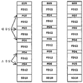
도 9는 본 발명의 실시 형태에 관한 모니터 웨이퍼의 이동 탑재 패턴을 설명하기 위한 도면이다.
도 10은 본 발명의 실시 형태에 관한 기판 배치 프로그램의 구체예를 도시하는 도면이다.
도 11은 본 발명의 실시 형태에 관한 기판 배치 프로그램의 실시예를 도시하는 도면이다.
도 12는 본 발명의 실시 형태에 관한 기판 배치 프로그램의 실시예를 도시하는 도면이다.
도 13은 본 발명의 실시 형태에 관한 기판 처리 시퀀스에서의 효과를 도시하는 도면이다.
217: 보트(기판 보유 지지구)
Claims (11)
- 제품 기판과 더미 기판을 포함하는 복수매의 각종 기판을 보유 지지하는 기판 보유 지지구와, 상기 각종 기판을 상기 기판 보유 지지구에 장전하는 이동 탑재 기구와, 상기 기판 보유 지지구에 적재 가능한 기판 매수와, 상기 기판 보유 지지구에 적재되는 상기 제품 기판의 매수를 취득하고, 취득한 상기 제품 기판의 매수로부터 상기 제품 기판을 복수의 기판 군으로 분할하고, 취득한 상기 제품 기판의 매수와 상기 기판 보유 지지구에 적재 가능한 기판 매수, 및 상기 제품 기판의 기판 군의 수에 기초하여 상기 더미 기판을 복수의 기판 군으로 분할하고, 상기 제품 기판의 기판 군과 상기 더미 기판의 기판 군을 조합하여, 상기 기판 보유 지지구의 복수의 영역에 상기 제품 기판을 분산시켜 적재하는 기판 배치 데이터를 작성하고, 작성된 기판 배치 데이터에 따라, 상기 각종 기판을 상기 이동 탑재 기구로 상기 기판 보유 지지구에 이동 탑재시키는 제어부를 구비한 기판 처리 장치.
- 제1항에 있어서, 상기 이동 탑재 기구는, 상기 각종 기판 N매를 일괄적으로 반송 가능하게 구성되어 있고, 상기 제어부는, 취득한 상기 제품 기판의 매수에 따라, 상기 제품 기판 N매와 상기 제품 기판 N-1매의 기판 군으로 복수 분할하여, 분할된 기판 군을 상기 기판 보유 지지부의 복수의 영역에 이동 탑재하도록 상기 기판 배치 데이터를 작성하도록 구성되어 있는, 기판 처리 장치.
- 제1항에 있어서, 상기 제어부는, 상기 기판 보유 지지구에 적재 가능한 기판 매수와 상기 기판 보유 지지구에 적재되는 상기 제품 기판의 매수로부터 상기 더미 기판의 매수를 산출하고, 산출된 상기 더미 기판의 매수에 기초하여 상기 더미 기판의 기판 군을 작성하도록 구성되어 있는, 기판 처리 장치.
- 제3항에 있어서, 상기 제어부는, 상기 더미 기판의 기판 군을 상기 제품 기판의 기판 군의 사이에 배치하도록, 상기 기판 배치 데이터를 작성하도록 구성되어 있는, 기판 처리 장치.
- 제3항에 있어서, 상기 제어부는, 상기 더미 기판의 기판 군의 수를, 상기 제품 기판의 기판 군의 수보다 많게 작성하도록 구성되어 있는, 기판 처리 장치.
- 제3항에 있어서, 상기 제어부는, 상기 제품 기판의 기판 군 중 양단에 배치된 기판 군의 외측에, 상기 더미 기판의 기판 군을 배치하도록 구성되어 있는, 기판 처리 장치.
- 제1항에 있어서, 상기 제품 기판은, 20매 이상이고 100매 이하인, 기판 처리 장치.
- 제2항에 있어서, 상기 제품 기판의 기판 군은, 제품 기판이 5매 이하로 구성되는, 기판 처리 장치.
- 제1항에 있어서, 상기 제어부는, 모니터 기판을 상기 기판 보유 지지구에 장전하는 이동 탑재 패턴을 설정하는 설정 화면을 갖고, 상기 설정 화면 상에서, 상기 기판 보유 지지구의 상하단에 장전하는 상기 모니터 기판의 매수와, 상기 기판 보유 지지구의 기판 보유 지지 영역에 장전하는 상기 모니터 기판의 매수를, 각각 설정 가능하게 구성되어 있는, 기판 처리 장치.
- 제품 기판과 더미 기판을 포함하는 복수매의 각종 기판을 보유 지지하는 기판 보유 지지구에 적재 가능한 기판 매수와, 상기 기판 보유 지지구에 적재되는 상기 제품 기판의 매수를 취득하고, 취득한 상기 제품 기판의 매수로부터 상기 제품 기판을 복수의 기판 군으로 분할하고, 취득한 상기 제품 기판의 매수와 상기 기판 보유 지지구에 적재 가능한 기판 매수, 및 상기 제품 기판의 기판 군의 수에 기초하여 상기 더미 기판을 복수의 기판 군으로 분할하고, 상기 제품 기판의 기판 군과 상기 더미 기판의 기판 군을 조합하여, 상기 기판 보유 지지구의 복수의 영역에 상기 제품 기판을 분산시켜 적재하는 기판 배치 데이터를 작성하는 공정과, 상기 기판 배치 데이터에 기초하여 상기 각종 기판을 상기 기판 보유 지지구에 이동 탑재하는 공정과, 상기 기판 보유 지지구를 로 내에 장입해서 상기 제품 기판을 처리하는 공정을 갖는 반도체 장치의 제조 방법.
- 제품 기판과 더미 기판을 포함하는 복수매의 각종 기판을 보유 지지하는 기판 보유 지지구와, 상기 기판을 상기 기판 보유 지지구에 장전하는 이동 탑재 기구와, 상기 각종 기판을 상기 기판 보유 지지구에 이동 탑재시키도록 상기 이동 탑재 기구를 제어하도록 구성되어 있는 제어부를 구비한 기판 처리 장치에서 실행되는 프로그램이며, 상기 제어부에, 상기 기판 보유 지지구에 적재 가능한 기판 매수와, 상기 기판 보유 지지구에 적재되는 상기 제품 기판의 매수를 취득하고, 취득한 상기 제품 기판의 매수로부터 상기 제품 기판을 복수의 기판 군으로 분할하고, 취득한 상기 제품 기판의 매수와 상기 기판 보유 지지구에 적재 가능한 기판 매수, 및 상기 제품 기판의 기판 군의 수에 기초하여 상기 더미 기판을 복수의 기판 군으로 분할하고, 상기 제품 기판의 기판 군과 상기 더미 기판의 기판 군을 조합하여, 상기 기판 보유 지지구의 복수의 영역에 상기 제품 기판을 분산시켜 적재하는 기판 배치 데이터를 작성시키는 수순과, 작성된 상기 기판 배치 데이터에 따라, 상기 기판을 상기 이동 탑재 기구에 이동 탑재시키는 수순을 실행시키는 프로그램.
Applications Claiming Priority (1)
| Application Number | Priority Date | Filing Date | Title |
|---|---|---|---|
| PCT/JP2017/035004 WO2019064384A1 (ja) | 2017-09-27 | 2017-09-27 | 基板処理装置、半導体装置の製造方法及びプログラム |
Publications (2)
| Publication Number | Publication Date |
|---|---|
| KR20200038531A true KR20200038531A (ko) | 2020-04-13 |
| KR102384558B1 KR102384558B1 (ko) | 2022-04-08 |
Family
ID=65903249
Family Applications (1)
| Application Number | Title | Priority Date | Filing Date |
|---|---|---|---|
| KR1020207007915A Active KR102384558B1 (ko) | 2017-09-27 | 2017-09-27 | 기판 처리 장치, 반도체 장치의 제조 방법 및 프로그램 |
Country Status (6)
| Country | Link |
|---|---|
| US (1) | US11876010B2 (ko) |
| JP (1) | JP6784848B2 (ko) |
| KR (1) | KR102384558B1 (ko) |
| CN (1) | CN111033714B (ko) |
| TW (1) | TWI720335B (ko) |
| WO (1) | WO2019064384A1 (ko) |
Families Citing this family (4)
| Publication number | Priority date | Publication date | Assignee | Title |
|---|---|---|---|---|
| KR20210044849A (ko) * | 2018-09-20 | 2021-04-23 | 가부시키가이샤 코쿠사이 엘렉트릭 | 기판 처리 장치, 반도체 장치의 제조 방법 및 프로그램 |
| JP7175210B2 (ja) * | 2019-02-04 | 2022-11-18 | 東京エレクトロン株式会社 | 排気装置、処理システム及び処理方法 |
| CN115244650B (zh) * | 2020-03-06 | 2025-10-14 | 株式会社尼康 | 控制装置、控制方法以及程序 |
| JP7706554B2 (ja) * | 2021-08-02 | 2025-07-11 | 株式会社Kokusai Electric | 基板処理装置、基板処理方法およびプログラム |
Citations (6)
| Publication number | Priority date | Publication date | Assignee | Title |
|---|---|---|---|---|
| JPH08306601A (ja) * | 1995-05-01 | 1996-11-22 | Tokyo Electron Ltd | 処理方法及び処理装置 |
| JPH098100A (ja) * | 1995-06-23 | 1997-01-10 | Tokyo Electron Ltd | 熱処理装置 |
| JPH10125761A (ja) | 1996-10-22 | 1998-05-15 | Kokusai Electric Co Ltd | 基板移載装置及び基板移載方法 |
| JPH10256341A (ja) | 1997-03-06 | 1998-09-25 | Kokusai Electric Co Ltd | 半導体製造装置 |
| KR20040019386A (ko) * | 2001-08-08 | 2004-03-05 | 동경 엘렉트론 주식회사 | 열처리방법 및 열처리장치 |
| JP2006339660A (ja) * | 2006-06-08 | 2006-12-14 | Hitachi Kokusai Electric Inc | 縦型拡散/cvd装置及びウェーハ移載方法 |
Family Cites Families (24)
| Publication number | Priority date | Publication date | Assignee | Title |
|---|---|---|---|---|
| KR970011656B1 (ko) * | 1988-02-25 | 1997-07-12 | 도오교오 에레구토론 사가미 가부시끼가이샤 | 웨이퍼 이동 교체 방법 |
| US5217340A (en) * | 1989-01-28 | 1993-06-08 | Kokusai Electric Co., Ltd. | Wafer transfer mechanism in vertical CVD diffusion apparatus |
| JPH07105357B2 (ja) * | 1989-01-28 | 1995-11-13 | 国際電気株式会社 | 縦型cvd拡散装置に於けるウェーハ移載方法及び装置 |
| JP3594090B2 (ja) * | 1992-09-09 | 2004-11-24 | 株式会社日立国際電気 | 縦型拡散/cvd装置及びウェーハ移載方法 |
| US5942012A (en) * | 1995-06-09 | 1999-08-24 | Tokyo Electron Limited | Heat treatment apparatus |
| JP4232307B2 (ja) * | 1999-03-23 | 2009-03-04 | 東京エレクトロン株式会社 | バッチ式熱処理装置の運用方法 |
| JP4342745B2 (ja) * | 2000-09-27 | 2009-10-14 | 株式会社日立国際電気 | 基板処理方法および半導体装置の製造方法 |
| JP3400996B1 (ja) * | 2001-11-02 | 2003-04-28 | 東京エレクトロン株式会社 | 熱処理装置及び熱処理方法 |
| JP3835751B2 (ja) * | 2002-06-14 | 2006-10-18 | 株式会社日立国際電気 | 縦型拡散/cvd装置及びウェーハ移載方法 |
| JP4030858B2 (ja) * | 2002-10-30 | 2008-01-09 | 東京エレクトロン株式会社 | 熱処理装置及び熱処理方法 |
| KR100609065B1 (ko) * | 2004-08-04 | 2006-08-10 | 삼성전자주식회사 | 산화막 형성 장치 및 방법 |
| KR100594470B1 (ko) * | 2004-12-29 | 2006-06-30 | 동부일렉트로닉스 주식회사 | 연속 공정이 가능한 반도체 제조 설비 |
| JP5420850B2 (ja) * | 2008-03-25 | 2014-02-19 | 株式会社日立国際電気 | 基板処理装置、基板処理システムおよび半導体装置の製造方法 |
| JP5166138B2 (ja) * | 2008-07-02 | 2013-03-21 | パナソニック株式会社 | 半導体装置の製造方法および半導体装置の製造装置 |
| JP6026801B2 (ja) * | 2011-10-19 | 2016-11-16 | 株式会社日立国際電気 | 基板処理装置、基板搬送方法及び半導体装置の製造方法 |
| JP6301083B2 (ja) * | 2012-09-12 | 2018-03-28 | 株式会社日立国際電気 | 基板処理装置、半導体装置の製造方法、及びレシピの作成方法 |
| CN104934317B (zh) * | 2014-03-20 | 2019-04-23 | 中芯国际集成电路制造(上海)有限公司 | 一种晶片生长装置及方法 |
| US9228260B1 (en) * | 2014-07-30 | 2016-01-05 | Taiwan Semiconductor Manufacturing Co., Ltd. | Wafer processing chamber, heat treatment apparatus and method for processing wafers |
| JP6531743B2 (ja) * | 2016-09-27 | 2019-06-19 | 信越半導体株式会社 | 貼り合わせsoiウェーハの製造方法 |
| US10373818B1 (en) * | 2018-01-31 | 2019-08-06 | Taiwan Semiconductor Manufacturing Co., Ltd. | Method of wafer recycling |
| KR20190109216A (ko) * | 2018-03-15 | 2019-09-25 | 가부시키가이샤 코쿠사이 엘렉트릭 | 기판 처리 장치 및 반도체 장치의 제조 방법 |
| US11121014B2 (en) * | 2018-06-05 | 2021-09-14 | Asm Ip Holding B.V. | Dummy wafer storage cassette |
| CN113508455B (zh) * | 2019-03-22 | 2024-03-26 | 株式会社国际电气 | 基板处理装置、半导体器件的制造方法以及记录介质 |
| JP7400683B2 (ja) * | 2020-10-07 | 2023-12-19 | 株式会社Sumco | 横型熱処理炉を用いたシリコンウェーハの熱処理方法 |
-
2017
- 2017-09-27 JP JP2019545455A patent/JP6784848B2/ja active Active
- 2017-09-27 KR KR1020207007915A patent/KR102384558B1/ko active Active
- 2017-09-27 CN CN201780094084.1A patent/CN111033714B/zh active Active
- 2017-09-27 WO PCT/JP2017/035004 patent/WO2019064384A1/ja not_active Ceased
-
2018
- 2018-08-27 TW TW107129748A patent/TWI720335B/zh active
-
2020
- 2020-03-17 US US16/821,563 patent/US11876010B2/en active Active
Patent Citations (6)
| Publication number | Priority date | Publication date | Assignee | Title |
|---|---|---|---|---|
| JPH08306601A (ja) * | 1995-05-01 | 1996-11-22 | Tokyo Electron Ltd | 処理方法及び処理装置 |
| JPH098100A (ja) * | 1995-06-23 | 1997-01-10 | Tokyo Electron Ltd | 熱処理装置 |
| JPH10125761A (ja) | 1996-10-22 | 1998-05-15 | Kokusai Electric Co Ltd | 基板移載装置及び基板移載方法 |
| JPH10256341A (ja) | 1997-03-06 | 1998-09-25 | Kokusai Electric Co Ltd | 半導体製造装置 |
| KR20040019386A (ko) * | 2001-08-08 | 2004-03-05 | 동경 엘렉트론 주식회사 | 열처리방법 및 열처리장치 |
| JP2006339660A (ja) * | 2006-06-08 | 2006-12-14 | Hitachi Kokusai Electric Inc | 縦型拡散/cvd装置及びウェーハ移載方法 |
Also Published As
| Publication number | Publication date |
|---|---|
| US11876010B2 (en) | 2024-01-16 |
| JP6784848B2 (ja) | 2020-11-11 |
| US20200219745A1 (en) | 2020-07-09 |
| CN111033714B (zh) | 2023-12-29 |
| TW201933517A (zh) | 2019-08-16 |
| CN111033714A (zh) | 2020-04-17 |
| TWI720335B (zh) | 2021-03-01 |
| WO2019064384A1 (ja) | 2019-04-04 |
| KR102384558B1 (ko) | 2022-04-08 |
| JPWO2019064384A1 (ja) | 2020-03-26 |
Similar Documents
| Publication | Publication Date | Title |
|---|---|---|
| KR102207673B1 (ko) | 성막 장치, 성막 방법 및 단열 부재 | |
| US9695509B2 (en) | Substrate processing apparatus, purging apparatus, method of manufacturing semiconductor device, and recording medium | |
| KR101089337B1 (ko) | 반도체 장치의 제조 방법 | |
| US11094572B2 (en) | Substrate processing apparatus and recording medium | |
| JP5902073B2 (ja) | 半導体装置の製造方法、基板処理方法及び基板処理装置 | |
| JP6061545B2 (ja) | 半導体装置の製造方法、基板処理方法および基板処理装置 | |
| US11876010B2 (en) | Substrate processing apparatus and recording medium | |
| JP2008258595A (ja) | 基板処理装置 | |
| US11031270B2 (en) | Substrate processing apparatus, substrate holder and mounting tool | |
| JP6301083B2 (ja) | 基板処理装置、半導体装置の製造方法、及びレシピの作成方法 | |
| KR20120095297A (ko) | 반도체 장치의 제조 방법 및 기판 처리 장치 | |
| JP2014067796A5 (ko) | ||
| KR20180100630A (ko) | 반도체 장치의 제조 방법, 기판 장전 방법 및 기록 매체 | |
| KR102111210B1 (ko) | 반도체 장치의 제조 방법, 기판 처리 장치 및 기록매체 | |
| KR102206194B1 (ko) | 기판 처리 장치 및 반도체 장치의 제조 방법 | |
| JP7030772B2 (ja) | 基板処理装置、半導体装置の製造方法及びプログラム | |
| KR20210127738A (ko) | 반도체 장치의 제조 방법, 기판 처리 장치 및 프로그램 | |
| JP2019114784A (ja) | 基板処理装置、半導体装置の製造方法及びプログラム | |
| WO2022064882A1 (ja) | 基板配置データの表示方法、半導体装置の製造方法及び基板処理装置並びにプログラム | |
| JP2012009744A (ja) | 基板処理装置 | |
| JP2013045862A (ja) | 基板処理システム | |
| JP2013239656A (ja) | 基板処理装置 | |
| JP2001338883A (ja) | 半導体装置の製造方法 | |
| KR20250144889A (ko) | 기판 처리 방법, 반도체 장치의 제조 방법, 기판 처리 장치 및 프로그램 | |
| KR20200108782A (ko) | 성막 장치 및 성막 방법 |
Legal Events
| Date | Code | Title | Description |
|---|---|---|---|
| P11-X000 | Amendment of application requested |
St.27 status event code: A-2-2-P10-P11-nap-X000 |
|
| P13-X000 | Application amended |
St.27 status event code: A-2-2-P10-P13-nap-X000 |
|
| PA0105 | International application |
St.27 status event code: A-0-1-A10-A15-nap-PA0105 |
|
| PA0201 | Request for examination |
St.27 status event code: A-1-2-D10-D11-exm-PA0201 |
|
| PG1501 | Laying open of application |
St.27 status event code: A-1-1-Q10-Q12-nap-PG1501 |
|
| E902 | Notification of reason for refusal | ||
| PE0902 | Notice of grounds for rejection |
St.27 status event code: A-1-2-D10-D21-exm-PE0902 |
|
| P11-X000 | Amendment of application requested |
St.27 status event code: A-2-2-P10-P11-nap-X000 |
|
| P13-X000 | Application amended |
St.27 status event code: A-2-2-P10-P13-nap-X000 |
|
| E701 | Decision to grant or registration of patent right | ||
| PE0701 | Decision of registration |
St.27 status event code: A-1-2-D10-D22-exm-PE0701 |
|
| GRNT | Written decision to grant | ||
| PR0701 | Registration of establishment |
St.27 status event code: A-2-4-F10-F11-exm-PR0701 |
|
| PR1002 | Payment of registration fee |
St.27 status event code: A-2-2-U10-U12-oth-PR1002 Fee payment year number: 1 |
|
| PG1601 | Publication of registration |
St.27 status event code: A-4-4-Q10-Q13-nap-PG1601 |
|
| P22-X000 | Classification modified |
St.27 status event code: A-4-4-P10-P22-nap-X000 |
|
| R18 | Changes to party contact information recorded |
Free format text: ST27 STATUS EVENT CODE: A-5-5-R10-R18-OTH-X000 (AS PROVIDED BY THE NATIONAL OFFICE) |
|
| R18-X000 | Changes to party contact information recorded |
St.27 status event code: A-5-5-R10-R18-oth-X000 |