KR20200043906A - 웨이퍼의 가공 방법 - Google Patents
웨이퍼의 가공 방법 Download PDFInfo
- Publication number
- KR20200043906A KR20200043906A KR1020190125325A KR20190125325A KR20200043906A KR 20200043906 A KR20200043906 A KR 20200043906A KR 1020190125325 A KR1020190125325 A KR 1020190125325A KR 20190125325 A KR20190125325 A KR 20190125325A KR 20200043906 A KR20200043906 A KR 20200043906A
- Authority
- KR
- South Korea
- Prior art keywords
- wafer
- polyolefin
- sheet
- frame
- based sheet
- Prior art date
- Legal status (The legal status is an assumption and is not a legal conclusion. Google has not performed a legal analysis and makes no representation as to the accuracy of the status listed.)
- Granted
Links
Images




Classifications
-
- H01L21/78—
-
- H—ELECTRICITY
- H10—SEMICONDUCTOR DEVICES; ELECTRIC SOLID-STATE DEVICES NOT OTHERWISE PROVIDED FOR
- H10P—GENERIC PROCESSES OR APPARATUS FOR THE MANUFACTURE OR TREATMENT OF DEVICES COVERED BY CLASS H10
- H10P72/00—Handling or holding of wafers, substrates or devices during manufacture or treatment thereof
- H10P72/70—Handling or holding of wafers, substrates or devices during manufacture or treatment thereof for supporting or gripping
- H10P72/78—Handling or holding of wafers, substrates or devices during manufacture or treatment thereof for supporting or gripping using vacuum or suction, e.g. Bernoulli chucks
-
- H—ELECTRICITY
- H10—SEMICONDUCTOR DEVICES; ELECTRIC SOLID-STATE DEVICES NOT OTHERWISE PROVIDED FOR
- H10P—GENERIC PROCESSES OR APPARATUS FOR THE MANUFACTURE OR TREATMENT OF DEVICES COVERED BY CLASS H10
- H10P72/00—Handling or holding of wafers, substrates or devices during manufacture or treatment thereof
- H10P72/70—Handling or holding of wafers, substrates or devices during manufacture or treatment thereof for supporting or gripping
- H10P72/74—Handling or holding of wafers, substrates or devices during manufacture or treatment thereof for supporting or gripping using temporarily an auxiliary support
- H10P72/7402—Wafer tapes, e.g. grinding or dicing support tapes
-
- H01L21/324—
-
- H01L21/67092—
-
- H01L21/67098—
-
- H01L21/67248—
-
- H01L21/67712—
-
- H01L21/67721—
-
- H01L21/6836—
-
- H01L21/76—
-
- H01L24/26—
-
- H01L24/50—
-
- H—ELECTRICITY
- H10—SEMICONDUCTOR DEVICES; ELECTRIC SOLID-STATE DEVICES NOT OTHERWISE PROVIDED FOR
- H10P—GENERIC PROCESSES OR APPARATUS FOR THE MANUFACTURE OR TREATMENT OF DEVICES COVERED BY CLASS H10
- H10P34/00—Irradiation with electromagnetic or particle radiation of wafers, substrates or parts of devices
- H10P34/40—Irradiation with electromagnetic or particle radiation of wafers, substrates or parts of devices with high-energy radiation
- H10P34/42—Irradiation with electromagnetic or particle radiation of wafers, substrates or parts of devices with high-energy radiation with electromagnetic radiation, e.g. laser annealing
-
- H—ELECTRICITY
- H10—SEMICONDUCTOR DEVICES; ELECTRIC SOLID-STATE DEVICES NOT OTHERWISE PROVIDED FOR
- H10P—GENERIC PROCESSES OR APPARATUS FOR THE MANUFACTURE OR TREATMENT OF DEVICES COVERED BY CLASS H10
- H10P54/00—Cutting or separating of wafers, substrates or parts of devices
-
- H—ELECTRICITY
- H10—SEMICONDUCTOR DEVICES; ELECTRIC SOLID-STATE DEVICES NOT OTHERWISE PROVIDED FOR
- H10P—GENERIC PROCESSES OR APPARATUS FOR THE MANUFACTURE OR TREATMENT OF DEVICES COVERED BY CLASS H10
- H10P72/00—Handling or holding of wafers, substrates or devices during manufacture or treatment thereof
-
- H—ELECTRICITY
- H10—SEMICONDUCTOR DEVICES; ELECTRIC SOLID-STATE DEVICES NOT OTHERWISE PROVIDED FOR
- H10P—GENERIC PROCESSES OR APPARATUS FOR THE MANUFACTURE OR TREATMENT OF DEVICES COVERED BY CLASS H10
- H10P72/00—Handling or holding of wafers, substrates or devices during manufacture or treatment thereof
- H10P72/04—Apparatus for manufacture or treatment
- H10P72/0428—Apparatus for mechanical treatment or grinding or cutting
-
- H—ELECTRICITY
- H10—SEMICONDUCTOR DEVICES; ELECTRIC SOLID-STATE DEVICES NOT OTHERWISE PROVIDED FOR
- H10P—GENERIC PROCESSES OR APPARATUS FOR THE MANUFACTURE OR TREATMENT OF DEVICES COVERED BY CLASS H10
- H10P72/00—Handling or holding of wafers, substrates or devices during manufacture or treatment thereof
- H10P72/04—Apparatus for manufacture or treatment
- H10P72/0431—Apparatus for thermal treatment
-
- H—ELECTRICITY
- H10—SEMICONDUCTOR DEVICES; ELECTRIC SOLID-STATE DEVICES NOT OTHERWISE PROVIDED FOR
- H10P—GENERIC PROCESSES OR APPARATUS FOR THE MANUFACTURE OR TREATMENT OF DEVICES COVERED BY CLASS H10
- H10P72/00—Handling or holding of wafers, substrates or devices during manufacture or treatment thereof
- H10P72/04—Apparatus for manufacture or treatment
- H10P72/0431—Apparatus for thermal treatment
- H10P72/0436—Apparatus for thermal treatment mainly by radiation
-
- H—ELECTRICITY
- H10—SEMICONDUCTOR DEVICES; ELECTRIC SOLID-STATE DEVICES NOT OTHERWISE PROVIDED FOR
- H10P—GENERIC PROCESSES OR APPARATUS FOR THE MANUFACTURE OR TREATMENT OF DEVICES COVERED BY CLASS H10
- H10P72/00—Handling or holding of wafers, substrates or devices during manufacture or treatment thereof
- H10P72/04—Apparatus for manufacture or treatment
- H10P72/0442—Apparatus for placing on an insulating substrate, e.g. tape
-
- H—ELECTRICITY
- H10—SEMICONDUCTOR DEVICES; ELECTRIC SOLID-STATE DEVICES NOT OTHERWISE PROVIDED FOR
- H10P—GENERIC PROCESSES OR APPARATUS FOR THE MANUFACTURE OR TREATMENT OF DEVICES COVERED BY CLASS H10
- H10P72/00—Handling or holding of wafers, substrates or devices during manufacture or treatment thereof
- H10P72/06—Apparatus for monitoring, sorting, marking, testing or measuring
- H10P72/0602—Temperature monitoring
-
- H—ELECTRICITY
- H10—SEMICONDUCTOR DEVICES; ELECTRIC SOLID-STATE DEVICES NOT OTHERWISE PROVIDED FOR
- H10P—GENERIC PROCESSES OR APPARATUS FOR THE MANUFACTURE OR TREATMENT OF DEVICES COVERED BY CLASS H10
- H10P72/00—Handling or holding of wafers, substrates or devices during manufacture or treatment thereof
- H10P72/30—Handling or holding of wafers, substrates or devices during manufacture or treatment thereof for conveying, e.g. between different workstations
- H10P72/32—Handling or holding of wafers, substrates or devices during manufacture or treatment thereof for conveying, e.g. between different workstations between different workstations
- H10P72/3206—Handling or holding of wafers, substrates or devices during manufacture or treatment thereof for conveying, e.g. between different workstations between different workstations the substrate being handled substantially vertically
-
- H—ELECTRICITY
- H10—SEMICONDUCTOR DEVICES; ELECTRIC SOLID-STATE DEVICES NOT OTHERWISE PROVIDED FOR
- H10P—GENERIC PROCESSES OR APPARATUS FOR THE MANUFACTURE OR TREATMENT OF DEVICES COVERED BY CLASS H10
- H10P72/00—Handling or holding of wafers, substrates or devices during manufacture or treatment thereof
- H10P72/30—Handling or holding of wafers, substrates or devices during manufacture or treatment thereof for conveying, e.g. between different workstations
- H10P72/32—Handling or holding of wafers, substrates or devices during manufacture or treatment thereof for conveying, e.g. between different workstations between different workstations
- H10P72/3212—Handling or holding of wafers, substrates or devices during manufacture or treatment thereof for conveying, e.g. between different workstations between different workstations the substrates to be conveyed not being semiconductor wafers or large planar substrates, e.g. chips or lead frames
-
- H—ELECTRICITY
- H10—SEMICONDUCTOR DEVICES; ELECTRIC SOLID-STATE DEVICES NOT OTHERWISE PROVIDED FOR
- H10P—GENERIC PROCESSES OR APPARATUS FOR THE MANUFACTURE OR TREATMENT OF DEVICES COVERED BY CLASS H10
- H10P72/00—Handling or holding of wafers, substrates or devices during manufacture or treatment thereof
- H10P72/70—Handling or holding of wafers, substrates or devices during manufacture or treatment thereof for supporting or gripping
-
- H—ELECTRICITY
- H10—SEMICONDUCTOR DEVICES; ELECTRIC SOLID-STATE DEVICES NOT OTHERWISE PROVIDED FOR
- H10P—GENERIC PROCESSES OR APPARATUS FOR THE MANUFACTURE OR TREATMENT OF DEVICES COVERED BY CLASS H10
- H10P72/00—Handling or holding of wafers, substrates or devices during manufacture or treatment thereof
- H10P72/70—Handling or holding of wafers, substrates or devices during manufacture or treatment thereof for supporting or gripping
- H10P72/76—Handling or holding of wafers, substrates or devices during manufacture or treatment thereof for supporting or gripping using mechanical means, e.g. clamps or pinches
-
- H—ELECTRICITY
- H10—SEMICONDUCTOR DEVICES; ELECTRIC SOLID-STATE DEVICES NOT OTHERWISE PROVIDED FOR
- H10P—GENERIC PROCESSES OR APPARATUS FOR THE MANUFACTURE OR TREATMENT OF DEVICES COVERED BY CLASS H10
- H10P72/00—Handling or holding of wafers, substrates or devices during manufacture or treatment thereof
- H10P72/70—Handling or holding of wafers, substrates or devices during manufacture or treatment thereof for supporting or gripping
- H10P72/76—Handling or holding of wafers, substrates or devices during manufacture or treatment thereof for supporting or gripping using mechanical means, e.g. clamps or pinches
- H10P72/7604—Handling or holding of wafers, substrates or devices during manufacture or treatment thereof for supporting or gripping using mechanical means, e.g. clamps or pinches the wafers being placed on a susceptor, stage or support
-
- H—ELECTRICITY
- H10—SEMICONDUCTOR DEVICES; ELECTRIC SOLID-STATE DEVICES NOT OTHERWISE PROVIDED FOR
- H10P—GENERIC PROCESSES OR APPARATUS FOR THE MANUFACTURE OR TREATMENT OF DEVICES COVERED BY CLASS H10
- H10P90/00—Preparation of wafers not covered by a single main group of this subclass, e.g. wafer reinforcement
- H10P90/12—Preparing bulk and homogeneous wafers
-
- H—ELECTRICITY
- H10—SEMICONDUCTOR DEVICES; ELECTRIC SOLID-STATE DEVICES NOT OTHERWISE PROVIDED FOR
- H10P—GENERIC PROCESSES OR APPARATUS FOR THE MANUFACTURE OR TREATMENT OF DEVICES COVERED BY CLASS H10
- H10P95/00—Generic processes or apparatus for manufacture or treatments not covered by the other groups of this subclass
- H10P95/90—Thermal treatments, e.g. annealing or sintering
-
- H—ELECTRICITY
- H10—SEMICONDUCTOR DEVICES; ELECTRIC SOLID-STATE DEVICES NOT OTHERWISE PROVIDED FOR
- H10W—GENERIC PACKAGES, INTERCONNECTIONS, CONNECTORS OR OTHER CONSTRUCTIONAL DETAILS OF DEVICES COVERED BY CLASS H10
- H10W10/00—Isolation regions in semiconductor bodies between components of integrated devices
- H10W10/01—Manufacture or treatment
-
- H—ELECTRICITY
- H10—SEMICONDUCTOR DEVICES; ELECTRIC SOLID-STATE DEVICES NOT OTHERWISE PROVIDED FOR
- H10W—GENERIC PACKAGES, INTERCONNECTIONS, CONNECTORS OR OTHER CONSTRUCTIONAL DETAILS OF DEVICES COVERED BY CLASS H10
- H10W72/00—Interconnections or connectors in packages
- H10W72/30—Die-attach connectors
-
- H—ELECTRICITY
- H10—SEMICONDUCTOR DEVICES; ELECTRIC SOLID-STATE DEVICES NOT OTHERWISE PROVIDED FOR
- H10W—GENERIC PACKAGES, INTERCONNECTIONS, CONNECTORS OR OTHER CONSTRUCTIONAL DETAILS OF DEVICES COVERED BY CLASS H10
- H10W72/00—Interconnections or connectors in packages
- H10W72/701—Tape-automated bond [TAB] connectors
-
- H—ELECTRICITY
- H10—SEMICONDUCTOR DEVICES; ELECTRIC SOLID-STATE DEVICES NOT OTHERWISE PROVIDED FOR
- H10P—GENERIC PROCESSES OR APPARATUS FOR THE MANUFACTURE OR TREATMENT OF DEVICES COVERED BY CLASS H10
- H10P72/00—Handling or holding of wafers, substrates or devices during manufacture or treatment thereof
- H10P72/70—Handling or holding of wafers, substrates or devices during manufacture or treatment thereof for supporting or gripping
- H10P72/74—Handling or holding of wafers, substrates or devices during manufacture or treatment thereof for supporting or gripping using temporarily an auxiliary support
- H10P72/7416—Handling or holding of wafers, substrates or devices during manufacture or treatment thereof for supporting or gripping using temporarily an auxiliary support used during dicing or grinding
-
- H—ELECTRICITY
- H10—SEMICONDUCTOR DEVICES; ELECTRIC SOLID-STATE DEVICES NOT OTHERWISE PROVIDED FOR
- H10P—GENERIC PROCESSES OR APPARATUS FOR THE MANUFACTURE OR TREATMENT OF DEVICES COVERED BY CLASS H10
- H10P72/00—Handling or holding of wafers, substrates or devices during manufacture or treatment thereof
- H10P72/70—Handling or holding of wafers, substrates or devices during manufacture or treatment thereof for supporting or gripping
- H10P72/74—Handling or holding of wafers, substrates or devices during manufacture or treatment thereof for supporting or gripping using temporarily an auxiliary support
- H10P72/7416—Handling or holding of wafers, substrates or devices during manufacture or treatment thereof for supporting or gripping using temporarily an auxiliary support used during dicing or grinding
- H10P72/742—Handling or holding of wafers, substrates or devices during manufacture or treatment thereof for supporting or gripping using temporarily an auxiliary support used during dicing or grinding involving stretching of the auxiliary support post dicing
Landscapes
- Dicing (AREA)
- Laser Beam Processing (AREA)
- Physics & Mathematics (AREA)
- Electromagnetism (AREA)
- Optics & Photonics (AREA)
- Mechanical Treatment Of Semiconductor (AREA)
Abstract
복수의 디바이스가, 분할 예정 라인에 의해 구획된 표면의 각 영역에 형성된 웨이퍼를 개개의 디바이스 칩으로 분할하는 웨이퍼의 가공 방법으로서, 웨이퍼를 수용하는 개구를 갖는 프레임의 상기 개구 내에 웨이퍼를 위치시키고, 웨이퍼의 이면과 프레임의 외주에 폴리올레핀계 시트를 배치하는 폴리올레핀계 시트 배치 공정과, 상기 폴리올레핀계 시트를 가열하여 열 압착에 의해 웨이퍼와 상기 프레임을 상기 폴리올레핀계 시트를 통해 일체화하는 일체화 공정과, 상기 웨이퍼에 대하여 흡수성을 갖는 파장의 레이저빔을 상기 분할 예정 라인을 따라 조사하고, 분할홈을 형성하여 상기 웨이퍼를 개개의 디바이스 칩으로 분할하는 분할 공정과, 상기 폴리올레핀계 시트로부터 개개의 상기 디바이스 칩을 픽업하는 픽업 공정을 포함한다.
Description
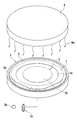
도 2는 척 테이블의 유지면 상에 웨이퍼 및 프레임을 위치시키는 모습을 모식적으로 나타낸 사시도이다.
도 3은 폴리올레핀계 시트 배치 공정을 모식적으로 나타낸 사시도이다.
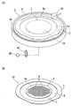
도 4는 일체화 공정의 일례를 모식적으로 나타낸 사시도이다.
도 5는 일체화 공정의 일례를 모식적으로 나타낸 사시도이다.
도 6은 일체화 공정의 일례를 모식적으로 나타낸 사시도이다.
도 7의 (A)는 폴리올레핀계 시트를 절단하는 모습을 모식적으로 나타낸 사시도이고, 도 7의 (B)는 형성된 프레임 유닛을 모식적으로 나타낸 사시도이다.
도 8은 분할 공정을 모식적으로 나타낸 사시도이다.
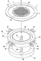
도 9는 픽업 장치로의 프레임 유닛의 반입을 모식적으로 나타낸 사시도이다.
도 10의 (A)는 프레임 지지대 위에 고정된 프레임 유닛을 모식적으로 나타낸 단면도이고, 도 10의 (B)는 픽업 공정을 모식적으로 나타낸 단면도이다.
1b : 이면 3 : 분할 예정 라인
3a : 분할홈 5 : 디바이스
7 : 프레임 7a : 개구
9 : 폴리올레핀계 시트 9a : 절단 자국
11 : 프레임 유닛 2 : 척 테이블
2a : 유지면 2b, 36a : 흡인원
2c, 36b : 전환부 4 : 히트 건
4a : 열풍 6 : 히트 롤러
8 : 적외선 램프 8a : 적외선
10 : 커터 12 : 레이저 가공 장치
14 : 레이저 가공 유닛 14a : 가공 헤드
16 : 레이저빔 18 : 픽업 장치
20 : 드럼 22 : 프레임 유지 유닛
24 : 클램프 26 : 프레임 지지대
28 : 로드 30 : 에어 실린더
32 : 베이스 34 : 푸시업 기구
40 : 콜릿
Claims (7)
- 복수의 디바이스가, 분할 예정 라인에 의해 구획된 표면의 각 영역에 형성된 웨이퍼를 개개의 디바이스 칩으로 분할하는 웨이퍼의 가공 방법으로서,
웨이퍼를 수용하는 개구를 갖는 프레임의 상기 개구 내에 웨이퍼를 위치시키고, 상기 웨이퍼의 이면과 상기 프레임의 외주에 폴리올레핀계 시트를 배치하는 폴리올레핀계 시트 배치 공정과,
상기 폴리올레핀계 시트를 가열하여 열 압착에 의해 상기 웨이퍼와 상기 프레임을 상기 폴리올레핀계 시트를 통해 일체화하는 일체화 공정과,
상기 웨이퍼에 대하여 흡수성을 갖는 파장의 레이저빔을 상기 분할 예정 라인을 따라 상기 웨이퍼에 조사(照射)하고, 분할홈을 형성하여 상기 웨이퍼를 개개의 디바이스 칩으로 분할하는 분할 공정과,
상기 폴리올레핀계 시트로부터 개개의 상기 디바이스 칩을 픽업하는 픽업 공정
을 포함하는 것을 특징으로 하는 웨이퍼의 가공 방법. - 제1항에 있어서, 상기 일체화 공정에 있어서, 적외선의 조사에 의해 상기 열 압착을 실시하는 것을 특징으로 하는 웨이퍼의 가공 방법.
- 제1항에 있어서, 상기 일체화 공정에 있어서, 일체화를 실시한 후, 상기 프레임의 외주로부터 삐져나온 폴리올레핀계 시트를 제거하는 것을 특징으로 하는 웨이퍼의 가공 방법.
- 제1항에 있어서, 상기 픽업 공정에서는, 상기 폴리올레핀계 시트를 확장하여 각 디바이스 칩 사이의 간격을 넓혀, 상기 폴리올레핀계 시트측으로부터 상기 디바이스 칩을 밀어올리는 것을 특징으로 하는 웨이퍼의 가공 방법.
- 제1항에 있어서, 상기 폴리올레핀계 시트는, 폴리에틸렌 시트, 폴리프로필렌 시트, 폴리스티렌 시트 중 어느 하나인 것을 특징으로 하는 웨이퍼의 가공 방법.
- 제5항에 있어서, 상기 일체화 공정에 있어서, 상기 폴리올레핀계 시트가 상기 폴리에틸렌 시트인 경우에 가열 온도는 120℃~140℃이고, 상기 폴리올레핀계 시트가 상기 폴리프로필렌 시트인 경우에 가열 온도는 160℃~180℃이며, 상기 폴리올레핀계 시트가 상기 폴리스티렌 시트인 경우에 가열 온도는 220℃~240℃인 것을 특징으로 하는 웨이퍼의 가공 방법.
- 제1항에 있어서, 상기 웨이퍼는 Si, GaN, GaAs, 유리 중 어느 하나로 구성되는 것을 특징으로 하는 웨이퍼의 가공 방법.
Applications Claiming Priority (2)
| Application Number | Priority Date | Filing Date | Title |
|---|---|---|---|
| JP2018195607A JP7166718B2 (ja) | 2018-10-17 | 2018-10-17 | ウェーハの加工方法 |
| JPJP-P-2018-195607 | 2018-10-17 |
Publications (2)
| Publication Number | Publication Date |
|---|---|
| KR20200043906A true KR20200043906A (ko) | 2020-04-28 |
| KR102752947B1 KR102752947B1 (ko) | 2025-01-10 |
Family
ID=70279764
Family Applications (1)
| Application Number | Title | Priority Date | Filing Date |
|---|---|---|---|
| KR1020190125325A Active KR102752947B1 (ko) | 2018-10-17 | 2019-10-10 | 웨이퍼의 가공 방법 |
Country Status (8)
| Country | Link |
|---|---|
| US (1) | US10720355B2 (ko) |
| JP (1) | JP7166718B2 (ko) |
| KR (1) | KR102752947B1 (ko) |
| CN (1) | CN111063607B (ko) |
| DE (1) | DE102019215999B4 (ko) |
| MY (1) | MY192244A (ko) |
| SG (1) | SG10201909522RA (ko) |
| TW (1) | TWI813794B (ko) |
Families Citing this family (4)
| Publication number | Priority date | Publication date | Assignee | Title |
|---|---|---|---|---|
| JP7430515B2 (ja) * | 2019-11-06 | 2024-02-13 | 株式会社ディスコ | ウエーハの処理方法 |
| US11420173B2 (en) | 2020-03-31 | 2022-08-23 | Yokogawa Electric Corporation | Reaction analysis device, reaction analysis system, and reaction analysis method |
| JP7731231B2 (ja) * | 2021-07-14 | 2025-08-29 | 株式会社ディスコ | 貼着方法及び貼着装置 |
| JP7717582B2 (ja) * | 2021-11-16 | 2025-08-04 | 株式会社ディスコ | ウエーハの加工方法 |
Citations (5)
| Publication number | Priority date | Publication date | Assignee | Title |
|---|---|---|---|---|
| JPH10305420A (ja) | 1997-03-04 | 1998-11-17 | Ngk Insulators Ltd | 酸化物単結晶からなる母材の加工方法、機能性デバイスの製造方法 |
| JP2000138277A (ja) * | 1998-11-02 | 2000-05-16 | Anam Semiconductor Inc | 半導体チップユニットのウェ―ハからのピックアップ方法及びピックアップシステム |
| JP3076179U (ja) | 2000-09-07 | 2001-03-30 | 和雄 落合 | コップ型ボトルキャップ |
| JP2006335860A (ja) * | 2005-06-01 | 2006-12-14 | Lintec Corp | 接着シート |
| JP2012124199A (ja) * | 2010-12-06 | 2012-06-28 | Disco Abrasive Syst Ltd | 板状物の加工方法 |
Family Cites Families (24)
| Publication number | Priority date | Publication date | Assignee | Title |
|---|---|---|---|---|
| JP3076179B2 (ja) | 1993-07-26 | 2000-08-14 | 株式会社ディスコ | ダイシング装置 |
| JP2003152056A (ja) | 2001-11-08 | 2003-05-23 | Sony Corp | 半導体素子保持具及びその製造方法 |
| JP2005191297A (ja) * | 2003-12-25 | 2005-07-14 | Jsr Corp | ダイシングフィルム及び半導体ウェハの切断方法 |
| JP4930679B2 (ja) | 2005-12-14 | 2012-05-16 | 日本ゼオン株式会社 | 半導体素子の製造方法 |
| JP5054933B2 (ja) | 2006-05-23 | 2012-10-24 | ルネサスエレクトロニクス株式会社 | 半導体装置の製造方法 |
| JP4944642B2 (ja) * | 2007-03-09 | 2012-06-06 | 株式会社ディスコ | デバイスの製造方法 |
| JP5307384B2 (ja) * | 2007-12-03 | 2013-10-02 | 株式会社ディスコ | ウエーハの分割方法 |
| JP5047838B2 (ja) | 2008-02-26 | 2012-10-10 | 株式会社ディスコ | テープ貼り機 |
| JP2010027857A (ja) * | 2008-07-18 | 2010-02-04 | Disco Abrasive Syst Ltd | 半導体デバイスの製造方法 |
| JP5432853B2 (ja) * | 2010-07-30 | 2014-03-05 | 日東電工株式会社 | ダイシングテープ一体型半導体裏面用フィルム及びその製造方法並びに半導体装置の製造方法 |
| JP5496167B2 (ja) | 2010-11-12 | 2014-05-21 | 株式会社東京精密 | 半導体ウェハの分割方法及び分割装置 |
| JP5393902B2 (ja) * | 2011-08-09 | 2014-01-22 | 三井化学東セロ株式会社 | 半導体装置の製造方法およびその方法に用いられる半導体ウエハ表面保護用フィルム |
| KR101939636B1 (ko) | 2011-09-30 | 2019-01-17 | 린텍 코포레이션 | 보호막 형성층을 갖는 다이싱 시트 및 칩의 제조 방법 |
| US9230888B2 (en) | 2013-02-11 | 2016-01-05 | Henkel IP & Holding GmbH | Wafer back side coating as dicing tape adhesive |
| JP6425435B2 (ja) | 2014-07-01 | 2018-11-21 | 株式会社ディスコ | チップ間隔維持装置 |
| WO2017002610A1 (ja) * | 2015-06-29 | 2017-01-05 | 三井化学東セロ株式会社 | 半導体部品製造用フィルム |
| KR102042538B1 (ko) * | 2015-11-09 | 2019-11-08 | 후루카와 덴키 고교 가부시키가이샤 | 마스크 일체형 표면 보호 테이프 |
| JP2017152569A (ja) * | 2016-02-25 | 2017-08-31 | 株式会社ディスコ | ウエーハの加工方法 |
| JP2018113281A (ja) * | 2017-01-06 | 2018-07-19 | 株式会社ディスコ | 樹脂パッケージ基板の加工方法 |
| JP6779579B2 (ja) * | 2017-01-31 | 2020-11-04 | 株式会社ディスコ | 判定方法、測定装置、及び粘着テープ貼着装置 |
| SG11201906797WA (en) * | 2017-02-24 | 2019-08-27 | Furukawa Electric Co Ltd | Mask-integrated surface protective tape, and method of producing a semiconductor chip using the same |
| JP6938212B2 (ja) * | 2017-05-11 | 2021-09-22 | 株式会社ディスコ | 加工方法 |
| JP7281873B2 (ja) * | 2018-05-14 | 2023-05-26 | 株式会社ディスコ | ウェーハの加工方法 |
| JP7154686B2 (ja) * | 2018-06-06 | 2022-10-18 | 株式会社ディスコ | ウェーハの加工方法 |
-
2018
- 2018-10-17 JP JP2018195607A patent/JP7166718B2/ja active Active
-
2019
- 2019-09-27 MY MYPI2019005714A patent/MY192244A/en unknown
- 2019-10-10 KR KR1020190125325A patent/KR102752947B1/ko active Active
- 2019-10-10 US US16/598,708 patent/US10720355B2/en active Active
- 2019-10-11 SG SG10201909522RA patent/SG10201909522RA/en unknown
- 2019-10-12 CN CN201910966765.3A patent/CN111063607B/zh active Active
- 2019-10-15 TW TW108137095A patent/TWI813794B/zh active
- 2019-10-17 DE DE102019215999.0A patent/DE102019215999B4/de active Active
Patent Citations (5)
| Publication number | Priority date | Publication date | Assignee | Title |
|---|---|---|---|---|
| JPH10305420A (ja) | 1997-03-04 | 1998-11-17 | Ngk Insulators Ltd | 酸化物単結晶からなる母材の加工方法、機能性デバイスの製造方法 |
| JP2000138277A (ja) * | 1998-11-02 | 2000-05-16 | Anam Semiconductor Inc | 半導体チップユニットのウェ―ハからのピックアップ方法及びピックアップシステム |
| JP3076179U (ja) | 2000-09-07 | 2001-03-30 | 和雄 落合 | コップ型ボトルキャップ |
| JP2006335860A (ja) * | 2005-06-01 | 2006-12-14 | Lintec Corp | 接着シート |
| JP2012124199A (ja) * | 2010-12-06 | 2012-06-28 | Disco Abrasive Syst Ltd | 板状物の加工方法 |
Also Published As
| Publication number | Publication date |
|---|---|
| SG10201909522RA (en) | 2020-05-28 |
| CN111063607B (zh) | 2024-08-27 |
| US10720355B2 (en) | 2020-07-21 |
| TWI813794B (zh) | 2023-09-01 |
| DE102019215999B4 (de) | 2023-06-15 |
| KR102752947B1 (ko) | 2025-01-10 |
| JP2020064956A (ja) | 2020-04-23 |
| MY192244A (en) | 2022-08-10 |
| US20200126859A1 (en) | 2020-04-23 |
| JP7166718B2 (ja) | 2022-11-08 |
| CN111063607A (zh) | 2020-04-24 |
| DE102019215999A1 (de) | 2020-04-23 |
| TW202029318A (zh) | 2020-08-01 |
Similar Documents
| Publication | Publication Date | Title |
|---|---|---|
| KR102777980B1 (ko) | 웨이퍼의 가공 방법 | |
| KR102852746B1 (ko) | 웨이퍼의 가공 방법 | |
| KR20200099979A (ko) | 웨이퍼의 가공 방법 | |
| KR20200070106A (ko) | 웨이퍼의 가공 방법 | |
| KR20200140720A (ko) | 웨이퍼의 가공 방법 | |
| KR102752947B1 (ko) | 웨이퍼의 가공 방법 | |
| KR102702194B1 (ko) | 웨이퍼의 가공 방법 | |
| KR102724205B1 (ko) | 웨이퍼의 가공 방법 | |
| KR20210018072A (ko) | 웨이퍼의 가공 방법 | |
| KR20200052832A (ko) | 웨이퍼의 가공 방법 | |
| KR20200089603A (ko) | 웨이퍼의 가공 방법 | |
| KR102762080B1 (ko) | 웨이퍼의 가공 방법 | |
| KR20200043282A (ko) | 웨이퍼의 가공 방법 | |
| KR20200119726A (ko) | 웨이퍼의 가공 방법 | |
| KR20210031385A (ko) | 웨이퍼의 가공 방법 | |
| KR102772086B1 (ko) | 웨이퍼의 가공 방법 | |
| KR20200130126A (ko) | 웨이퍼의 가공 방법 | |
| KR20200106844A (ko) | 웨이퍼의 가공 방법 | |
| KR20210045934A (ko) | 웨이퍼의 가공 방법 | |
| KR20210007853A (ko) | 웨이퍼의 가공 방법 | |
| KR20200028833A (ko) | 웨이퍼의 가공 방법 | |
| JP7166720B2 (ja) | ウェーハの加工方法 | |
| JP7166719B2 (ja) | ウェーハの加工方法 | |
| KR20210042825A (ko) | 웨이퍼의 가공 방법 | |
| JP2020077683A (ja) | ウェーハの加工方法 |
Legal Events
| Date | Code | Title | Description |
|---|---|---|---|
| PA0109 | Patent application |
St.27 status event code: A-0-1-A10-A12-nap-PA0109 |
|
| PG1501 | Laying open of application |
St.27 status event code: A-1-1-Q10-Q12-nap-PG1501 |
|
| A201 | Request for examination | ||
| PA0201 | Request for examination |
St.27 status event code: A-1-2-D10-D11-exm-PA0201 |
|
| E902 | Notification of reason for refusal | ||
| PE0902 | Notice of grounds for rejection |
St.27 status event code: A-1-2-D10-D21-exm-PE0902 |
|
| P11-X000 | Amendment of application requested |
St.27 status event code: A-2-2-P10-P11-nap-X000 |
|
| P13-X000 | Application amended |
St.27 status event code: A-2-2-P10-P13-nap-X000 |
|
| E701 | Decision to grant or registration of patent right | ||
| PE0701 | Decision of registration |
St.27 status event code: A-1-2-D10-D22-exm-PE0701 |
|
| GRNT | Written decision to grant | ||
| PR0701 | Registration of establishment |
St.27 status event code: A-2-4-F10-F11-exm-PR0701 |
|
| PR1002 | Payment of registration fee |
St.27 status event code: A-2-2-U10-U11-oth-PR1002 Fee payment year number: 1 |
|
| PG1601 | Publication of registration |
St.27 status event code: A-4-4-Q10-Q13-nap-PG1601 |
|
| P22-X000 | Classification modified |
St.27 status event code: A-4-4-P10-P22-nap-X000 |