KR20200045015A - 회로 접속 재료, 회로 접속 구조체, 접착 필름 및 권중체 - Google Patents
회로 접속 재료, 회로 접속 구조체, 접착 필름 및 권중체 Download PDFInfo
- Publication number
- KR20200045015A KR20200045015A KR1020207011815A KR20207011815A KR20200045015A KR 20200045015 A KR20200045015 A KR 20200045015A KR 1020207011815 A KR1020207011815 A KR 1020207011815A KR 20207011815 A KR20207011815 A KR 20207011815A KR 20200045015 A KR20200045015 A KR 20200045015A
- Authority
- KR
- South Korea
- Prior art keywords
- group
- circuit
- film
- adhesive
- mass
- Prior art date
- Legal status (The legal status is an assumption and is not a legal conclusion. Google has not performed a legal analysis and makes no representation as to the accuracy of the status listed.)
- Granted
Links
Images


Classifications
-
- C—CHEMISTRY; METALLURGY
- C09—DYES; PAINTS; POLISHES; NATURAL RESINS; ADHESIVES; COMPOSITIONS NOT OTHERWISE PROVIDED FOR; APPLICATIONS OF MATERIALS NOT OTHERWISE PROVIDED FOR
- C09J—ADHESIVES; NON-MECHANICAL ASPECTS OF ADHESIVE PROCESSES IN GENERAL; ADHESIVE PROCESSES NOT PROVIDED FOR ELSEWHERE; USE OF MATERIALS AS ADHESIVES
- C09J4/00—Adhesives based on organic non-macromolecular compounds having at least one polymerisable carbon-to-carbon unsaturated bond ; adhesives, based on monomers of macromolecular compounds of groups C09J183/00 - C09J183/16
-
- C—CHEMISTRY; METALLURGY
- C09—DYES; PAINTS; POLISHES; NATURAL RESINS; ADHESIVES; COMPOSITIONS NOT OTHERWISE PROVIDED FOR; APPLICATIONS OF MATERIALS NOT OTHERWISE PROVIDED FOR
- C09J—ADHESIVES; NON-MECHANICAL ASPECTS OF ADHESIVE PROCESSES IN GENERAL; ADHESIVE PROCESSES NOT PROVIDED FOR ELSEWHERE; USE OF MATERIALS AS ADHESIVES
- C09J201/00—Adhesives based on unspecified macromolecular compounds
-
- C—CHEMISTRY; METALLURGY
- C09—DYES; PAINTS; POLISHES; NATURAL RESINS; ADHESIVES; COMPOSITIONS NOT OTHERWISE PROVIDED FOR; APPLICATIONS OF MATERIALS NOT OTHERWISE PROVIDED FOR
- C09J—ADHESIVES; NON-MECHANICAL ASPECTS OF ADHESIVE PROCESSES IN GENERAL; ADHESIVE PROCESSES NOT PROVIDED FOR ELSEWHERE; USE OF MATERIALS AS ADHESIVES
- C09J11/00—Features of adhesives not provided for in group C09J9/00, e.g. additives
- C09J11/02—Non-macromolecular additives
- C09J11/04—Non-macromolecular additives inorganic
-
- C—CHEMISTRY; METALLURGY
- C09—DYES; PAINTS; POLISHES; NATURAL RESINS; ADHESIVES; COMPOSITIONS NOT OTHERWISE PROVIDED FOR; APPLICATIONS OF MATERIALS NOT OTHERWISE PROVIDED FOR
- C09J—ADHESIVES; NON-MECHANICAL ASPECTS OF ADHESIVE PROCESSES IN GENERAL; ADHESIVE PROCESSES NOT PROVIDED FOR ELSEWHERE; USE OF MATERIALS AS ADHESIVES
- C09J11/00—Features of adhesives not provided for in group C09J9/00, e.g. additives
- C09J11/02—Non-macromolecular additives
- C09J11/06—Non-macromolecular additives organic
-
- C—CHEMISTRY; METALLURGY
- C09—DYES; PAINTS; POLISHES; NATURAL RESINS; ADHESIVES; COMPOSITIONS NOT OTHERWISE PROVIDED FOR; APPLICATIONS OF MATERIALS NOT OTHERWISE PROVIDED FOR
- C09J—ADHESIVES; NON-MECHANICAL ASPECTS OF ADHESIVE PROCESSES IN GENERAL; ADHESIVE PROCESSES NOT PROVIDED FOR ELSEWHERE; USE OF MATERIALS AS ADHESIVES
- C09J7/00—Adhesives in the form of films or foils
- C09J7/20—Adhesives in the form of films or foils characterised by their carriers
-
- C—CHEMISTRY; METALLURGY
- C09—DYES; PAINTS; POLISHES; NATURAL RESINS; ADHESIVES; COMPOSITIONS NOT OTHERWISE PROVIDED FOR; APPLICATIONS OF MATERIALS NOT OTHERWISE PROVIDED FOR
- C09J—ADHESIVES; NON-MECHANICAL ASPECTS OF ADHESIVE PROCESSES IN GENERAL; ADHESIVE PROCESSES NOT PROVIDED FOR ELSEWHERE; USE OF MATERIALS AS ADHESIVES
- C09J7/00—Adhesives in the form of films or foils
- C09J7/20—Adhesives in the form of films or foils characterised by their carriers
- C09J7/22—Plastics; Metallised plastics
-
- C—CHEMISTRY; METALLURGY
- C09—DYES; PAINTS; POLISHES; NATURAL RESINS; ADHESIVES; COMPOSITIONS NOT OTHERWISE PROVIDED FOR; APPLICATIONS OF MATERIALS NOT OTHERWISE PROVIDED FOR
- C09J—ADHESIVES; NON-MECHANICAL ASPECTS OF ADHESIVE PROCESSES IN GENERAL; ADHESIVE PROCESSES NOT PROVIDED FOR ELSEWHERE; USE OF MATERIALS AS ADHESIVES
- C09J7/00—Adhesives in the form of films or foils
- C09J7/30—Adhesives in the form of films or foils characterised by the adhesive composition
-
- C—CHEMISTRY; METALLURGY
- C09—DYES; PAINTS; POLISHES; NATURAL RESINS; ADHESIVES; COMPOSITIONS NOT OTHERWISE PROVIDED FOR; APPLICATIONS OF MATERIALS NOT OTHERWISE PROVIDED FOR
- C09J—ADHESIVES; NON-MECHANICAL ASPECTS OF ADHESIVE PROCESSES IN GENERAL; ADHESIVE PROCESSES NOT PROVIDED FOR ELSEWHERE; USE OF MATERIALS AS ADHESIVES
- C09J9/00—Adhesives characterised by their physical nature or the effects produced, e.g. glue sticks
- C09J9/02—Electrically-conducting adhesives
-
- H—ELECTRICITY
- H01—ELECTRIC ELEMENTS
- H01R—ELECTRICALLY-CONDUCTIVE CONNECTIONS; STRUCTURAL ASSOCIATIONS OF A PLURALITY OF MUTUALLY-INSULATED ELECTRICAL CONNECTING ELEMENTS; COUPLING DEVICES; CURRENT COLLECTORS
- H01R11/00—Individual connecting elements providing two or more spaced connecting locations for conductive members which are, or may be, thereby interconnected, e.g. end pieces for wires or cables supported by the wire or cable and having means for facilitating electrical connection to some other wire, terminal, or conductive member, blocks of binding posts
- H01R11/01—Individual connecting elements providing two or more spaced connecting locations for conductive members which are, or may be, thereby interconnected, e.g. end pieces for wires or cables supported by the wire or cable and having means for facilitating electrical connection to some other wire, terminal, or conductive member, blocks of binding posts characterised by the form or arrangement of the conductive interconnection between the connecting locations
-
- H—ELECTRICITY
- H05—ELECTRIC TECHNIQUES NOT OTHERWISE PROVIDED FOR
- H05K—PRINTED CIRCUITS; CASINGS OR CONSTRUCTIONAL DETAILS OF ELECTRIC APPARATUS; MANUFACTURE OF ASSEMBLAGES OF ELECTRICAL COMPONENTS
- H05K3/00—Apparatus or processes for manufacturing printed circuits
- H05K3/30—Assembling printed circuits with electric components, e.g. with resistors
- H05K3/32—Assembling printed circuits with electric components, e.g. with resistors electrically connecting electric components or wires to printed circuits
- H05K3/321—Assembling printed circuits with electric components, e.g. with resistors electrically connecting electric components or wires to printed circuits by conductive adhesives
- H05K3/323—Assembling printed circuits with electric components, e.g. with resistors electrically connecting electric components or wires to printed circuits by conductive adhesives by applying an anisotropic conductive adhesive layer over an array of pads
-
- C—CHEMISTRY; METALLURGY
- C08—ORGANIC MACROMOLECULAR COMPOUNDS; THEIR PREPARATION OR CHEMICAL WORKING-UP; COMPOSITIONS BASED THEREON
- C08K—Use of inorganic or non-macromolecular organic substances as compounding ingredients
- C08K2201/00—Specific properties of additives
- C08K2201/001—Conductive additives
-
- C—CHEMISTRY; METALLURGY
- C08—ORGANIC MACROMOLECULAR COMPOUNDS; THEIR PREPARATION OR CHEMICAL WORKING-UP; COMPOSITIONS BASED THEREON
- C08K—Use of inorganic or non-macromolecular organic substances as compounding ingredients
- C08K3/00—Use of inorganic substances as compounding ingredients
- C08K3/18—Oxygen-containing compounds, e.g. metal carbonyls
- C08K3/20—Oxides; Hydroxides
- C08K3/22—Oxides; Hydroxides of metals
-
- C—CHEMISTRY; METALLURGY
- C08—ORGANIC MACROMOLECULAR COMPOUNDS; THEIR PREPARATION OR CHEMICAL WORKING-UP; COMPOSITIONS BASED THEREON
- C08K—Use of inorganic or non-macromolecular organic substances as compounding ingredients
- C08K5/00—Use of organic ingredients
- C08K5/54—Silicon-containing compounds
-
- C—CHEMISTRY; METALLURGY
- C09—DYES; PAINTS; POLISHES; NATURAL RESINS; ADHESIVES; COMPOSITIONS NOT OTHERWISE PROVIDED FOR; APPLICATIONS OF MATERIALS NOT OTHERWISE PROVIDED FOR
- C09J—ADHESIVES; NON-MECHANICAL ASPECTS OF ADHESIVE PROCESSES IN GENERAL; ADHESIVE PROCESSES NOT PROVIDED FOR ELSEWHERE; USE OF MATERIALS AS ADHESIVES
- C09J2301/00—Additional features of adhesives in the form of films or foils
- C09J2301/30—Additional features of adhesives in the form of films or foils characterized by the chemical, physicochemical or physical properties of the adhesive or the carrier
- C09J2301/314—Additional features of adhesives in the form of films or foils characterized by the chemical, physicochemical or physical properties of the adhesive or the carrier the adhesive layer and/or the carrier being conductive
-
- C—CHEMISTRY; METALLURGY
- C09—DYES; PAINTS; POLISHES; NATURAL RESINS; ADHESIVES; COMPOSITIONS NOT OTHERWISE PROVIDED FOR; APPLICATIONS OF MATERIALS NOT OTHERWISE PROVIDED FOR
- C09J—ADHESIVES; NON-MECHANICAL ASPECTS OF ADHESIVE PROCESSES IN GENERAL; ADHESIVE PROCESSES NOT PROVIDED FOR ELSEWHERE; USE OF MATERIALS AS ADHESIVES
- C09J2301/00—Additional features of adhesives in the form of films or foils
- C09J2301/40—Additional features of adhesives in the form of films or foils characterized by the presence of essential components
- C09J2301/408—Additional features of adhesives in the form of films or foils characterized by the presence of essential components additives as essential feature of the adhesive layer
-
- H—ELECTRICITY
- H01—ELECTRIC ELEMENTS
- H01R—ELECTRICALLY-CONDUCTIVE CONNECTIONS; STRUCTURAL ASSOCIATIONS OF A PLURALITY OF MUTUALLY-INSULATED ELECTRICAL CONNECTING ELEMENTS; COUPLING DEVICES; CURRENT COLLECTORS
- H01R12/00—Structural associations of a plurality of mutually-insulated electrical connecting elements, specially adapted for printed circuits, e.g. printed circuit boards [PCB], flat or ribbon cables, or like generally planar structures, e.g. terminal strips, terminal blocks; Coupling devices specially adapted for printed circuits, flat or ribbon cables, or like generally planar structures; Terminals specially adapted for contact with, or insertion into, printed circuits, flat or ribbon cables, or like generally planar structures
- H01R12/50—Fixed connections
- H01R12/51—Fixed connections for rigid printed circuits or like structures
- H01R12/52—Fixed connections for rigid printed circuits or like structures connecting to other rigid printed circuits or like structures
-
- H—ELECTRICITY
- H01—ELECTRIC ELEMENTS
- H01R—ELECTRICALLY-CONDUCTIVE CONNECTIONS; STRUCTURAL ASSOCIATIONS OF A PLURALITY OF MUTUALLY-INSULATED ELECTRICAL CONNECTING ELEMENTS; COUPLING DEVICES; CURRENT COLLECTORS
- H01R4/00—Electrically-conductive connections between two or more conductive members in direct contact, i.e. touching one another; Means for effecting or maintaining such contact; Electrically-conductive connections having two or more spaced connecting locations for conductors and using contact members penetrating insulation
- H01R4/04—Electrically-conductive connections between two or more conductive members in direct contact, i.e. touching one another; Means for effecting or maintaining such contact; Electrically-conductive connections having two or more spaced connecting locations for conductors and using contact members penetrating insulation using electrically conductive adhesives
-
- H—ELECTRICITY
- H05—ELECTRIC TECHNIQUES NOT OTHERWISE PROVIDED FOR
- H05K—PRINTED CIRCUITS; CASINGS OR CONSTRUCTIONAL DETAILS OF ELECTRIC APPARATUS; MANUFACTURE OF ASSEMBLAGES OF ELECTRICAL COMPONENTS
- H05K2201/00—Indexing scheme relating to printed circuits covered by H05K1/00
- H05K2201/01—Dielectrics
- H05K2201/0104—Properties and characteristics in general
- H05K2201/0129—Thermoplastic polymer, e.g. auto-adhesive layer; Shaping of thermoplastic polymer
-
- H—ELECTRICITY
- H05—ELECTRIC TECHNIQUES NOT OTHERWISE PROVIDED FOR
- H05K—PRINTED CIRCUITS; CASINGS OR CONSTRUCTIONAL DETAILS OF ELECTRIC APPARATUS; MANUFACTURE OF ASSEMBLAGES OF ELECTRICAL COMPONENTS
- H05K3/00—Apparatus or processes for manufacturing printed circuits
- H05K3/36—Assembling printed circuits with other printed circuits
- H05K3/361—Assembling flexible printed circuits with other printed circuits
-
- H—ELECTRICITY
- H10—SEMICONDUCTOR DEVICES; ELECTRIC SOLID-STATE DEVICES NOT OTHERWISE PROVIDED FOR
- H10W—GENERIC PACKAGES, INTERCONNECTIONS, CONNECTORS OR OTHER CONSTRUCTIONAL DETAILS OF DEVICES COVERED BY CLASS H10
- H10W72/00—Interconnections or connectors in packages
- H10W72/01—Manufacture or treatment
- H10W72/013—Manufacture or treatment of die-attach connectors
- H10W72/01331—Manufacture or treatment of die-attach connectors using blanket deposition
- H10W72/01336—Manufacture or treatment of die-attach connectors using blanket deposition in solid form, e.g. by using a powder or by laminating a foil
-
- H—ELECTRICITY
- H10—SEMICONDUCTOR DEVICES; ELECTRIC SOLID-STATE DEVICES NOT OTHERWISE PROVIDED FOR
- H10W—GENERIC PACKAGES, INTERCONNECTIONS, CONNECTORS OR OTHER CONSTRUCTIONAL DETAILS OF DEVICES COVERED BY CLASS H10
- H10W72/00—Interconnections or connectors in packages
- H10W72/071—Connecting or disconnecting
- H10W72/073—Connecting or disconnecting of die-attach connectors
- H10W72/07331—Connecting techniques
- H10W72/07332—Compression bonding, e.g. thermocompression bonding
-
- H—ELECTRICITY
- H10—SEMICONDUCTOR DEVICES; ELECTRIC SOLID-STATE DEVICES NOT OTHERWISE PROVIDED FOR
- H10W—GENERIC PACKAGES, INTERCONNECTIONS, CONNECTORS OR OTHER CONSTRUCTIONAL DETAILS OF DEVICES COVERED BY CLASS H10
- H10W72/00—Interconnections or connectors in packages
- H10W72/071—Connecting or disconnecting
- H10W72/073—Connecting or disconnecting of die-attach connectors
- H10W72/07331—Connecting techniques
- H10W72/07336—Soldering or alloying
-
- H—ELECTRICITY
- H10—SEMICONDUCTOR DEVICES; ELECTRIC SOLID-STATE DEVICES NOT OTHERWISE PROVIDED FOR
- H10W—GENERIC PACKAGES, INTERCONNECTIONS, CONNECTORS OR OTHER CONSTRUCTIONAL DETAILS OF DEVICES COVERED BY CLASS H10
- H10W72/00—Interconnections or connectors in packages
- H10W72/071—Connecting or disconnecting
- H10W72/074—Connecting or disconnecting of anisotropic conductive adhesives
-
- H—ELECTRICITY
- H10—SEMICONDUCTOR DEVICES; ELECTRIC SOLID-STATE DEVICES NOT OTHERWISE PROVIDED FOR
- H10W—GENERIC PACKAGES, INTERCONNECTIONS, CONNECTORS OR OTHER CONSTRUCTIONAL DETAILS OF DEVICES COVERED BY CLASS H10
- H10W72/00—Interconnections or connectors in packages
- H10W72/20—Bump connectors, e.g. solder bumps or copper pillars; Dummy bumps; Thermal bumps
- H10W72/261—Functions other than electrical connecting
-
- H—ELECTRICITY
- H10—SEMICONDUCTOR DEVICES; ELECTRIC SOLID-STATE DEVICES NOT OTHERWISE PROVIDED FOR
- H10W—GENERIC PACKAGES, INTERCONNECTIONS, CONNECTORS OR OTHER CONSTRUCTIONAL DETAILS OF DEVICES COVERED BY CLASS H10
- H10W72/00—Interconnections or connectors in packages
- H10W72/30—Die-attach connectors
- H10W72/321—Structures or relative sizes of die-attach connectors
- H10W72/325—Die-attach connectors having a filler embedded in a matrix
-
- H—ELECTRICITY
- H10—SEMICONDUCTOR DEVICES; ELECTRIC SOLID-STATE DEVICES NOT OTHERWISE PROVIDED FOR
- H10W—GENERIC PACKAGES, INTERCONNECTIONS, CONNECTORS OR OTHER CONSTRUCTIONAL DETAILS OF DEVICES COVERED BY CLASS H10
- H10W72/00—Interconnections or connectors in packages
- H10W72/30—Die-attach connectors
- H10W72/351—Materials of die-attach connectors
- H10W72/352—Materials of die-attach connectors comprising metals or metalloids, e.g. solders
-
- H—ELECTRICITY
- H10—SEMICONDUCTOR DEVICES; ELECTRIC SOLID-STATE DEVICES NOT OTHERWISE PROVIDED FOR
- H10W—GENERIC PACKAGES, INTERCONNECTIONS, CONNECTORS OR OTHER CONSTRUCTIONAL DETAILS OF DEVICES COVERED BY CLASS H10
- H10W72/00—Interconnections or connectors in packages
- H10W72/30—Die-attach connectors
- H10W72/351—Materials of die-attach connectors
- H10W72/353—Materials of die-attach connectors not comprising solid metals or solid metalloids, e.g. ceramics
- H10W72/354—Materials of die-attach connectors not comprising solid metals or solid metalloids, e.g. ceramics comprising polymers
-
- H—ELECTRICITY
- H10—SEMICONDUCTOR DEVICES; ELECTRIC SOLID-STATE DEVICES NOT OTHERWISE PROVIDED FOR
- H10W—GENERIC PACKAGES, INTERCONNECTIONS, CONNECTORS OR OTHER CONSTRUCTIONAL DETAILS OF DEVICES COVERED BY CLASS H10
- H10W90/00—Package configurations
- H10W90/701—Package configurations characterised by the relative positions of pads or connectors relative to package parts
- H10W90/731—Package configurations characterised by the relative positions of pads or connectors relative to package parts of die-attach connectors
- H10W90/734—Package configurations characterised by the relative positions of pads or connectors relative to package parts of die-attach connectors between a chip and a stacked insulating package substrate, interposer or RDL
-
- H—ELECTRICITY
- H10—SEMICONDUCTOR DEVICES; ELECTRIC SOLID-STATE DEVICES NOT OTHERWISE PROVIDED FOR
- H10W—GENERIC PACKAGES, INTERCONNECTIONS, CONNECTORS OR OTHER CONSTRUCTIONAL DETAILS OF DEVICES COVERED BY CLASS H10
- H10W99/00—Subject matter not provided for in other groups of this subclass
-
- Y—GENERAL TAGGING OF NEW TECHNOLOGICAL DEVELOPMENTS; GENERAL TAGGING OF CROSS-SECTIONAL TECHNOLOGIES SPANNING OVER SEVERAL SECTIONS OF THE IPC; TECHNICAL SUBJECTS COVERED BY FORMER USPC CROSS-REFERENCE ART COLLECTIONS [XRACs] AND DIGESTS
- Y10—TECHNICAL SUBJECTS COVERED BY FORMER USPC
- Y10S—TECHNICAL SUBJECTS COVERED BY FORMER USPC CROSS-REFERENCE ART COLLECTIONS [XRACs] AND DIGESTS
- Y10S428/00—Stock material or miscellaneous articles
- Y10S428/913—Material designed to be responsive to temperature, light, moisture
Landscapes
- Chemical & Material Sciences (AREA)
- Organic Chemistry (AREA)
- Inorganic Chemistry (AREA)
- Engineering & Computer Science (AREA)
- Manufacturing & Machinery (AREA)
- Microelectronics & Electronic Packaging (AREA)
- Adhesives Or Adhesive Processes (AREA)
- Adhesive Tapes (AREA)
- Structures Or Materials For Encapsulating Or Coating Semiconductor Devices Or Solid State Devices (AREA)
- Wire Bonding (AREA)
- Conductive Materials (AREA)
Abstract
<화학식 1>

Description

도 2는 본 발명의 접속 구조체의 일 실시 형태를 도시하는 모식 단면도이다.
도 3의 (a) 내지 (c)는 회로 부재를 접속하는 일련의 공정을 도시하는 공정도이다.





5: 회로 접속 재료
7: 도전성 입자
10: 접속 부재
11: 절연성 물질
20: 제1 회로 부재
21: 회로 기판(제1 회로 기판)
21a: 주면
22: 회로 전극(제1 회로 전극)
30: 제2 회로 부재
31: 회로 기판(제2 회로 기판)
31a: 주면
32: 회로 전극(제2 회로 전극)
40: 필름상 접착제
Claims (1)
- 열 가소성 수지, 라디칼 중합성 화합물, 라디칼 중합 개시제 및 무기 미립자를 함유하는 조성물의, 서로 대향하는 2개의 회로 부재를 전기적으로 접속하기 위한 회로 접속 재료로서의 용도로서,
상기 라디칼 중합성 화합물의 함유량이 상기 조성물의 전량 기준으로 40질량% 이상이고,
상기 라디칼 중합성 화합물 중 분자량 1000 이하의 화합물의 함유량이 상기 조성물의 전량 기준으로 15질량% 이하이고,
상기 무기 미립자의 함유량이 상기 조성물의 전량 기준으로 5 내지 30질량%이고,
상기 조성물이 적어도 하기 화학식 1로 표시되는 화합물을 함유하는, 용도.
<화학식 1>
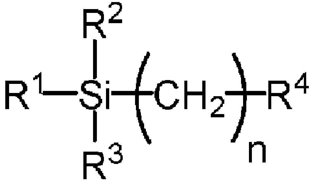
[식 중, R1, R2 및 R3은 각각 독립적으로 수소 원자, 탄소수 1 내지 5의 알킬기, 탄소수 1 내지 5의 알콕시기, 탄소수 1 내지 5의 알콕시카르보닐기 또는 아릴기를 나타내며, R1, R2 및 R3 중 적어도 하나는 탄소수 1 내지 5의 알콕시기이고, R4는 (메트)아크릴로일기, 비닐기, 이소시아네이트기, 이미다졸기, 머캅토기, 아미노기, 메틸아미노기, 디메틸아미노기, 벤질아미노기, 페닐아미노기, 시클로헥실아미노기, 모르폴리노기, 피페라지노기, 우레이도기 또는 글리시딜기를 나타내고, n은 1 내지 10의 정수를 나타냄]
Applications Claiming Priority (4)
| Application Number | Priority Date | Filing Date | Title |
|---|---|---|---|
| JPJP-P-2012-100207 | 2012-04-25 | ||
| JP2012100207 | 2012-04-25 | ||
| KR1020147024907A KR20150005516A (ko) | 2012-04-25 | 2013-04-19 | 회로 접속 재료, 회로 접속 구조체, 접착 필름 및 권중체 |
| PCT/JP2013/061658 WO2013161713A1 (ja) | 2012-04-25 | 2013-04-19 | 回路接続材料、回路接続構造体、接着フィルム及び巻重体 |
Related Parent Applications (1)
| Application Number | Title | Priority Date | Filing Date |
|---|---|---|---|
| KR1020147024907A Division KR20150005516A (ko) | 2012-04-25 | 2013-04-19 | 회로 접속 재료, 회로 접속 구조체, 접착 필름 및 권중체 |
Publications (2)
| Publication Number | Publication Date |
|---|---|
| KR20200045015A true KR20200045015A (ko) | 2020-04-29 |
| KR102329065B1 KR102329065B1 (ko) | 2021-11-18 |
Family
ID=49483032
Family Applications (2)
| Application Number | Title | Priority Date | Filing Date |
|---|---|---|---|
| KR1020147024907A Ceased KR20150005516A (ko) | 2012-04-25 | 2013-04-19 | 회로 접속 재료, 회로 접속 구조체, 접착 필름 및 권중체 |
| KR1020207011815A Active KR102329065B1 (ko) | 2012-04-25 | 2013-04-19 | 회로 접속 재료, 회로 접속 구조체, 접착 필름 및 권중체 |
Family Applications Before (1)
| Application Number | Title | Priority Date | Filing Date |
|---|---|---|---|
| KR1020147024907A Ceased KR20150005516A (ko) | 2012-04-25 | 2013-04-19 | 회로 접속 재료, 회로 접속 구조체, 접착 필름 및 권중체 |
Country Status (4)
| Country | Link |
|---|---|
| JP (1) | JP6090311B2 (ko) |
| KR (2) | KR20150005516A (ko) |
| CN (1) | CN104169389B (ko) |
| WO (1) | WO2013161713A1 (ko) |
Families Citing this family (13)
| Publication number | Priority date | Publication date | Assignee | Title |
|---|---|---|---|---|
| JP6492628B2 (ja) * | 2014-12-22 | 2019-04-03 | 日立化成株式会社 | アンダーフィル材、電子部品装置の製造方法及び電子部品装置 |
| JP6148267B2 (ja) * | 2015-02-18 | 2017-06-14 | 株式会社タムラ製作所 | 異方性導電性ペーストおよびそれを用いたプリント配線基板の製造方法 |
| JPWO2016143640A1 (ja) * | 2015-03-11 | 2017-12-28 | セメダイン株式会社 | 導電性構造体、及び導電性構造体の製造方法 |
| CN104952702B (zh) * | 2015-05-15 | 2017-11-28 | 张家港康得新光电材料有限公司 | 半导体器件及其制作方法 |
| WO2016199252A1 (ja) * | 2015-06-10 | 2016-12-15 | 日立化成株式会社 | 接着剤組成物及び接続体 |
| TWI685554B (zh) * | 2015-06-16 | 2020-02-21 | 日商日立化成股份有限公司 | 接著劑組成物及連接體 |
| WO2017078087A1 (ja) * | 2015-11-04 | 2017-05-11 | 日立化成株式会社 | 接着剤組成物及び構造体 |
| JP6958359B2 (ja) * | 2015-11-25 | 2021-11-02 | 昭和電工マテリアルズ株式会社 | 接着剤組成物及び構造体 |
| JP2017103303A (ja) * | 2015-11-30 | 2017-06-08 | 日立化成株式会社 | 半導体用接着剤、半導体装置、及び半導体装置の製造方法 |
| CN106549115B (zh) * | 2016-10-27 | 2018-07-20 | 武汉华星光电技术有限公司 | 异方性导电胶膜及异方性导电胶膜的剥离方法 |
| JP7279639B2 (ja) * | 2017-11-08 | 2023-05-23 | 株式会社レゾナック | 接合体の製造方法及び接合材 |
| WO2022186016A1 (ja) * | 2021-03-01 | 2022-09-09 | 昭和電工マテリアルズ株式会社 | 回路接続用接着フィルム及び接続体 |
| CN114927256A (zh) * | 2022-04-29 | 2022-08-19 | 常州德创高新材料科技有限公司 | 一种电路连接材料 |
Citations (4)
| Publication number | Priority date | Publication date | Assignee | Title |
|---|---|---|---|---|
| JPH01113480A (ja) | 1987-10-27 | 1989-05-02 | Sony Chem Corp | 熱硬化型異方性導電接着剤 |
| JPH08325543A (ja) * | 1995-06-05 | 1996-12-10 | Soken Chem & Eng Co Ltd | 異方導電性接着剤 |
| JP2009110913A (ja) * | 2007-10-30 | 2009-05-21 | Cheil Industries Inc | 半熱硬化性異方導電性フィルム組成物 |
| US9844067B2 (en) | 2013-07-11 | 2017-12-12 | Lg Electronics Inc. | Broadcasting method using device-to-device (D2D) communication in wireless communication system |
Family Cites Families (10)
| Publication number | Priority date | Publication date | Assignee | Title |
|---|---|---|---|---|
| JP3871095B2 (ja) * | 1998-03-31 | 2007-01-24 | 日立化成工業株式会社 | 回路板装置の製造法 |
| JP2001126541A (ja) * | 1999-10-28 | 2001-05-11 | Sumitomo Bakelite Co Ltd | 異方導電フィルム及び電気・電子部品 |
| JP2004067908A (ja) * | 2002-08-07 | 2004-03-04 | Sumitomo Bakelite Co Ltd | 異方導電性接着剤 |
| JP4760070B2 (ja) * | 2005-03-16 | 2011-08-31 | 日立化成工業株式会社 | 接着剤、回路接続用接着剤、接続体及び半導体装置 |
| WO2008023670A1 (fr) * | 2006-08-22 | 2008-02-28 | Hitachi Chemical Company, Ltd. | matériau de connexion de circuits, structure de connexion d'un élément de circuit et procédés de fabrication de ladite structure |
| KR100902714B1 (ko) * | 2006-12-29 | 2009-06-15 | 제일모직주식회사 | 반열경화성 이방 도전성 필름 조성물 |
| KR101240009B1 (ko) * | 2007-09-19 | 2013-03-06 | 히타치가세이가부시끼가이샤 | 접착제 조성물 및 접합체 |
| JP4985700B2 (ja) * | 2008-04-28 | 2012-07-25 | 日立化成工業株式会社 | 接着剤リール |
| JP5577635B2 (ja) * | 2008-10-09 | 2014-08-27 | 日立化成株式会社 | 接着剤組成物、回路接続用接着剤及び回路接続体 |
| JP5293779B2 (ja) * | 2010-07-20 | 2013-09-18 | 日立化成株式会社 | 接着剤組成物、回路接続構造体、半導体装置及び太陽電池モジュール |
-
2013
- 2013-04-19 KR KR1020147024907A patent/KR20150005516A/ko not_active Ceased
- 2013-04-19 KR KR1020207011815A patent/KR102329065B1/ko active Active
- 2013-04-19 WO PCT/JP2013/061658 patent/WO2013161713A1/ja not_active Ceased
- 2013-04-19 JP JP2014512528A patent/JP6090311B2/ja active Active
- 2013-04-19 CN CN201380014782.8A patent/CN104169389B/zh active Active
Patent Citations (4)
| Publication number | Priority date | Publication date | Assignee | Title |
|---|---|---|---|---|
| JPH01113480A (ja) | 1987-10-27 | 1989-05-02 | Sony Chem Corp | 熱硬化型異方性導電接着剤 |
| JPH08325543A (ja) * | 1995-06-05 | 1996-12-10 | Soken Chem & Eng Co Ltd | 異方導電性接着剤 |
| JP2009110913A (ja) * | 2007-10-30 | 2009-05-21 | Cheil Industries Inc | 半熱硬化性異方導電性フィルム組成物 |
| US9844067B2 (en) | 2013-07-11 | 2017-12-12 | Lg Electronics Inc. | Broadcasting method using device-to-device (D2D) communication in wireless communication system |
Also Published As
| Publication number | Publication date |
|---|---|
| KR20150005516A (ko) | 2015-01-14 |
| CN104169389A (zh) | 2014-11-26 |
| CN104169389B (zh) | 2018-07-13 |
| KR102329065B1 (ko) | 2021-11-18 |
| WO2013161713A1 (ja) | 2013-10-31 |
| JPWO2013161713A1 (ja) | 2015-12-24 |
| JP6090311B2 (ja) | 2017-03-08 |
Similar Documents
| Publication | Publication Date | Title |
|---|---|---|
| KR102329065B1 (ko) | 회로 접속 재료, 회로 접속 구조체, 접착 필름 및 권중체 | |
| JP4998468B2 (ja) | 接着剤組成物及び回路部材の接続構造 | |
| JP5223679B2 (ja) | 接着剤及びこれを用いた接続構造体 | |
| KR102478959B1 (ko) | 접착제 조성물 및 접속체 | |
| JP6173928B2 (ja) | 接着剤組成物、回路接続用接着剤及び接続体 | |
| JP4760070B2 (ja) | 接着剤、回路接続用接着剤、接続体及び半導体装置 | |
| JP5251393B2 (ja) | 接着剤組成物、回路接続用接着剤及びそれを用いた接続体 | |
| JP5292838B2 (ja) | 接着剤、及び回路部材の接続構造体 | |
| KR101379152B1 (ko) | 접착제 조성물, 회로 접속 구조체, 반도체 장치 및 태양 전지 모듈 | |
| JP6307966B2 (ja) | 接着剤組成物、異方導電性接着剤組成物、回路接続材料及び接続体 | |
| JP5560544B2 (ja) | 接着剤組成物、フィルム状接着剤、回路接続用接着剤、接続体及び半導体装置 | |
| JP5577635B2 (ja) | 接着剤組成物、回路接続用接着剤及び回路接続体 | |
| JP2009256581A (ja) | 接着剤組成物、回路接続用接着剤及びそれを用いた接続体 | |
| JP2013227420A (ja) | 回路接続材料、回路接続構造体、接着フィルム及び巻重体。 | |
| JP2012204059A (ja) | 回路接続材料及びそれを用いた回路接続構造体 | |
| JP6631631B2 (ja) | 接着剤組成物、異方導電性接着剤組成物、回路接続材料及び接続体 | |
| KR102397238B1 (ko) | 접착제 조성물 및 접속체 | |
| JP2011157557A (ja) | 接着剤、回路接続用接着剤、接続体及び半導体装置 |
Legal Events
| Date | Code | Title | Description |
|---|---|---|---|
| A107 | Divisional application of patent | ||
| PA0104 | Divisional application for international application |
Comment text: Divisional Application for International Patent Patent event code: PA01041R01D Patent event date: 20200423 Application number text: 1020147024907 Filing date: 20140904 |
|
| PG1501 | Laying open of application | ||
| A201 | Request for examination | ||
| PA0201 | Request for examination |
Patent event code: PA02012R01D Patent event date: 20200522 Comment text: Request for Examination of Application |
|
| E902 | Notification of reason for refusal | ||
| PE0902 | Notice of grounds for rejection |
Comment text: Notification of reason for refusal Patent event date: 20200730 Patent event code: PE09021S01D |
|
| E701 | Decision to grant or registration of patent right | ||
| PE0701 | Decision of registration |
Patent event code: PE07011S01D Comment text: Decision to Grant Registration Patent event date: 20210820 |
|
| GRNT | Written decision to grant | ||
| PR0701 | Registration of establishment |
Comment text: Registration of Establishment Patent event date: 20211116 Patent event code: PR07011E01D |
|
| PR1002 | Payment of registration fee |
Payment date: 20211116 End annual number: 3 Start annual number: 1 |
|
| PG1601 | Publication of registration |