KR20200055258A - 테이프를 대신하는 박막필름의 형성 방법 - Google Patents
테이프를 대신하는 박막필름의 형성 방법 Download PDFInfo
- Publication number
- KR20200055258A KR20200055258A KR1020180138668A KR20180138668A KR20200055258A KR 20200055258 A KR20200055258 A KR 20200055258A KR 1020180138668 A KR1020180138668 A KR 1020180138668A KR 20180138668 A KR20180138668 A KR 20180138668A KR 20200055258 A KR20200055258 A KR 20200055258A
- Authority
- KR
- South Korea
- Prior art keywords
- thin film
- liquid material
- substrate
- curing
- tape
- Prior art date
- Legal status (The legal status is an assumption and is not a legal conclusion. Google has not performed a legal analysis and makes no representation as to the accuracy of the status listed.)
- Granted
Links
Images


Classifications
-
- H—ELECTRICITY
- H10—SEMICONDUCTOR DEVICES; ELECTRIC SOLID-STATE DEVICES NOT OTHERWISE PROVIDED FOR
- H10P—GENERIC PROCESSES OR APPARATUS FOR THE MANUFACTURE OR TREATMENT OF DEVICES COVERED BY CLASS H10
- H10P72/00—Handling or holding of wafers, substrates or devices during manufacture or treatment thereof
- H10P72/04—Apparatus for manufacture or treatment
- H10P72/0442—Apparatus for placing on an insulating substrate, e.g. tape
-
- H01L21/67132—
-
- H01L21/02016—
-
- H01L21/02307—
-
- H01L21/6836—
-
- H01L21/78—
-
- H—ELECTRICITY
- H10—SEMICONDUCTOR DEVICES; ELECTRIC SOLID-STATE DEVICES NOT OTHERWISE PROVIDED FOR
- H10P—GENERIC PROCESSES OR APPARATUS FOR THE MANUFACTURE OR TREATMENT OF DEVICES COVERED BY CLASS H10
- H10P14/00—Formation of materials, e.g. in the shape of layers or pillars
- H10P14/60—Formation of materials, e.g. in the shape of layers or pillars of insulating materials
- H10P14/65—Formation of materials, e.g. in the shape of layers or pillars of insulating materials characterised by treatments performed before or after the formation of the materials
- H10P14/6502—Formation of materials, e.g. in the shape of layers or pillars of insulating materials characterised by treatments performed before or after the formation of the materials of treatments performed before formation of the materials
- H10P14/6508—Formation of materials, e.g. in the shape of layers or pillars of insulating materials characterised by treatments performed before or after the formation of the materials of treatments performed before formation of the materials by exposure to a liquid
-
- H—ELECTRICITY
- H10—SEMICONDUCTOR DEVICES; ELECTRIC SOLID-STATE DEVICES NOT OTHERWISE PROVIDED FOR
- H10P—GENERIC PROCESSES OR APPARATUS FOR THE MANUFACTURE OR TREATMENT OF DEVICES COVERED BY CLASS H10
- H10P54/00—Cutting or separating of wafers, substrates or parts of devices
-
- H—ELECTRICITY
- H10—SEMICONDUCTOR DEVICES; ELECTRIC SOLID-STATE DEVICES NOT OTHERWISE PROVIDED FOR
- H10P—GENERIC PROCESSES OR APPARATUS FOR THE MANUFACTURE OR TREATMENT OF DEVICES COVERED BY CLASS H10
- H10P72/00—Handling or holding of wafers, substrates or devices during manufacture or treatment thereof
- H10P72/70—Handling or holding of wafers, substrates or devices during manufacture or treatment thereof for supporting or gripping
- H10P72/74—Handling or holding of wafers, substrates or devices during manufacture or treatment thereof for supporting or gripping using temporarily an auxiliary support
- H10P72/7402—Wafer tapes, e.g. grinding or dicing support tapes
-
- H—ELECTRICITY
- H10—SEMICONDUCTOR DEVICES; ELECTRIC SOLID-STATE DEVICES NOT OTHERWISE PROVIDED FOR
- H10P—GENERIC PROCESSES OR APPARATUS FOR THE MANUFACTURE OR TREATMENT OF DEVICES COVERED BY CLASS H10
- H10P90/00—Preparation of wafers not covered by a single main group of this subclass, e.g. wafer reinforcement
- H10P90/12—Preparing bulk and homogeneous wafers
- H10P90/124—Preparing bulk and homogeneous wafers by processing the backside of the wafers
Landscapes
- Mechanical Treatment Of Semiconductor (AREA)
- Application Of Or Painting With Fluid Materials (AREA)
Abstract
Description
도 2는 예시적인 실시예들에 따른 테이프를 대신하는 박막필름을 형성하지 않은 기판의 상태를 나타내는 사진이고, 도 3은 예시적인 실시예들에 따른 테이프를 대신하는 박막필름을 형성한 기판의 상태를 나타내는 사진이다.
도 4는 예시적인 실시예들에 따른 테이프를 대신하는 박막필름을 형성하지 않은 기판의 상태를 설명하기 위한 도면이고, 도 5 및 도 6은 예시적인 실시예들에 따른 테이프를 대신하는 박막필름을 형성한 기판의 상태를 설명하기 위한 도면들이다.
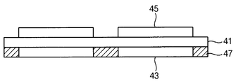
43, 45 : 이엠씨
47 : 박막필름
Claims (10)
- 기판 상에 모노머 구조를 갖는 액상 물질을 도포하는 단계;
상기 기판 상에 도포되는 모노머 구조를 갖는 액상 물질이 올리고머 구조를 갖는 예비 박막필름으로 형성되도록 상기 액상 물질을 경화시키는 단계; 및
상기 올리고머 구조를 갖는 예비 박막필름이 폴리머 구조를 갖는 박막필름으로 형성되도록 상기 예비 박막필름을 경화시키는 단계를 포함하는 것을 특징으로 하는 테이프를 대신하는 박막필름의 형성 방법. - 제1 항에 있어서,
상기 올리고머 구조를 갖는 예비 박막필름이 설정 두께를 가질 때까지 상기 액상 물질의 도포 및 상기 액상 물질의 경화를 계속적으로 수행하는 단계를 더 포함하는 것을 특징으로 하는 테이프를 대신하는 박막필름의 형성 방법. - 제1 항에 있어서,
상기 액상 물질은 압전 소자로부터 인가되는 전기적 제어에 의해 상기 액상 물질의 도포량이 조절되는 노즐들을 구비하는 프린터 헤드를 사용하여 상기 기판 상에 도포하는 것을 특징으로 하는 테이프를 대신하는 박막필름의 형성 방법. - 제1 항에 있어서,
상기 액상 물질의 경화 및 상기 예비 박막필름의 경화는 300 내지 450nm의 파장을 갖는 자외선을 방출할 수 있는 UV-LED를 사용하는 것을 특징으로 하는 테이프를 대신하는 박막필름의 형성 방법. - 제1 항에 있어서,
상기 액상 물질의 도포, 상기 액상 물질의 경화 및 상기 예비 박막필름의 경화는 상기 기판을 고정시킨 상태에서 상기 액상 물질을 도포할 수 있는 프린터 헤드와, 상기 액상 물질 및 상기 예비 박막필름을 경화시킬 수 있는 UV-LED를 이동시키면서 수행하는 것을 특징으로 하는 테이프를 대신하는 박막필름의 형성 방법. - 제1 항에 있어서,
상기 액상 물질의 도포, 상기 액상 물질의 경화 및 상기 예비 박막필름의 경화는 상기 액상 물질을 도포할 수 있는 프린터 헤드와, 상기 액상 물질 및 상기 예비 박막필름을 경화시킬 수 있는 UV-LED를 고정시킨 상태에서 상기 기판을 이동시키면서 수행하는 것을 특징으로 하는 테이프를 대신하는 박막필름의 형성 방법. - 제1 항에 있어서,
상기 기판은 반도체 소자를 제조하기 위한 웨이퍼이고, 상기 폴리머 구조를 갖는 박막필름은 상기 웨이퍼의 이면(back face)을 갈아내어 상기 웨이퍼의 두께를 얇게 만드는 백그라인딩(back-grinding) 공정의 수행시 상기 웨이퍼의 회로 패턴이 형성되는 전면(front face)을 보호하도록 상기 웨이퍼의 전면에 형성하는 것을 특징으로 하는 테이프를 대신하는 박막필름의 형성 방법. - 제1 항에 있어서,
상기 기판은 반도체 소자를 제조하기 위한 웨이퍼이고, 상기 폴리머 구조를 갖는 박막필름은 웨이퍼에 형성하는 칩들을 개개의 칩으로 분리하는 소잉(sawing) 공정의 수행시 상기 웨이퍼를 지지할 수 있도록 상기 웨이퍼의 회로 패턴이 형성되지 않는 상기 웨이퍼의 이면에 형성하는 것을 특징으로 하는 테이프를 대신하는 박막필름의 형성 방법. - 제1 항에 있어서,
상기 기판은 휘어질 수 있는 박판 구조를 갖도록 이루어지고, 상기 폴리머 구조를 갖는 박막필름은 상기 박판 구조를 갖는 기판이 휘어지는 것을 보강하기 위한 보강재(stiffner)로 형성하는 것을 특징으로 하는 테이프를 대신하는 박막필름의 형성 방법. - 제1 항에 있어서,
상기 기판은 양면 가공이 가능한 구조를 갖도록 이루어지고, 상기 폴리머 구조를 갖는 박막필름은 상기 일면 가공으로 인하여 상기 기판의 일면에 단차 구조가 형성될 때 상기 단차 구조를 상쇄하도록 상기 기판의 일면에서의 단차 구조를 갖는 부분에 형성하는 것을 특징으로 하는 테이프를 대신하는 박막필름의 형성 방법.
Priority Applications (1)
| Application Number | Priority Date | Filing Date | Title |
|---|---|---|---|
| KR1020180138668A KR102290199B1 (ko) | 2018-11-13 | 2018-11-13 | 테이프를 대신하는 박막필름의 형성 방법 |
Applications Claiming Priority (1)
| Application Number | Priority Date | Filing Date | Title |
|---|---|---|---|
| KR1020180138668A KR102290199B1 (ko) | 2018-11-13 | 2018-11-13 | 테이프를 대신하는 박막필름의 형성 방법 |
Publications (2)
| Publication Number | Publication Date |
|---|---|
| KR20200055258A true KR20200055258A (ko) | 2020-05-21 |
| KR102290199B1 KR102290199B1 (ko) | 2021-08-20 |
Family
ID=70910364
Family Applications (1)
| Application Number | Title | Priority Date | Filing Date |
|---|---|---|---|
| KR1020180138668A Active KR102290199B1 (ko) | 2018-11-13 | 2018-11-13 | 테이프를 대신하는 박막필름의 형성 방법 |
Country Status (1)
| Country | Link |
|---|---|
| KR (1) | KR102290199B1 (ko) |
Citations (9)
| Publication number | Priority date | Publication date | Assignee | Title |
|---|---|---|---|---|
| JPH0511472U (ja) * | 1991-07-23 | 1993-02-12 | アルプス電気株式会社 | 電子部品付きフレキシブル基板 |
| JPH0742164U (ja) * | 1993-12-24 | 1995-07-21 | 富士通テン株式会社 | 電子部品実装回路基板 |
| JPH10144703A (ja) * | 1996-11-08 | 1998-05-29 | Samsung Electron Co Ltd | Loc型半導体チップパッケージ及びその製造方法 |
| JPH10209089A (ja) * | 1997-01-17 | 1998-08-07 | Disco Abrasive Syst Ltd | 半導体ウェーハの研磨方法 |
| JP2013185145A (ja) * | 2012-03-12 | 2013-09-19 | Tdk Corp | エポキシ樹脂硬化物、並びにこれを用いた積層板 |
| JP2014007271A (ja) * | 2012-06-25 | 2014-01-16 | Disco Abrasive Syst Ltd | ウェーハの処理方法 |
| JP2015095547A (ja) * | 2013-11-12 | 2015-05-18 | 株式会社ディスコ | ウェーハの分割方法 |
| KR20160127642A (ko) * | 2015-04-27 | 2016-11-04 | 가부시기가이샤 디스코 | 디바이스칩의 제조 방법 |
| JP2018129361A (ja) * | 2017-02-07 | 2018-08-16 | 株式会社ディスコ | ウェーハの加工方法 |
-
2018
- 2018-11-13 KR KR1020180138668A patent/KR102290199B1/ko active Active
Patent Citations (9)
| Publication number | Priority date | Publication date | Assignee | Title |
|---|---|---|---|---|
| JPH0511472U (ja) * | 1991-07-23 | 1993-02-12 | アルプス電気株式会社 | 電子部品付きフレキシブル基板 |
| JPH0742164U (ja) * | 1993-12-24 | 1995-07-21 | 富士通テン株式会社 | 電子部品実装回路基板 |
| JPH10144703A (ja) * | 1996-11-08 | 1998-05-29 | Samsung Electron Co Ltd | Loc型半導体チップパッケージ及びその製造方法 |
| JPH10209089A (ja) * | 1997-01-17 | 1998-08-07 | Disco Abrasive Syst Ltd | 半導体ウェーハの研磨方法 |
| JP2013185145A (ja) * | 2012-03-12 | 2013-09-19 | Tdk Corp | エポキシ樹脂硬化物、並びにこれを用いた積層板 |
| JP2014007271A (ja) * | 2012-06-25 | 2014-01-16 | Disco Abrasive Syst Ltd | ウェーハの処理方法 |
| JP2015095547A (ja) * | 2013-11-12 | 2015-05-18 | 株式会社ディスコ | ウェーハの分割方法 |
| KR20160127642A (ko) * | 2015-04-27 | 2016-11-04 | 가부시기가이샤 디스코 | 디바이스칩의 제조 방법 |
| JP2018129361A (ja) * | 2017-02-07 | 2018-08-16 | 株式会社ディスコ | ウェーハの加工方法 |
Also Published As
| Publication number | Publication date |
|---|---|
| KR102290199B1 (ko) | 2021-08-20 |
Similar Documents
| Publication | Publication Date | Title |
|---|---|---|
| US11426906B2 (en) | Imprint apparatus, imprint method, and article manufacturing method | |
| US11442360B2 (en) | Planarized layer forming apparatus, and method of manufacturing article | |
| KR101628855B1 (ko) | 박막형성방법 및 박막형성장치 | |
| US12332562B2 (en) | Molding apparatus for molding composition on substrate using mold, molding method, and method for manufacturing article | |
| KR20200055258A (ko) | 테이프를 대신하는 박막필름의 형성 방법 | |
| JP6726987B2 (ja) | インプリント装置および物品製造方法 | |
| JP7104577B2 (ja) | 平坦化層形成装置、平坦化層の製造方法、および物品製造方法 | |
| KR20180099507A (ko) | 전사 방법, 전사 장치, 및 몰드 | |
| KR102794655B1 (ko) | 임프린트 장치 및 물품 제조 방법 | |
| CN113334930B (zh) | 油墨涂布装置、油墨涂布装置的控制装置及油墨涂布方法 | |
| JP2012171179A (ja) | 印刷装置 | |
| JP2012183595A (ja) | 搬送装置及び印刷装置 | |
| US20200264507A1 (en) | Imprint method, imprint apparatus, and method of manufacturing article | |
| TW201221366A (en) | Printing method and printer | |
| US11231648B2 (en) | Imprint device, imprint method, and method for manufacturing article | |
| US12174531B2 (en) | Imprint apparatus, imprint method, and method of manufacturing article | |
| KR102397055B1 (ko) | 임프린트 장치 및 물품 제조 방법 | |
| US12292681B2 (en) | Imprint method, imprint apparatus, and method of manufacturing article | |
| KR102955706B1 (ko) | 형성 장치, 형성 방법 및 물품 제조 방법 | |
| US20240326316A1 (en) | Imprint apparatus, imprint method and article manufacturing method | |
| US12601969B2 (en) | Molding apparatus, molding method, and article manufacturing method | |
| US12138847B2 (en) | Imprint apparatus, imprint method, method of manufacturing article, determination method, and non-transitory computer-readable storage medium | |
| JP5682421B2 (ja) | 印刷装置 | |
| KR20260029237A (ko) | 막 형성 방법 및 물품 제조 방법 | |
| KR20230166906A (ko) | 형성 장치, 형성 방법 및 물품 제조 방법 |
Legal Events
| Date | Code | Title | Description |
|---|---|---|---|
| A201 | Request for examination | ||
| PA0109 | Patent application |
St.27 status event code: A-0-1-A10-A12-nap-PA0109 |
|
| PA0201 | Request for examination |
St.27 status event code: A-1-2-D10-D11-exm-PA0201 |
|
| D13-X000 | Search requested |
St.27 status event code: A-1-2-D10-D13-srh-X000 |
|
| D14-X000 | Search report completed |
St.27 status event code: A-1-2-D10-D14-srh-X000 |
|
| PN2301 | Change of applicant |
St.27 status event code: A-3-3-R10-R13-asn-PN2301 St.27 status event code: A-3-3-R10-R11-asn-PN2301 |
|
| E902 | Notification of reason for refusal | ||
| PE0902 | Notice of grounds for rejection |
St.27 status event code: A-1-2-D10-D21-exm-PE0902 |
|
| T11-X000 | Administrative time limit extension requested |
St.27 status event code: U-3-3-T10-T11-oth-X000 |
|
| P11-X000 | Amendment of application requested |
St.27 status event code: A-2-2-P10-P11-nap-X000 |
|
| P13-X000 | Application amended |
St.27 status event code: A-2-2-P10-P13-nap-X000 |
|
| PG1501 | Laying open of application |
St.27 status event code: A-1-1-Q10-Q12-nap-PG1501 |
|
| E13-X000 | Pre-grant limitation requested |
St.27 status event code: A-2-3-E10-E13-lim-X000 |
|
| P11-X000 | Amendment of application requested |
St.27 status event code: A-2-2-P10-P11-nap-X000 |
|
| P13-X000 | Application amended |
St.27 status event code: A-2-2-P10-P13-nap-X000 |
|
| E902 | Notification of reason for refusal | ||
| PE0902 | Notice of grounds for rejection |
St.27 status event code: A-1-2-D10-D21-exm-PE0902 |
|
| T11-X000 | Administrative time limit extension requested |
St.27 status event code: U-3-3-T10-T11-oth-X000 |
|
| T11-X000 | Administrative time limit extension requested |
St.27 status event code: U-3-3-T10-T11-oth-X000 |
|
| T11-X000 | Administrative time limit extension requested |
St.27 status event code: U-3-3-T10-T11-oth-X000 |
|
| E13-X000 | Pre-grant limitation requested |
St.27 status event code: A-2-3-E10-E13-lim-X000 |
|
| P11-X000 | Amendment of application requested |
St.27 status event code: A-2-2-P10-P11-nap-X000 |
|
| P13-X000 | Application amended |
St.27 status event code: A-2-2-P10-P13-nap-X000 |
|
| E90F | Notification of reason for final refusal | ||
| PE0902 | Notice of grounds for rejection |
St.27 status event code: A-1-2-D10-D21-exm-PE0902 |
|
| T11-X000 | Administrative time limit extension requested |
St.27 status event code: U-3-3-T10-T11-oth-X000 |
|
| T11-X000 | Administrative time limit extension requested |
St.27 status event code: U-3-3-T10-T11-oth-X000 |
|
| E13-X000 | Pre-grant limitation requested |
St.27 status event code: A-2-3-E10-E13-lim-X000 |
|
| P11-X000 | Amendment of application requested |
St.27 status event code: A-2-2-P10-P11-nap-X000 |
|
| P13-X000 | Application amended |
St.27 status event code: A-2-2-P10-P13-nap-X000 |
|
| E701 | Decision to grant or registration of patent right | ||
| PE0701 | Decision of registration |
St.27 status event code: A-1-2-D10-D22-exm-PE0701 |
|
| GRNT | Written decision to grant | ||
| PR0701 | Registration of establishment |
St.27 status event code: A-2-4-F10-F11-exm-PR0701 |
|
| PR1002 | Payment of registration fee |
St.27 status event code: A-2-2-U10-U11-oth-PR1002 Fee payment year number: 1 |
|
| PG1601 | Publication of registration |
St.27 status event code: A-4-4-Q10-Q13-nap-PG1601 |
|
| PR1001 | Payment of annual fee |
St.27 status event code: A-4-4-U10-U11-oth-PR1001 Fee payment year number: 4 |
|
| PR1001 | Payment of annual fee |
St.27 status event code: A-4-4-U10-U11-oth-PR1001 Fee payment year number: 5 |
|
| U11 | Full renewal or maintenance fee paid |
Free format text: ST27 STATUS EVENT CODE: A-4-4-U10-U11-OTH-PR1001 (AS PROVIDED BY THE NATIONAL OFFICE) Year of fee payment: 5 |
|
| P22-X000 | Classification modified |
St.27 status event code: A-4-4-P10-P22-nap-X000 |