KR20200062001A - 관통공이 매립된 절연성기판의 제조방법 - Google Patents
관통공이 매립된 절연성기판의 제조방법 Download PDFInfo
- Publication number
- KR20200062001A KR20200062001A KR1020190002370A KR20190002370A KR20200062001A KR 20200062001 A KR20200062001 A KR 20200062001A KR 1020190002370 A KR1020190002370 A KR 1020190002370A KR 20190002370 A KR20190002370 A KR 20190002370A KR 20200062001 A KR20200062001 A KR 20200062001A
- Authority
- KR
- South Korea
- Prior art keywords
- insulating substrate
- plating
- buried
- layer
- substrate
- Prior art date
- Legal status (The legal status is an assumption and is not a legal conclusion. Google has not performed a legal analysis and makes no representation as to the accuracy of the status listed.)
- Granted
Links
Images

Classifications
-
- H—ELECTRICITY
- H10—SEMICONDUCTOR DEVICES; ELECTRIC SOLID-STATE DEVICES NOT OTHERWISE PROVIDED FOR
- H10W—GENERIC PACKAGES, INTERCONNECTIONS, CONNECTORS OR OTHER CONSTRUCTIONAL DETAILS OF DEVICES COVERED BY CLASS H10
- H10W20/00—Interconnections in chips, wafers or substrates
- H10W20/01—Manufacture or treatment
- H10W20/031—Manufacture or treatment of conductive parts of the interconnections
- H10W20/056—Manufacture or treatment of conductive parts of the interconnections by filling conductive material into holes, grooves or trenches
-
- H01L21/76877—
-
- H01L21/2885—
-
- H01L21/76873—
-
- H—ELECTRICITY
- H10—SEMICONDUCTOR DEVICES; ELECTRIC SOLID-STATE DEVICES NOT OTHERWISE PROVIDED FOR
- H10P—GENERIC PROCESSES OR APPARATUS FOR THE MANUFACTURE OR TREATMENT OF DEVICES COVERED BY CLASS H10
- H10P14/00—Formation of materials, e.g. in the shape of layers or pillars
- H10P14/40—Formation of materials, e.g. in the shape of layers or pillars of conductive or resistive materials
- H10P14/46—Formation of materials, e.g. in the shape of layers or pillars of conductive or resistive materials using a liquid
- H10P14/47—Electrolytic deposition, i.e. electroplating; Electroless plating
-
- H—ELECTRICITY
- H10—SEMICONDUCTOR DEVICES; ELECTRIC SOLID-STATE DEVICES NOT OTHERWISE PROVIDED FOR
- H10W—GENERIC PACKAGES, INTERCONNECTIONS, CONNECTORS OR OTHER CONSTRUCTIONAL DETAILS OF DEVICES COVERED BY CLASS H10
- H10W20/00—Interconnections in chips, wafers or substrates
- H10W20/01—Manufacture or treatment
- H10W20/031—Manufacture or treatment of conductive parts of the interconnections
- H10W20/032—Manufacture or treatment of conductive parts of the interconnections of conductive barrier, adhesion or liner layers
- H10W20/042—Manufacture or treatment of conductive parts of the interconnections of conductive barrier, adhesion or liner layers the barrier, adhesion or liner layers being seed or nucleation layers
- H10W20/043—Manufacture or treatment of conductive parts of the interconnections of conductive barrier, adhesion or liner layers the barrier, adhesion or liner layers being seed or nucleation layers for electroplating
Landscapes
- Internal Circuitry In Semiconductor Integrated Circuit Devices (AREA)
- Printing Elements For Providing Electric Connections Between Printed Circuits (AREA)
Abstract
Description
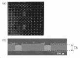
도 2는 본 발명의 실시예에서 제조한 매립기판을 위에서 관찰한 사진(a)과 단면을 전자현미경으로 관찰한 사진(b).
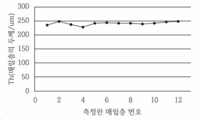
도 3은 본 발명의 실시예에서 제조한 매립기판의 1번 내지 12번 관통공에 매립된 매립층의 두께를 측정한 결과를 보여주는 그래프.

110: 관통공
200: 전극판 210: 전기전도성층
220: 전극기판 290: 적층체
300: 매립기판, 관통공이 매립된 절연성기판
310: 매립층 390: 매립적층체
Th: 매립층의 두께
Claims (9)
- 적어도 1 이상의 관통공이 포함된 패턴을 갖는 절연성기판의 일면을, 전기전도성층을 포함하는 전극판의 전기전도성층 상에 위치시켜 적층체를 형성하는 적층단계; 전기전도성인 금속이온 또는 금속을 포함하는 도금조에 상기 적층체를 위치시키는 설정단계; 상기 도금조에 전류를 인가하여, 전기전도성 금속을 포함하는 매립층이 미리 설정된 두께로 상기 관통공 내에 형성된 것인 매립적층체를 마련하는 도금단계; 그리고 상기 매립적층체에서 상기 절연성 기판과 상기 전극기판을 분리하여 매립된 관통공이 포함된 패턴을 갖는 절연성기판인 매립기판을 제조하는 분리단계;를 포함하여,
12개의 관통공을 기준으로 평가한 상기 매립층 두께의 표준편차가 두께 평균값의 4 % 이하인, 관통공이 매립된 절연성기판의 제조방법. - 제1항에 있어서,
상기 전극판의 전기전도성층이 위치하는 면에서의 제곱평균제곱근조도(Sq) 값은 0.1 내지 300 nm인 것인, 관통공이 매립된 절연성기판의 제조방법. - 제1항에 있어서,
상기 전기전도성층은 상기 매립층 형성의 시드를 포함하는, 관통공이 매립된 절연성기판의 제조방법. - 제3항에 있어서,
상기 전기전도성층은 크롬산화물층, 티타늄산화물층, 이리듐산화물층 및 이들의 조합으로 이루어진 군에서 선택된 어느 하나인, 관통공이 매립된 절연성기판의 제조방법. - 제1항에 있어서,
상기 매립층에 포함되는 전기전도성 금속은 구리, 금, 은, 니켈, 아연, 납, 주석, 코발트 및 이들의 조합으로 이루어진 군에서 선택된 어느 하나를 포함하는, 관통공이 매립된 절연성기판의 제조방법. - 제1항에 있어서,
상기 도금조에 포함되는 금속이온 또는 금속은 도금액에 함유된 형태로 포함되며, 상기 도금액에는 도금억제제를 1,000 ppm 이하로 더 포함하는, 관통공이 매립된 절연성기판의 제조방법. - 제6항에 있어서,
상기 도금억제제는 폴리옥시에틸렌-폴리옥시프로필렌 글리콜, 폴리프로필렌 글리콜, 벤조트리아졸 및 이들의 조합으로 이루어진 군에서 선택된 어느 하나를 포함하고, 상기 도금액은 결정립 크기를 제어하는 미세화 첨가제로 비스-(3-술포프로필)디설파이드, 또는 3-머캅토-1-프로판 술포닉산을 포함하는, 관통공이 매립된 절연성기판의 제조방법. - 제1항에 있어서,
상기 매립층은 전기전도성 금속으로 구리를 포함하고,
상기 도금조에 포함되는 도금액은, 황산구리 0.1 내지 1 mol/L, 전도보조제로 황산 0.5 내지 3 mol/L, 염소이온으로 1 내지 130 ppm, 그리고 도금억제제 10 내지 700 ppm을 포함하는, 관통공이 매립된 절연성기판의 제조방법. - 제1항에 있어서,
상기 도금단계는 20 내지 60 ℃의 상기 도금조 내의 온도 조건 하에 10 내지 100 ㎃/㎠의 전류밀도로 전류를 인가하며 진행되는, 관통공이 매립된 절연성기판의 제조방법.
Applications Claiming Priority (2)
| Application Number | Priority Date | Filing Date | Title |
|---|---|---|---|
| KR1020180147642 | 2018-11-26 | ||
| KR20180147642 | 2018-11-26 |
Publications (2)
| Publication Number | Publication Date |
|---|---|
| KR20200062001A true KR20200062001A (ko) | 2020-06-03 |
| KR102178158B1 KR102178158B1 (ko) | 2020-11-12 |
Family
ID=71087705
Family Applications (1)
| Application Number | Title | Priority Date | Filing Date |
|---|---|---|---|
| KR1020190002370A Active KR102178158B1 (ko) | 2018-11-26 | 2019-01-08 | 관통공이 매립된 Si 기판의 제조방법 |
Country Status (1)
| Country | Link |
|---|---|
| KR (1) | KR102178158B1 (ko) |
Cited By (1)
| Publication number | Priority date | Publication date | Assignee | Title |
|---|---|---|---|---|
| KR20240099519A (ko) * | 2022-12-21 | 2024-07-01 | (재)한국나노기술원 | 3차원 소자 제작을 위한 미세 관통 전극이 형성된 투명 기판 및 그 제조 방법 |
Citations (7)
| Publication number | Priority date | Publication date | Assignee | Title |
|---|---|---|---|---|
| JPH0547701A (ja) * | 1991-08-13 | 1993-02-26 | Dainippon Printing Co Ltd | 微細パターンの形成方法 |
| JP2002198390A (ja) * | 2000-10-20 | 2002-07-12 | Sumitomo Special Metals Co Ltd | 転写用はんだバンプシートおよびその製造方法、ならびに半導体装置およびプリント基板の製造方法 |
| JP2008021739A (ja) * | 2006-07-11 | 2008-01-31 | Shinko Electric Ind Co Ltd | 基板の製造方法 |
| KR20090110712A (ko) * | 2008-04-18 | 2009-10-22 | 성균관대학교산학협력단 | 알루미늄 호일을 이용한 관통형 전극 형성방법 |
| JP2012124253A (ja) * | 2010-12-07 | 2012-06-28 | Canon Inc | 貫通電極基板及びその製造方法 |
| JP2012195465A (ja) | 2011-03-17 | 2012-10-11 | Canon Inc | 貫通電極基板及びその製造方法 |
| JP2014095104A (ja) * | 2012-11-07 | 2014-05-22 | Toppan Printing Co Ltd | めっきによる貫通孔の銅充填方法 |
-
2019
- 2019-01-08 KR KR1020190002370A patent/KR102178158B1/ko active Active
Patent Citations (7)
| Publication number | Priority date | Publication date | Assignee | Title |
|---|---|---|---|---|
| JPH0547701A (ja) * | 1991-08-13 | 1993-02-26 | Dainippon Printing Co Ltd | 微細パターンの形成方法 |
| JP2002198390A (ja) * | 2000-10-20 | 2002-07-12 | Sumitomo Special Metals Co Ltd | 転写用はんだバンプシートおよびその製造方法、ならびに半導体装置およびプリント基板の製造方法 |
| JP2008021739A (ja) * | 2006-07-11 | 2008-01-31 | Shinko Electric Ind Co Ltd | 基板の製造方法 |
| KR20090110712A (ko) * | 2008-04-18 | 2009-10-22 | 성균관대학교산학협력단 | 알루미늄 호일을 이용한 관통형 전극 형성방법 |
| JP2012124253A (ja) * | 2010-12-07 | 2012-06-28 | Canon Inc | 貫通電極基板及びその製造方法 |
| JP2012195465A (ja) | 2011-03-17 | 2012-10-11 | Canon Inc | 貫通電極基板及びその製造方法 |
| JP2014095104A (ja) * | 2012-11-07 | 2014-05-22 | Toppan Printing Co Ltd | めっきによる貫通孔の銅充填方法 |
Cited By (1)
| Publication number | Priority date | Publication date | Assignee | Title |
|---|---|---|---|---|
| KR20240099519A (ko) * | 2022-12-21 | 2024-07-01 | (재)한국나노기술원 | 3차원 소자 제작을 위한 미세 관통 전극이 형성된 투명 기판 및 그 제조 방법 |
Also Published As
| Publication number | Publication date |
|---|---|
| KR102178158B1 (ko) | 2020-11-12 |
Similar Documents
| Publication | Publication Date | Title |
|---|---|---|
| CN102318041B (zh) | 用于电沉积铜的工艺,在穿硅通孔(tsv)中的芯片间、芯片到晶片间和晶片间的互连 | |
| CN103730445A (zh) | 具有双晶铜线路层的电路板及其制作方法 | |
| CN106298634A (zh) | 一种定向生长纳米孪晶铜的通孔填充方法及其应用 | |
| TW201127231A (en) | Metal deposition | |
| MXPA00005871A (es) | ELECTRODEPOSICION DE METALES EN RECESOS PEQUEnOS USANDO CAMPOS ELECTRICOS MODULADOS. | |
| TW201220968A (en) | Multilayer wiring board | |
| CN101263247A (zh) | 用于使用金属涂布基底表面的电镀组合物 | |
| JP2010171170A (ja) | 銅回路配線基板およびその製造方法 | |
| TW201125038A (en) | Metal deposition | |
| JP2011520039A (ja) | 電着組成物、及び、該組成物を用いた半導体基板のコーティング方法 | |
| KR20220047373A (ko) | 고밀도 인터커넥트 인쇄 회로 기판의 제조 시퀀스 및 고밀도 인터커넥트 인쇄 회로 기판 | |
| TW200529328A (en) | Electroplating apparatus | |
| TW201201322A (en) | Seed layer deposition in microscale features | |
| KR102178158B1 (ko) | 관통공이 매립된 Si 기판의 제조방법 | |
| US6841458B2 (en) | Dopant interface formation | |
| JPH11298141A (ja) | 電子装置の製造方法 | |
| KR101239430B1 (ko) | 전해 연마를 이용한 기판의 평탄화 방법 및 이를 포함하는 반도체 소자의 제조 방법 | |
| JP4472673B2 (ja) | 銅配線の製造方法及び銅めっき用電解液 | |
| JP5671317B2 (ja) | 貫通電極基板及びその製造方法 | |
| JP4429585B2 (ja) | 選択的絶縁方法及び貫通ビアを備えた実装基板 | |
| US12293966B2 (en) | Conductive structure including copper-phosphorous alloy and a method of manufacturing conductive structure | |
| JP2002368384A (ja) | 配線基板または半導体回路の製造方法 | |
| KR100472856B1 (ko) | 반도체 소자의 금속 배선 형성 방법 | |
| TWI653364B (zh) | 免熱處理製備超大晶粒銅之方法、電解液、包含超大晶粒銅之銅箔及電子元件連接結構 | |
| KR20240176568A (ko) | 유리 관통 비아형 금속배선 형성방법 및 이를 이용한 인터포저의 제조방법 |
Legal Events
| Date | Code | Title | Description |
|---|---|---|---|
| A201 | Request for examination | ||
| PA0109 | Patent application |
St.27 status event code: A-0-1-A10-A12-nap-PA0109 |
|
| PA0201 | Request for examination |
St.27 status event code: A-1-2-D10-D11-exm-PA0201 |
|
| D13-X000 | Search requested |
St.27 status event code: A-1-2-D10-D13-srh-X000 |
|
| D14-X000 | Search report completed |
St.27 status event code: A-1-2-D10-D14-srh-X000 |
|
| E902 | Notification of reason for refusal | ||
| PE0902 | Notice of grounds for rejection |
St.27 status event code: A-1-2-D10-D21-exm-PE0902 |
|
| E13-X000 | Pre-grant limitation requested |
St.27 status event code: A-2-3-E10-E13-lim-X000 |
|
| P11-X000 | Amendment of application requested |
St.27 status event code: A-2-2-P10-P11-nap-X000 |
|
| P13-X000 | Application amended |
St.27 status event code: A-2-2-P10-P13-nap-X000 |
|
| PG1501 | Laying open of application |
St.27 status event code: A-1-1-Q10-Q12-nap-PG1501 |
|
| E90F | Notification of reason for final refusal | ||
| PE0902 | Notice of grounds for rejection |
St.27 status event code: A-1-2-D10-D21-exm-PE0902 |
|
| P11-X000 | Amendment of application requested |
St.27 status event code: A-2-2-P10-P11-nap-X000 |
|
| P13-X000 | Application amended |
St.27 status event code: A-2-2-P10-P13-nap-X000 |
|
| E701 | Decision to grant or registration of patent right | ||
| PE0701 | Decision of registration |
St.27 status event code: A-1-2-D10-D22-exm-PE0701 |
|
| GRNT | Written decision to grant | ||
| PR0701 | Registration of establishment |
St.27 status event code: A-2-4-F10-F11-exm-PR0701 |
|
| PR1002 | Payment of registration fee |
St.27 status event code: A-2-2-U10-U11-oth-PR1002 Fee payment year number: 1 |
|
| PG1601 | Publication of registration |
St.27 status event code: A-4-4-Q10-Q13-nap-PG1601 |
|
| R18-X000 | Changes to party contact information recorded |
St.27 status event code: A-5-5-R10-R18-oth-X000 |
|
| PR1001 | Payment of annual fee |
St.27 status event code: A-4-4-U10-U11-oth-PR1001 Fee payment year number: 4 |
|
| PR1001 | Payment of annual fee |
St.27 status event code: A-4-4-U10-U11-oth-PR1001 Fee payment year number: 5 |
|
| P22-X000 | Classification modified |
St.27 status event code: A-4-4-P10-P22-nap-X000 |
|
| PN2301 | Change of applicant |
St.27 status event code: A-5-5-R10-R11-asn-PN2301 |
|
| R11 | Change to the name of applicant or owner or transfer of ownership requested |
Free format text: ST27 STATUS EVENT CODE: A-5-5-R10-R11-ASN-PN2301 (AS PROVIDED BY THE NATIONAL OFFICE) |
|
| PN2301 | Change of applicant |
St.27 status event code: A-5-5-R10-R14-asn-PN2301 |
|
| R14 | Transfer of ownership recorded |
Free format text: ST27 STATUS EVENT CODE: A-5-5-R10-R14-ASN-PN2301 (AS PROVIDED BY THE NATIONAL OFFICE) |
|
| R18 | Changes to party contact information recorded |
Free format text: ST27 STATUS EVENT CODE: A-5-5-R10-R18-OTH-X000 (AS PROVIDED BY THE NATIONAL OFFICE) |
|
| R18-X000 | Changes to party contact information recorded |
St.27 status event code: A-5-5-R10-R18-oth-X000 |
|
| P14 | Amendment of ip right document requested |
Free format text: ST27 STATUS EVENT CODE: A-5-5-P10-P14-NAP-X000 (AS PROVIDED BY THE NATIONAL OFFICE) |
|
| P14-X000 | Amendment of ip right document requested |
St.27 status event code: A-5-5-P10-P14-nap-X000 |
|
| PN2301 | Change of applicant |
St.27 status event code: A-5-5-R10-R11-asn-PN2301 |
|
| R11 | Change to the name of applicant or owner or transfer of ownership requested |
Free format text: ST27 STATUS EVENT CODE: A-5-5-R10-R11-ASN-PN2301 (AS PROVIDED BY THE NATIONAL OFFICE) |
|
| P16 | Ip right document amended |
Free format text: ST27 STATUS EVENT CODE: A-5-5-P10-P16-NAP-X000 (AS PROVIDED BY THE NATIONAL OFFICE) |
|
| P16-X000 | Ip right document amended |
St.27 status event code: A-5-5-P10-P16-nap-X000 |
|
| PN2301 | Change of applicant |
St.27 status event code: A-5-5-R10-R14-asn-PN2301 |
|
| R14 | Transfer of ownership recorded |
Free format text: ST27 STATUS EVENT CODE: A-5-5-R10-R14-ASN-PN2301 (AS PROVIDED BY THE NATIONAL OFFICE) |