KR20200069231A - 플라스마 처리 장치 및 플라스마 처리 방법 - Google Patents
플라스마 처리 장치 및 플라스마 처리 방법 Download PDFInfo
- Publication number
- KR20200069231A KR20200069231A KR1020190156374A KR20190156374A KR20200069231A KR 20200069231 A KR20200069231 A KR 20200069231A KR 1020190156374 A KR1020190156374 A KR 1020190156374A KR 20190156374 A KR20190156374 A KR 20190156374A KR 20200069231 A KR20200069231 A KR 20200069231A
- Authority
- KR
- South Korea
- Prior art keywords
- gas
- upper electrode
- plasma processing
- processing
- processing apparatus
- Prior art date
- Legal status (The legal status is an assumption and is not a legal conclusion. Google has not performed a legal analysis and makes no representation as to the accuracy of the status listed.)
- Granted
Links
Images


Classifications
-
- H—ELECTRICITY
- H01—ELECTRIC ELEMENTS
- H01J—ELECTRIC DISCHARGE TUBES OR DISCHARGE LAMPS
- H01J37/00—Discharge tubes with provision for introducing objects or material to be exposed to the discharge, e.g. for the purpose of examination or processing thereof
- H01J37/32—Gas-filled discharge tubes
- H01J37/32431—Constructional details of the reactor
- H01J37/3244—Gas supply means
- H01J37/32449—Gas control, e.g. control of the gas flow
-
- H—ELECTRICITY
- H01—ELECTRIC ELEMENTS
- H01J—ELECTRIC DISCHARGE TUBES OR DISCHARGE LAMPS
- H01J37/00—Discharge tubes with provision for introducing objects or material to be exposed to the discharge, e.g. for the purpose of examination or processing thereof
- H01J37/32—Gas-filled discharge tubes
- H01J37/32431—Constructional details of the reactor
- H01J37/3244—Gas supply means
-
- H—ELECTRICITY
- H01—ELECTRIC ELEMENTS
- H01J—ELECTRIC DISCHARGE TUBES OR DISCHARGE LAMPS
- H01J37/00—Discharge tubes with provision for introducing objects or material to be exposed to the discharge, e.g. for the purpose of examination or processing thereof
- H01J37/32—Gas-filled discharge tubes
- H01J37/32431—Constructional details of the reactor
- H01J37/32532—Electrodes
- H01J37/32568—Relative arrangement or disposition of electrodes; moving means
-
- H—ELECTRICITY
- H10—SEMICONDUCTOR DEVICES; ELECTRIC SOLID-STATE DEVICES NOT OTHERWISE PROVIDED FOR
- H10P—GENERIC PROCESSES OR APPARATUS FOR THE MANUFACTURE OR TREATMENT OF DEVICES COVERED BY CLASS H10
- H10P72/00—Handling or holding of wafers, substrates or devices during manufacture or treatment thereof
- H10P72/04—Apparatus for manufacture or treatment
- H10P72/0402—Apparatus for fluid treatment
- H10P72/0418—Apparatus for fluid treatment for etching
- H10P72/0421—Apparatus for fluid treatment for etching for drying etching
-
- H—ELECTRICITY
- H10—SEMICONDUCTOR DEVICES; ELECTRIC SOLID-STATE DEVICES NOT OTHERWISE PROVIDED FOR
- H10P—GENERIC PROCESSES OR APPARATUS FOR THE MANUFACTURE OR TREATMENT OF DEVICES COVERED BY CLASS H10
- H10P72/00—Handling or holding of wafers, substrates or devices during manufacture or treatment thereof
- H10P72/70—Handling or holding of wafers, substrates or devices during manufacture or treatment thereof for supporting or gripping
- H10P72/76—Handling or holding of wafers, substrates or devices during manufacture or treatment thereof for supporting or gripping using mechanical means, e.g. clamps or pinches
- H10P72/7604—Handling or holding of wafers, substrates or devices during manufacture or treatment thereof for supporting or gripping using mechanical means, e.g. clamps or pinches the wafers being placed on a susceptor, stage or support
- H10P72/7612—Handling or holding of wafers, substrates or devices during manufacture or treatment thereof for supporting or gripping using mechanical means, e.g. clamps or pinches the wafers being placed on a susceptor, stage or support characterised by lifting arrangements, e.g. lift pins
-
- H—ELECTRICITY
- H01—ELECTRIC ELEMENTS
- H01J—ELECTRIC DISCHARGE TUBES OR DISCHARGE LAMPS
- H01J2237/00—Discharge tubes exposing object to beam, e.g. for analysis treatment, etching, imaging
- H01J2237/006—Details of gas supplies, e.g. in an ion source, to a beam line, to a specimen or to a workpiece
-
- H—ELECTRICITY
- H01—ELECTRIC ELEMENTS
- H01J—ELECTRIC DISCHARGE TUBES OR DISCHARGE LAMPS
- H01J2237/00—Discharge tubes exposing object to beam, e.g. for analysis treatment, etching, imaging
- H01J2237/32—Processing objects by plasma generation
- H01J2237/33—Processing objects by plasma generation characterised by the type of processing
- H01J2237/334—Etching
-
- H—ELECTRICITY
- H01—ELECTRIC ELEMENTS
- H01J—ELECTRIC DISCHARGE TUBES OR DISCHARGE LAMPS
- H01J37/00—Discharge tubes with provision for introducing objects or material to be exposed to the discharge, e.g. for the purpose of examination or processing thereof
- H01J37/32—Gas-filled discharge tubes
- H01J37/32009—Arrangements for generation of plasma specially adapted for examination or treatment of objects, e.g. plasma sources
- H01J37/32082—Radio frequency generated discharge
Landscapes
- Physics & Mathematics (AREA)
- Engineering & Computer Science (AREA)
- Plasma & Fusion (AREA)
- Chemical & Material Sciences (AREA)
- Analytical Chemistry (AREA)
- Plasma Technology (AREA)
- Drying Of Semiconductors (AREA)
- Chemical Vapour Deposition (AREA)
Abstract
처리 용기 내의 기판에 대하여 플라스마 처리를 행하는 플라스마 처리 장치이며, 상기 처리 용기 내의 상방에 배치된 상부 전극과, 정합기를 통하여 플라스마원으로부터의 고주파 전력을, 상기 상부 전극의 중심에 공급하기 위한 급전봉과, 복수의 토출 구멍을 갖고, 상기 상부 전극의 하방에 배치된 가스 확산판과, 상기 처리 용기 내에 처리 가스를 도입하는 가스 도입 부재를 갖고, 상기 가스 도입 부재는, 상기 상부 전극의 상방에 배치되며, 또한 가스 유로가 내부에 형성된 상기 급전봉을 둘러싸는 형상의 원환부를 갖고, 상기 원환부의 하측에는, 통형의 절연 도입 부재가 마련되고, 상기 절연 도입 부재의 내부에는, 상기 가스 유로와 연통되며 상하 방향으로 형성된 2 이상의 가스 공급로가 형성되고, 상기 상부 전극과 급전봉의 접속부의 바로 밑에는, 상기 가스 공급로로부터의 처리 가스를 합류시키는 합류부가 마련되고, 당해 합류부에서 합류된 후의 처리 가스가, 상기 가스 확산판의 상측에 형성되며 상기 토출 구멍에 연통되는 공간으로 흐르도록 구성되어 있다.
Description
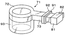
도 2는, 도 1의 플라스마 처리 장치에 있어서의 가스 도입 부재의 사시도이다.
도 3은, 도 1의 플라스마 처리 장치에 있어서의 가스 도입 부재의 평면의 설명도이다.
도 4는, 도 1의 플라스마 처리 장치에 있어서의 절연 도입 부재의 종단면도이다.
도 5는, 도 1의 플라스마 처리 장치에 사용 가능한 다른 절연 도입 부재의 종단면도이다.
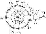
도 6은, 다른 실시 형태에 관한 플라스마 처리 장치에 있어서의 상부 전극의 측면 단면의 설명도이다.
도 7은, 도 1의 플라스마 처리 장치에 사용 가능한 다른 가스 도입 부재의 평면의 설명도이다.
Claims (6)
- 처리 용기 내의 기판에 대하여 플라스마 처리를 행하는 플라스마 처리 장치이며,
상기 처리 용기 내의 상방에 배치된 상부 전극과,
정합기를 통하여 플라스마원으로부터의 고주파 전력을, 상기 상부 전극의 중심에 공급하기 위한 급전봉과,
복수의 토출 구멍을 갖고, 상기 상부 전극의 하방에 배치된 가스 확산판과,
상기 처리 용기 내에 처리 가스를 도입하는 가스 도입 부재를 포함하고,
상기 가스 도입 부재는, 상기 상부 전극의 상방에 배치되며, 가스 유로가 내부에 형성되고 상기 급전봉을 둘러싸는 형상의 원환부를 포함하고,
상기 플라스마 처리 장치는, 상기 원환부의 하측에 마련된 통형의 절연 도입 부재를 더 포함하고,
상기 절연 도입 부재의 내부에는, 상기 가스 유로와 연통되며 상하 방향으로 형성된 2 이상의 가스 공급로가 형성되고,
상기 상부 전극과 급전봉의 접속부의 바로 밑에는, 상기 가스 공급로로부터의 처리 가스를 합류시키는 합류부가 마련되고,
당해 합류부에서 합류된 후의 처리 가스가, 상기 가스 확산판의 상측에 형성되며 상기 토출 구멍에 연통되는 공간으로 흐르도록 구성된, 플라스마 처리 장치. - 제1항에 있어서,
상기 가스 유로로부터 상기 원환부를 따라 원호형으로 분기된 가스 유로는, 상기 절연 도입 부재의 상기 가스 공급로와 각각 접속되어 있는, 플라스마 처리 장치. - 제1항 또는 제2항에 있어서,
상기 가스 공급로의 상하 단부 상호간은 직선형으로 꿰뚫어 볼 수 없도록, 상기 가스 공급로가 상기 절연 도입 부재의 내부에 형성되어 있는, 플라스마 처리 장치. - 제3항에 있어서,
상기 가스 공급로는, 상기 절연 도입 부재에서 도중에 외측으로 절곡되는 절곡부를 포함하는, 플라스마 처리 장치. - 제1항 내지 제4항 중 어느 한 항에 있어서,
상기 합류부와 상기 공간의 사이에 마련되어 있고, 상기 합류부로부터의 처리 가스를 분산시켜 상기 공간으로 흘리는 분산 유로를 더 포함하는, 플라스마 처리 장치. - 제1항 내지 제5항 중 어느 한 항에 기재된 플라스마 처리 장치를 사용하여, 상기 처리 용기 내의 기판에 대하여 플라스마 처리를 행하는, 플라스마 처리 방법.
Applications Claiming Priority (2)
| Application Number | Priority Date | Filing Date | Title |
|---|---|---|---|
| JPJP-P-2018-228867 | 2018-12-06 | ||
| JP2018228867A JP7105180B2 (ja) | 2018-12-06 | 2018-12-06 | プラズマ処理装置及びプラズマ処理方法 |
Publications (2)
| Publication Number | Publication Date |
|---|---|
| KR20200069231A true KR20200069231A (ko) | 2020-06-16 |
| KR102224427B1 KR102224427B1 (ko) | 2021-03-05 |
Family
ID=70972108
Family Applications (1)
| Application Number | Title | Priority Date | Filing Date |
|---|---|---|---|
| KR1020190156374A Active KR102224427B1 (ko) | 2018-12-06 | 2019-11-29 | 플라스마 처리 장치 및 플라스마 처리 방법 |
Country Status (5)
| Country | Link |
|---|---|
| US (1) | US10950415B2 (ko) |
| JP (1) | JP7105180B2 (ko) |
| KR (1) | KR102224427B1 (ko) |
| CN (1) | CN111293027B (ko) |
| TW (1) | TW202101540A (ko) |
Families Citing this family (3)
| Publication number | Priority date | Publication date | Assignee | Title |
|---|---|---|---|---|
| JP7450475B2 (ja) * | 2020-06-30 | 2024-03-15 | 東京エレクトロン株式会社 | プラズマ処理装置 |
| JP2022048825A (ja) | 2020-09-15 | 2022-03-28 | 東京エレクトロン株式会社 | プラズマ処理装置及び半導体デバイスの製造方法 |
| JP2022119578A (ja) * | 2021-02-04 | 2022-08-17 | 東京エレクトロン株式会社 | プラズマ処理装置 |
Citations (5)
| Publication number | Priority date | Publication date | Assignee | Title |
|---|---|---|---|---|
| JPH0595037U (ja) * | 1992-05-27 | 1993-12-24 | 株式会社島津製作所 | プラズマcvd装置 |
| JP2000331996A (ja) * | 1999-05-21 | 2000-11-30 | Tokyo Electron Ltd | プラズマ処理装置 |
| JP2003257937A (ja) | 2002-02-27 | 2003-09-12 | Tokyo Electron Ltd | プラズマ処理装置 |
| KR20180072551A (ko) * | 2016-12-21 | 2018-06-29 | 도쿄엘렉트론가부시키가이샤 | 가스 처리 장치 및 가스 처리 방법 |
| KR20180088496A (ko) * | 2013-11-06 | 2018-08-03 | 어플라이드 머티어리얼스, 인코포레이티드 | Dc 바이어스 변조에 의한 입자 발생 억제기 |
Family Cites Families (6)
| Publication number | Priority date | Publication date | Assignee | Title |
|---|---|---|---|---|
| JPH10172792A (ja) * | 1996-12-05 | 1998-06-26 | Tokyo Electron Ltd | プラズマ処理装置 |
| JP3438696B2 (ja) | 2000-03-13 | 2003-08-18 | 松下電器産業株式会社 | プラズマ処理方法及び装置 |
| JP2005116901A (ja) | 2003-10-09 | 2005-04-28 | Sekisui Chem Co Ltd | プラズマ成膜装置 |
| JP5614180B2 (ja) * | 2010-09-01 | 2014-10-29 | 東レ株式会社 | プラズマcvd装置 |
| JP6078354B2 (ja) * | 2013-01-24 | 2017-02-08 | 東京エレクトロン株式会社 | プラズマ処理装置 |
| JP6696322B2 (ja) * | 2016-06-24 | 2020-05-20 | 東京エレクトロン株式会社 | ガス処理装置、ガス処理方法及び記憶媒体 |
-
2018
- 2018-12-06 JP JP2018228867A patent/JP7105180B2/ja active Active
-
2019
- 2019-11-27 TW TW108143082A patent/TW202101540A/zh unknown
- 2019-11-29 KR KR1020190156374A patent/KR102224427B1/ko active Active
- 2019-12-04 US US16/703,393 patent/US10950415B2/en active Active
- 2019-12-05 CN CN201911233093.1A patent/CN111293027B/zh active Active
Patent Citations (5)
| Publication number | Priority date | Publication date | Assignee | Title |
|---|---|---|---|---|
| JPH0595037U (ja) * | 1992-05-27 | 1993-12-24 | 株式会社島津製作所 | プラズマcvd装置 |
| JP2000331996A (ja) * | 1999-05-21 | 2000-11-30 | Tokyo Electron Ltd | プラズマ処理装置 |
| JP2003257937A (ja) | 2002-02-27 | 2003-09-12 | Tokyo Electron Ltd | プラズマ処理装置 |
| KR20180088496A (ko) * | 2013-11-06 | 2018-08-03 | 어플라이드 머티어리얼스, 인코포레이티드 | Dc 바이어스 변조에 의한 입자 발생 억제기 |
| KR20180072551A (ko) * | 2016-12-21 | 2018-06-29 | 도쿄엘렉트론가부시키가이샤 | 가스 처리 장치 및 가스 처리 방법 |
Also Published As
| Publication number | Publication date |
|---|---|
| CN111293027A (zh) | 2020-06-16 |
| US10950415B2 (en) | 2021-03-16 |
| TW202101540A (zh) | 2021-01-01 |
| US20200185199A1 (en) | 2020-06-11 |
| KR102224427B1 (ko) | 2021-03-05 |
| JP2020092177A (ja) | 2020-06-11 |
| CN111293027B (zh) | 2023-03-10 |
| JP7105180B2 (ja) | 2022-07-22 |
Similar Documents
| Publication | Publication Date | Title |
|---|---|---|
| JP6936884B2 (ja) | 改良されたフロー均一性/ガスコンダクタンスを備えた可変処理容積に対処するための対称チャンバ本体設計アーキテクチャ | |
| KR102121655B1 (ko) | 플라즈마 처리 장치 | |
| KR101361757B1 (ko) | 대칭적인 플라즈마 프로세스 챔버 | |
| KR102220276B1 (ko) | 플라스마 처리 장치 및 플라스마 처리 방법 | |
| US20090159002A1 (en) | Gas distribution plate with annular plenum having a sloped ceiling for uniform distribution | |
| KR101672856B1 (ko) | 플라즈마 처리 장치 | |
| US20140083615A1 (en) | Antenna assembly and a plasma processing chamber having the same | |
| US20100230052A1 (en) | Shower head and plasma processing apparatus having same | |
| US20180144945A1 (en) | Placing unit and plasma processing apparatus | |
| KR102585041B1 (ko) | 플라스마 처리 장치 | |
| KR20200069231A (ko) | 플라스마 처리 장치 및 플라스마 처리 방법 | |
| TW202518520A (zh) | 電漿處理裝置 | |
| KR20200051505A (ko) | 배치대 및 기판 처리 장치 | |
| KR20240104212A (ko) | 플라스마 처리 장치 및 플라스마 처리 방법 | |
| CN113013012B (zh) | 隔挡部件及基板处理装置 | |
| US20150176125A1 (en) | Substrate processing apparatus | |
| KR102775903B1 (ko) | 다수의 공정 챔버를 구비한 기판 처리 장치 | |
| CN112563110A (zh) | 等离子体处理装置 | |
| KR102500590B1 (ko) | 플라즈마 처리 장치 | |
| KR20240134852A (ko) | 플라스마 처리 장치 및 플라스마 처리 장치의 시료대의 제조 방법 |
Legal Events
| Date | Code | Title | Description |
|---|---|---|---|
| PA0109 | Patent application |
Patent event code: PA01091R01D Comment text: Patent Application Patent event date: 20191129 |
|
| PA0201 | Request for examination | ||
| PG1501 | Laying open of application | ||
| E902 | Notification of reason for refusal | ||
| PE0902 | Notice of grounds for rejection |
Comment text: Notification of reason for refusal Patent event date: 20200915 Patent event code: PE09021S01D |
|
| E701 | Decision to grant or registration of patent right | ||
| PE0701 | Decision of registration |
Patent event code: PE07011S01D Comment text: Decision to Grant Registration Patent event date: 20201208 |
|
| GRNT | Written decision to grant | ||
| PR0701 | Registration of establishment |
Comment text: Registration of Establishment Patent event date: 20210302 Patent event code: PR07011E01D |
|
| PR1002 | Payment of registration fee |
Payment date: 20210302 End annual number: 3 Start annual number: 1 |
|
| PG1601 | Publication of registration | ||
| PR1001 | Payment of annual fee |
Payment date: 20240219 Start annual number: 4 End annual number: 4 |