KR20200074647A - 메모리 시스템 및 그것의 동작방법 - Google Patents
메모리 시스템 및 그것의 동작방법 Download PDFInfo
- Publication number
- KR20200074647A KR20200074647A KR1020180163281A KR20180163281A KR20200074647A KR 20200074647 A KR20200074647 A KR 20200074647A KR 1020180163281 A KR1020180163281 A KR 1020180163281A KR 20180163281 A KR20180163281 A KR 20180163281A KR 20200074647 A KR20200074647 A KR 20200074647A
- Authority
- KR
- South Korea
- Prior art keywords
- memory
- mapping information
- unmap
- logical address
- map
- Prior art date
- Legal status (The legal status is an assumption and is not a legal conclusion. Google has not performed a legal analysis and makes no representation as to the accuracy of the status listed.)
- Granted
Links
Images









Classifications
-
- G—PHYSICS
- G06—COMPUTING OR CALCULATING; COUNTING
- G06F—ELECTRIC DIGITAL DATA PROCESSING
- G06F12/00—Accessing, addressing or allocating within memory systems or architectures
- G06F12/02—Addressing or allocation; Relocation
- G06F12/0223—User address space allocation, e.g. contiguous or non contiguous base addressing
- G06F12/023—Free address space management
- G06F12/0238—Memory management in non-volatile memory, e.g. resistive RAM or ferroelectric memory
- G06F12/0246—Memory management in non-volatile memory, e.g. resistive RAM or ferroelectric memory in block erasable memory, e.g. flash memory
-
- G—PHYSICS
- G06—COMPUTING OR CALCULATING; COUNTING
- G06F—ELECTRIC DIGITAL DATA PROCESSING
- G06F12/00—Accessing, addressing or allocating within memory systems or architectures
- G06F12/02—Addressing or allocation; Relocation
- G06F12/0223—User address space allocation, e.g. contiguous or non contiguous base addressing
- G06F12/023—Free address space management
-
- G—PHYSICS
- G06—COMPUTING OR CALCULATING; COUNTING
- G06F—ELECTRIC DIGITAL DATA PROCESSING
- G06F12/00—Accessing, addressing or allocating within memory systems or architectures
- G06F12/02—Addressing or allocation; Relocation
- G06F12/06—Addressing a physical block of locations, e.g. base addressing, module addressing, memory dedication
- G06F12/0646—Configuration or reconfiguration
-
- G—PHYSICS
- G06—COMPUTING OR CALCULATING; COUNTING
- G06F—ELECTRIC DIGITAL DATA PROCESSING
- G06F12/00—Accessing, addressing or allocating within memory systems or architectures
- G06F12/02—Addressing or allocation; Relocation
- G06F12/08—Addressing or allocation; Relocation in hierarchically structured memory systems, e.g. virtual memory systems
- G06F12/0802—Addressing of a memory level in which the access to the desired data or data block requires associative addressing means, e.g. caches
- G06F12/0866—Addressing of a memory level in which the access to the desired data or data block requires associative addressing means, e.g. caches for peripheral storage systems, e.g. disk cache
- G06F12/0873—Mapping of cache memory to specific storage devices or parts thereof
-
- G—PHYSICS
- G06—COMPUTING OR CALCULATING; COUNTING
- G06F—ELECTRIC DIGITAL DATA PROCESSING
- G06F12/00—Accessing, addressing or allocating within memory systems or architectures
- G06F12/02—Addressing or allocation; Relocation
- G06F12/08—Addressing or allocation; Relocation in hierarchically structured memory systems, e.g. virtual memory systems
- G06F12/10—Address translation
-
- G—PHYSICS
- G06—COMPUTING OR CALCULATING; COUNTING
- G06F—ELECTRIC DIGITAL DATA PROCESSING
- G06F3/00—Input arrangements for transferring data to be processed into a form capable of being handled by the computer; Output arrangements for transferring data from processing unit to output unit, e.g. interface arrangements
- G06F3/06—Digital input from, or digital output to, record carriers, e.g. RAID, emulated record carriers or networked record carriers
- G06F3/0601—Interfaces specially adapted for storage systems
- G06F3/0628—Interfaces specially adapted for storage systems making use of a particular technique
- G06F3/0638—Organizing or formatting or addressing of data
- G06F3/064—Management of blocks
-
- G—PHYSICS
- G06—COMPUTING OR CALCULATING; COUNTING
- G06F—ELECTRIC DIGITAL DATA PROCESSING
- G06F3/00—Input arrangements for transferring data to be processed into a form capable of being handled by the computer; Output arrangements for transferring data from processing unit to output unit, e.g. interface arrangements
- G06F3/06—Digital input from, or digital output to, record carriers, e.g. RAID, emulated record carriers or networked record carriers
- G06F3/0601—Interfaces specially adapted for storage systems
- G06F3/0628—Interfaces specially adapted for storage systems making use of a particular technique
- G06F3/0655—Vertical data movement, i.e. input-output transfer; data movement between one or more hosts and one or more storage devices
- G06F3/0658—Controller construction arrangements
-
- G—PHYSICS
- G06—COMPUTING OR CALCULATING; COUNTING
- G06F—ELECTRIC DIGITAL DATA PROCESSING
- G06F12/00—Accessing, addressing or allocating within memory systems or architectures
- G06F12/02—Addressing or allocation; Relocation
- G06F12/08—Addressing or allocation; Relocation in hierarchically structured memory systems, e.g. virtual memory systems
- G06F12/0802—Addressing of a memory level in which the access to the desired data or data block requires associative addressing means, e.g. caches
- G06F12/0866—Addressing of a memory level in which the access to the desired data or data block requires associative addressing means, e.g. caches for peripheral storage systems, e.g. disk cache
- G06F12/0868—Data transfer between cache memory and other subsystems, e.g. storage devices or host systems
-
- G—PHYSICS
- G06—COMPUTING OR CALCULATING; COUNTING
- G06F—ELECTRIC DIGITAL DATA PROCESSING
- G06F12/00—Accessing, addressing or allocating within memory systems or architectures
- G06F12/02—Addressing or allocation; Relocation
- G06F12/08—Addressing or allocation; Relocation in hierarchically structured memory systems, e.g. virtual memory systems
- G06F12/0802—Addressing of a memory level in which the access to the desired data or data block requires associative addressing means, e.g. caches
- G06F12/0866—Addressing of a memory level in which the access to the desired data or data block requires associative addressing means, e.g. caches for peripheral storage systems, e.g. disk cache
- G06F12/0871—Allocation or management of cache space
-
- G—PHYSICS
- G06—COMPUTING OR CALCULATING; COUNTING
- G06F—ELECTRIC DIGITAL DATA PROCESSING
- G06F2212/00—Indexing scheme relating to accessing, addressing or allocation within memory systems or architectures
- G06F2212/10—Providing a specific technical effect
- G06F2212/1016—Performance improvement
-
- G—PHYSICS
- G06—COMPUTING OR CALCULATING; COUNTING
- G06F—ELECTRIC DIGITAL DATA PROCESSING
- G06F2212/00—Indexing scheme relating to accessing, addressing or allocation within memory systems or architectures
- G06F2212/31—Providing disk cache in a specific location of a storage system
- G06F2212/312—In storage controller
-
- G—PHYSICS
- G06—COMPUTING OR CALCULATING; COUNTING
- G06F—ELECTRIC DIGITAL DATA PROCESSING
- G06F2212/00—Indexing scheme relating to accessing, addressing or allocation within memory systems or architectures
- G06F2212/46—Caching storage objects of specific type in disk cache
- G06F2212/466—Metadata, control data
-
- G—PHYSICS
- G06—COMPUTING OR CALCULATING; COUNTING
- G06F—ELECTRIC DIGITAL DATA PROCESSING
- G06F2212/00—Indexing scheme relating to accessing, addressing or allocation within memory systems or architectures
- G06F2212/65—Details of virtual memory and virtual address translation
-
- G—PHYSICS
- G06—COMPUTING OR CALCULATING; COUNTING
- G06F—ELECTRIC DIGITAL DATA PROCESSING
- G06F2212/00—Indexing scheme relating to accessing, addressing or allocation within memory systems or architectures
- G06F2212/65—Details of virtual memory and virtual address translation
- G06F2212/657—Virtual address space management
-
- G—PHYSICS
- G06—COMPUTING OR CALCULATING; COUNTING
- G06F—ELECTRIC DIGITAL DATA PROCESSING
- G06F2212/00—Indexing scheme relating to accessing, addressing or allocation within memory systems or architectures
- G06F2212/72—Details relating to flash memory management
- G06F2212/7201—Logical to physical mapping or translation of blocks or pages
Landscapes
- Engineering & Computer Science (AREA)
- Theoretical Computer Science (AREA)
- Physics & Mathematics (AREA)
- General Engineering & Computer Science (AREA)
- General Physics & Mathematics (AREA)
- Human Computer Interaction (AREA)
- Memory System (AREA)
Abstract
Description
도 2는 본 발명의 실시 예에 따른 메모리 시스템에서 메모리 장치의 일 예를 개략적으로 도시한 도면이다.
도 3은 본 발명의 실시 예에 따른 메모리 장치에서 메모리 블록들의 메모리 셀 어레이 회로를 개략적으로 도시한 도면이다.
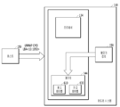
도 4는 본 발명의 실시 예에 따른 메모리 시스템에서 메모리 장치 구조를 개략적으로 도시한 도면이다.
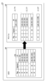
도 5a는 본 발명의 실시 예에 따른 제 1 테이블의 구조를 나타낸 도면이다.
도 5b는 본 발명의 실시 예에 따른 제 2 테이블의 구조를 나타낸 도면이다.
도 6a 내지 도 6e는 본 발명의 일 실시 예에 따른 메모리 시스템의 동작을 나타낸다.
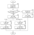
도 7은 본 발명의 실시 예에 따른 메모리 시스템의 동작 과정을 나타낸 흐름도이다.
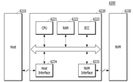
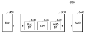
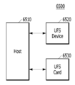
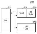
도 8 내지 도 16은 본 발명의 실시 예에 따른 메모리 시스템을 포함하는 데이터 처리 시스템의 다른 일 예들을 개략적으로 도시한 도면이다.
Claims (20)
- 언맵 커맨드를 처리하는 메모리 시스템에 있어서,
상기 언맵 커맨드에 대한 타겟 논리주소와 연관된 제 1 매핑 정보 및 제 2 매핑 정보를 저장하는 메모리 장치; 및
상기 제 1 매핑 정보 및 상기 제 2 매핑 정보를 상기 메모리 장치로부터 로드하고, 상기 타겟 논리주소에 대응하는 맵 데이터의 전체 크기를 소정의 임계 값과 비교하며, 상기 비교 결과에 기초하여 적어도 하나 이상의 상기 타겟 논리주소를 포함하는 복수의 타겟 논리그룹들 각각과 매핑된 복수의 맵 세그먼트들을 복수의 영역으로 구분하고, 상기 복수의 영역 중 어느 한 영역에 포함된 맵 세그먼트 각각에 대하여 언맵 동작을 수행하는 컨트롤러
를 포함하며,
상기 제 1 매핑 정보는 상기 복수의 맵 세그먼트와 상기 복수의 타겟 논리그룹들 각각의 매핑관계에 대한 정보이고, 상기 제 2 매핑 정보는 상기 타겟 논리주소와 물리주소간의 매핑관계에 대한 정보인
메모리 시스템.
- 제 1 항에 있어서,
상기 컨트롤러는
상기 제 1 매핑 정보 및 상기 제 2 매핑 정보를 저장하는 메모리;
상기 메모리 장치로부터 상기 제 1 매핑 정보 및 상기 제 2 매핑 정보를 상기 메모리로 로드하는 프로세서; 및
상기 맵 데이터의 전체 크기를 소정의 임계 값과 비교하고, 상기 비교 결과에 기초하여 상기 비교 결과에 기초하여 상기 복수의 타겟 논리그룹과 매핑된 상기 복수의 맵 세그먼트들을 복수의 영역으로 구분하고, 상기 복수의 영역 중 어느 한 영역에 포함된 맵 세그먼트 각각의 제 1 매핑 정보에 대하여 언맵 동작을 수행하는 언맵관리부
를 포함하는 메모리 시스템.
- 제 2 항에 있어서,
상기 언맵관리부는
상기 맵 데이터의 전체 크기가 소정의 임계 값보다 크거나 같은 경우, 상기 복수의 맵 세그먼트들 중 상기 복수의 타겟 논리그룹들에 포함된 복수의 논리주소들 중 일부만 상기 타겟 논리주소인 제 1 논리그룹과 매핑된 맵 세그먼트를 제 1 영역 및 제 3 영역으로 구분하고, 상기 복수의 타겟 논리그룹들에 포함된 복수의 논리주소들 중 전부 상기 타겟 논리주소인 제 2 논리그룹과 매핑된 맵 세그먼트를 제 2 영역으로 구분하는
메모리 시스템.
- 제 3 항에 있어서,
상기 언맵관리부는
상기 제 1 논리그룹 중 상기 타겟 논리주소의 시작 논리주소를 포함하는 논리그룹과 매핑된 맵 세그먼트를 제 1 영역으로 구분하고,
상기 제 1 논리그룹 중 상기 타겟 논리주소의 마지막 논리주소를 포함하는 논리그룹과 매핑된 맵 세그먼트를 제 3 영역으로 구분하는
메모리 시스템.
- 제 3 항에 있어서,
상기 제 2 영역에 포함된 맵 세그먼트 각각의 상기 제 1 매핑 정보에 대하여 제 1 언맵 동작을 수행하고,
상기 제 1 영역의 맵 세그먼트 및 상기 제 3 영역 각각의 맵 세그먼트 각각과 매핑된 논리그룹에 포함된 타겟 논리주소의 상기 제 2 매핑 정보에 대하여 제 2 언맵 동작을 수행하는
메모리 시스템.
- 제 5 항에 있어서,
상기 프로세서는
상기 제 1 언맵 동작이 수행된 후에, 상기 제 1 매핑 정보를 상기 메모리 장치에 저장하는
메모리 시스템.
- 제 5 항에 있어서,
상기 프로세서는
상기 제 2 언맵 동작이 수행된 후에, 상기 제 2 매핑 정보를 상기 메모리 장치에 저장하는
메모리 시스템.
- 제 2 항에 있어서,
상기 언맵관리부는
상기 맵 데이터의 전체 크기가 소정의 임계 값보다 작을 때, 상기 타겟 논리주소의 상기 제 2 매핑 정보에 대하여 제 3 언맵 동작을 수행하는
메모리 시스템.
- 제 8 항에 있어서,
상기 프로세서는
상기 제 3 언맵 동작이 수행된 후, 상기 제 2 매핑 정보를 상기 메모리 장치에 저장하는
메모리 시스템.
- 제 2 항에 있어서,
상기 메모리는
상기 제 1 매핑 정보가 기록된 제 1 테이블 및 상기 제 2 매핑 정보가 기록된 제 2 테이블을 저장하는
메모리 시스템.
- 언맵 커맨드를 처리하는 메모리 시스템의 동작방법에 있어서,
상기 언맵 커맨드를 제공받는 단계;
상기 언맵 커맨드에 대한 타겟 논리주소와 연관된 제 1 매핑 정보 및 제 2 매핑 정보를 메모리 장치로부터 리드하여 메모리에 저장하는 단계;
상기 타겟 논리주소에 대응하는 맵 데이터의 전체 크기와 소정의 임계 값을 비교하는 단계;
상기 비교 결과에 기초하여 적어도 하나 이상의 상기 타겟 논리주소를 포함하는 복수의 타겟 논리그룹들 각각과 매핑된 복수의 맵 세그먼트들에 대하여 복수의 영역을 구분하는 단계; 및
상기 복수의 영역 중 어느 한 영역에 포함된 맵 세그먼트 각각에 대하여 언맵 동작을 수행하는 단계
를 포함하고
상기 제 1 매핑 정보는 상기 복수의 맵 세그먼트와 상기 복수의 타겟 논리그룹들 각각의 매핑관계에 대한 정보이고, 상기 제 2 매핑 정보는 상기 타겟 논리주소와 물리주소간의 매핑관계에 대한 정보인
메모리 시스템의 동작방법.
- 제 11 항에 있어서,
상기 영역을 구분하는 단계는
상기 맵 데이터의 전체 크기가 소정의 임계 값보다 크거나 같은 경우, 상기 복수의 타겟 논리그룹들 각각과 매핑된 상기 복수의 맵 세그먼트들에 대하여 복수의 영역을 구분하는
메모리 시스템의 동작방법.
- 제 12 항에 있어서,
상기 영역을 구분하는 단계는
상기 복수의 맵 세그먼트들 중 상기 복수의 타겟 논리그룹들에 포함된 복수의 논리주소들 중 일부만 상기 타겟 논리주소인 제 1 논리그룹과 매핑된 맵 세그먼트를 제 1 영역 및 제 3 영역으로 구분하고, 상기 복수의 타겟 논리그룹들에 포함된 복수의 논리주소들 중 전부 상기 타겟 논리주소인 제 2 논리그룹과 매핑된 맵 세그먼트를 제 2 영역으로 구분하는
메모리 시스템의 동작방법.
- 제 13 항에 있어서,
상기 영역을 구분하는 단계는
상기 제 1 논리그룹 중 상기 타겟 논리주소의 시작 논리주소를 포함하는 논리그룹과 매핑된 맵 세그먼트를 제 1 영역으로 구분하고,
상기 제 1 논리그룹 중 상기 타겟 논리주소의 마지막 논리주소를 포함하는 논리그룹과 매핑된 맵 세그먼트를 제 3 영역으로 구분하는
메모리 시스템의 동작방법.
- 제 13 항에 있어서,
상기 언맵 동작을 수행하는 단계는
상기 제 2 영역에 포함된 맵 세그먼트 각각의 상기 제 1 매핑 정보에 대하여 제 1 언맵 동작을 수행하고,
상기 제 1 영역의 맵 세그먼트 및 상기 제 3 영역 각각의 맵 세그먼트 각각과 매핑된 논리그룹에 포함된 타겟 논리주소의 상기 제 2 매핑 정보에 대하여 제 2 언맵 동작을 수행하는
메모리 시스템의 동작방법.
- 제 15 항에 있어서,
상기 제 1 언맵 동작이 수행된 후에, 상기 제 1 매핑 정보를 상기 메모리 장치에 저장하는 단계
를 더 포함하는 메모리 시스템의 동작방법.
- 제 15 항에 있어서,
상기 제 2 언맵 동작이 수행된 후에, 상기 제 2 매핑 정보를 상기 메모리 장치에 저장하는 단계
를 더 포함하는 메모리 시스템의 동작방법.
- 제 11 항에 있어서,
상기 맵 데이터의 전체 크기가 소정의 임계 값보다 작을 때,
상기 언맵 동작을 수행하는 단계는
상기 타겟 논리주소의 상기 제 2 매핑 정보에 대하여 제 3 언맵 동작을 수행하는
메모리 시스템의 동작방법.
- 제 18 항에 있어서,
상기 제 3 언맵 동작이 수행된 후, 상기 제 2 매핑 정보를 상기 메모리 장치에 저장하는 단계
를 더 포함하는 메모리 시스템의 동작방법.
- 제 11 항에 있어서,
상기 제 1 매핑 정보가 기록된 제 1 테이블 및 상기 제 2 매핑 정보가 기록된 제 2 테이블을 상기 메모리에 저장하는 단계
를 더 포함하는 메모리 시스템.
Priority Applications (3)
| Application Number | Priority Date | Filing Date | Title |
|---|---|---|---|
| KR1020180163281A KR102761223B1 (ko) | 2018-12-17 | 2018-12-17 | 메모리 시스템 및 그것의 동작방법 |
| US16/684,037 US11016881B2 (en) | 2018-12-17 | 2019-11-14 | Memory system and operating method thereof |
| CN201911213480.9A CN111324552B (zh) | 2018-12-17 | 2019-12-02 | 存储器系统及其操作方法 |
Applications Claiming Priority (1)
| Application Number | Priority Date | Filing Date | Title |
|---|---|---|---|
| KR1020180163281A KR102761223B1 (ko) | 2018-12-17 | 2018-12-17 | 메모리 시스템 및 그것의 동작방법 |
Publications (2)
| Publication Number | Publication Date |
|---|---|
| KR20200074647A true KR20200074647A (ko) | 2020-06-25 |
| KR102761223B1 KR102761223B1 (ko) | 2025-02-03 |
Family
ID=71072566
Family Applications (1)
| Application Number | Title | Priority Date | Filing Date |
|---|---|---|---|
| KR1020180163281A Active KR102761223B1 (ko) | 2018-12-17 | 2018-12-17 | 메모리 시스템 및 그것의 동작방법 |
Country Status (3)
| Country | Link |
|---|---|
| US (1) | US11016881B2 (ko) |
| KR (1) | KR102761223B1 (ko) |
| CN (1) | CN111324552B (ko) |
Families Citing this family (8)
| Publication number | Priority date | Publication date | Assignee | Title |
|---|---|---|---|---|
| US11733918B2 (en) * | 2020-07-28 | 2023-08-22 | Samsung Electronics Co., Ltd. | Systems and methods for processing commands for storage devices |
| US11755490B2 (en) * | 2020-12-15 | 2023-09-12 | Micron Technology, Inc. | Unmap operation techniques |
| US20230013048A1 (en) * | 2021-07-16 | 2023-01-19 | International Business Machines Corporation | Handling partition data |
| US11711488B2 (en) * | 2021-08-31 | 2023-07-25 | Micron Technology, Inc. | Configurable storage granularity for video/image recording |
| CN115904226B (zh) | 2022-10-10 | 2025-10-28 | 阿里巴巴(中国)有限公司 | 固态驱动器、设备及固态驱动器的操作方法 |
| CN119585704A (zh) | 2023-05-31 | 2025-03-07 | 长江存储科技有限责任公司 | 存储器系统及其操作方法、存储介质、存储器控制器 |
| CN117234959A (zh) * | 2023-08-29 | 2023-12-15 | 中电云计算技术有限公司 | 一种数据处理方法、装置、设备及存储介质 |
| CN117891416B (zh) * | 2024-03-18 | 2024-05-14 | 厦门大学 | 基于scsi协议的取消映射操作优化方法、装置及可读介质 |
Citations (2)
| Publication number | Priority date | Publication date | Assignee | Title |
|---|---|---|---|---|
| US20070234002A1 (en) * | 2006-04-04 | 2007-10-04 | Litke Adam G | Method and apparatus for temporary mapping of executable program segments |
| WO2016069188A1 (en) * | 2014-10-27 | 2016-05-06 | Sandisk Enterprise Ip Llc | Processing of un-map commands to enhance performance and endurance of a storage device |
Family Cites Families (16)
| Publication number | Priority date | Publication date | Assignee | Title |
|---|---|---|---|---|
| US4758951A (en) * | 1985-04-09 | 1988-07-19 | Tektronix, Inc. | Method for translating virtual addresses into real addresses |
| US8417912B2 (en) * | 2010-09-03 | 2013-04-09 | International Business Machines Corporation | Management of low-paging space conditions in an operating system |
| US9069657B2 (en) | 2011-12-12 | 2015-06-30 | Apple Inc. | LBA bitmap usage |
| US9323667B2 (en) | 2012-04-12 | 2016-04-26 | Violin Memory Inc. | System and method for managing trim operations in a flash memory system using mapping tables and block status tables |
| WO2015048140A1 (en) * | 2013-09-24 | 2015-04-02 | Intelligent Intellectual Property Holdings 2 Llc | Systems and methods for storage collision management |
| KR102793137B1 (ko) * | 2016-11-07 | 2025-04-10 | 삼성전자주식회사 | 어드레스 맵핑 테이블의 에러 정정을 수행하는 메모리 시스템 |
| JP2018116329A (ja) * | 2017-01-16 | 2018-07-26 | 富士通株式会社 | ストレージ制御装置、およびストレージ制御プログラム |
| US10459636B2 (en) * | 2017-03-24 | 2019-10-29 | Sandisk Technologies Llc | System and method for managing data in non-volatile memory systems having multiple mapping layers |
| US10275170B2 (en) * | 2017-04-10 | 2019-04-30 | Sandisk Technologies Llc | Folding operations in memory systems with single address updates |
| CN107220184B (zh) * | 2017-05-10 | 2019-07-09 | 杭州宏杉科技股份有限公司 | 一种lun存储单元的管理方法及装置 |
| US11182106B2 (en) * | 2018-03-21 | 2021-11-23 | Arm Limited | Refresh circuit for use with integrated circuits |
| KR20200019430A (ko) * | 2018-08-14 | 2020-02-24 | 에스케이하이닉스 주식회사 | 컨트롤러 및 그것의 동작방법 |
| US10909030B2 (en) * | 2018-09-11 | 2021-02-02 | Toshiba Memory Corporation | Enhanced trim command support for solid state drives |
| KR102679967B1 (ko) * | 2018-09-12 | 2024-07-02 | 에스케이하이닉스 주식회사 | 메모리 시스템에서의 유효 데이터 관리 방법 및 장치 |
| KR102711044B1 (ko) * | 2018-09-20 | 2024-09-27 | 에스케이하이닉스 주식회사 | 메모리 시스템에서의 유효 데이터 체크 방법 및 장치 |
| US10901649B2 (en) * | 2019-01-23 | 2021-01-26 | Vmware, Inc. | Storage reclamation for distributed storage systems |
-
2018
- 2018-12-17 KR KR1020180163281A patent/KR102761223B1/ko active Active
-
2019
- 2019-11-14 US US16/684,037 patent/US11016881B2/en active Active
- 2019-12-02 CN CN201911213480.9A patent/CN111324552B/zh active Active
Patent Citations (2)
| Publication number | Priority date | Publication date | Assignee | Title |
|---|---|---|---|---|
| US20070234002A1 (en) * | 2006-04-04 | 2007-10-04 | Litke Adam G | Method and apparatus for temporary mapping of executable program segments |
| WO2016069188A1 (en) * | 2014-10-27 | 2016-05-06 | Sandisk Enterprise Ip Llc | Processing of un-map commands to enhance performance and endurance of a storage device |
Also Published As
| Publication number | Publication date |
|---|---|
| KR102761223B1 (ko) | 2025-02-03 |
| CN111324552B (zh) | 2023-03-03 |
| US11016881B2 (en) | 2021-05-25 |
| CN111324552A (zh) | 2020-06-23 |
| US20200192792A1 (en) | 2020-06-18 |
Similar Documents
| Publication | Publication Date | Title |
|---|---|---|
| KR102694483B1 (ko) | 컨트롤러 및 그것의 동작방법 | |
| KR102761223B1 (ko) | 메모리 시스템 및 그것의 동작방법 | |
| KR102532563B1 (ko) | 메모리 장치 및 그것의 동작방법 | |
| KR20190044798A (ko) | 컨트롤러 및 컨트롤러의 동작방법 | |
| KR102737416B1 (ko) | 메모리 시스템 및 그것의 동작방법 | |
| KR20180079584A (ko) | 컨트롤러 및 컨트롤러의 동작 방법 | |
| KR20190113436A (ko) | 컨트롤러, 그것의 동작방법 및 컨트롤러를 포함하는 메모리 시스템 | |
| KR102748625B1 (ko) | 메모리 시스템 및 그것의 동작방법 | |
| KR20190138419A (ko) | 메모리 시스템 및 그것의 동작방법 | |
| KR20200019430A (ko) | 컨트롤러 및 그것의 동작방법 | |
| KR20200006379A (ko) | 컨트롤러 및 그것의 동작방법 | |
| KR102725203B1 (ko) | 데이터 처리 시스템 및 그의 동작방법 | |
| KR102586786B1 (ko) | 메모리 시스템 및 그것의 동작방법 | |
| KR102567314B1 (ko) | 메모리 시스템 및 그것의 동작방법 | |
| KR20200006378A (ko) | 컨트롤러 및 그것의 동작방법 | |
| KR102520412B1 (ko) | 메모리 시스템 및 그것의 동작방법 | |
| KR102730162B1 (ko) | 메모리 시스템 및 그것의 동작방법 | |
| KR102697321B1 (ko) | 메모리 시스템 및 그것의 동작방법 | |
| KR102513498B1 (ko) | 컨트롤러, 그것의 동작방법 및 컨트롤러를 포함하는 메모리 시스템 | |
| KR20190082513A (ko) | 컨트롤러 및 그것의 동작방법 | |
| KR102741401B1 (ko) | 데이터 처리 시스템 및 그것의 동작방법 | |
| KR102704708B1 (ko) | 메모리 시스템 및 그것의 동작방법 | |
| KR102689927B1 (ko) | 메모리 시스템 및 그것의 동작방법 | |
| KR102687593B1 (ko) | 컨트롤러 및 그것의 동작방법 | |
| KR102410296B1 (ko) | 컨트롤러 및 컨트롤러의 동작방법 |
Legal Events
| Date | Code | Title | Description |
|---|---|---|---|
| PA0109 | Patent application |
Patent event code: PA01091R01D Comment text: Patent Application Patent event date: 20181217 |
|
| PG1501 | Laying open of application | ||
| A201 | Request for examination | ||
| PA0201 | Request for examination |
Patent event code: PA02012R01D Patent event date: 20211209 Comment text: Request for Examination of Application Patent event code: PA02011R01I Patent event date: 20181217 Comment text: Patent Application |
|
| E902 | Notification of reason for refusal | ||
| PE0902 | Notice of grounds for rejection |
Comment text: Notification of reason for refusal Patent event date: 20240827 Patent event code: PE09021S01D |
|
| E701 | Decision to grant or registration of patent right | ||
| PE0701 | Decision of registration |
Patent event code: PE07011S01D Comment text: Decision to Grant Registration Patent event date: 20241102 |
|
| GRNT | Written decision to grant | ||
| PR0701 | Registration of establishment |
Comment text: Registration of Establishment Patent event date: 20250123 Patent event code: PR07011E01D |
|
| PR1002 | Payment of registration fee |
Payment date: 20250124 End annual number: 3 Start annual number: 1 |
|
| PG1601 | Publication of registration |