KR20200076302A - 표시 패널 및 표시 장치 - Google Patents
표시 패널 및 표시 장치 Download PDFInfo
- Publication number
- KR20200076302A KR20200076302A KR1020180165270A KR20180165270A KR20200076302A KR 20200076302 A KR20200076302 A KR 20200076302A KR 1020180165270 A KR1020180165270 A KR 1020180165270A KR 20180165270 A KR20180165270 A KR 20180165270A KR 20200076302 A KR20200076302 A KR 20200076302A
- Authority
- KR
- South Korea
- Prior art keywords
- transistor
- plate
- disposed
- layer stack
- display panel
- Prior art date
- Legal status (The legal status is an assumption and is not a legal conclusion. Google has not performed a legal analysis and makes no representation as to the accuracy of the status listed.)
- Granted
Links
Images







Classifications
-
- G—PHYSICS
- G09—EDUCATION; CRYPTOGRAPHY; DISPLAY; ADVERTISING; SEALS
- G09G—ARRANGEMENTS OR CIRCUITS FOR CONTROL OF INDICATING DEVICES USING STATIC MEANS TO PRESENT VARIABLE INFORMATION
- G09G3/00—Control arrangements or circuits, of interest only in connection with visual indicators other than cathode-ray tubes
- G09G3/20—Control arrangements or circuits, of interest only in connection with visual indicators other than cathode-ray tubes for presentation of an assembly of a number of characters, e.g. a page, by composing the assembly by combination of individual elements arranged in a matrix no fixed position being assigned to or needed to be assigned to the individual characters or partial characters
- G09G3/22—Control arrangements or circuits, of interest only in connection with visual indicators other than cathode-ray tubes for presentation of an assembly of a number of characters, e.g. a page, by composing the assembly by combination of individual elements arranged in a matrix no fixed position being assigned to or needed to be assigned to the individual characters or partial characters using controlled light sources
- G09G3/30—Control arrangements or circuits, of interest only in connection with visual indicators other than cathode-ray tubes for presentation of an assembly of a number of characters, e.g. a page, by composing the assembly by combination of individual elements arranged in a matrix no fixed position being assigned to or needed to be assigned to the individual characters or partial characters using controlled light sources using electroluminescent panels
- G09G3/32—Control arrangements or circuits, of interest only in connection with visual indicators other than cathode-ray tubes for presentation of an assembly of a number of characters, e.g. a page, by composing the assembly by combination of individual elements arranged in a matrix no fixed position being assigned to or needed to be assigned to the individual characters or partial characters using controlled light sources using electroluminescent panels semiconductive, e.g. using light-emitting diodes [LED]
- G09G3/3208—Control arrangements or circuits, of interest only in connection with visual indicators other than cathode-ray tubes for presentation of an assembly of a number of characters, e.g. a page, by composing the assembly by combination of individual elements arranged in a matrix no fixed position being assigned to or needed to be assigned to the individual characters or partial characters using controlled light sources using electroluminescent panels semiconductive, e.g. using light-emitting diodes [LED] organic, e.g. using organic light-emitting diodes [OLED]
- G09G3/3266—Details of drivers for scan electrodes
-
- G—PHYSICS
- G02—OPTICS
- G02F—OPTICAL DEVICES OR ARRANGEMENTS FOR THE CONTROL OF LIGHT BY MODIFICATION OF THE OPTICAL PROPERTIES OF THE MEDIA OF THE ELEMENTS INVOLVED THEREIN; NON-LINEAR OPTICS; FREQUENCY-CHANGING OF LIGHT; OPTICAL LOGIC ELEMENTS; OPTICAL ANALOGUE/DIGITAL CONVERTERS
- G02F1/00—Devices or arrangements for the control of the intensity, colour, phase, polarisation or direction of light arriving from an independent light source, e.g. switching, gating or modulating; Non-linear optics
- G02F1/01—Devices or arrangements for the control of the intensity, colour, phase, polarisation or direction of light arriving from an independent light source, e.g. switching, gating or modulating; Non-linear optics for the control of the intensity, phase, polarisation or colour
- G02F1/13—Devices or arrangements for the control of the intensity, colour, phase, polarisation or direction of light arriving from an independent light source, e.g. switching, gating or modulating; Non-linear optics for the control of the intensity, phase, polarisation or colour based on liquid crystals, e.g. single liquid crystal display cells
- G02F1/133—Constructional arrangements; Operation of liquid crystal cells; Circuit arrangements
- G02F1/1333—Constructional arrangements; Manufacturing methods
-
- G—PHYSICS
- G02—OPTICS
- G02F—OPTICAL DEVICES OR ARRANGEMENTS FOR THE CONTROL OF LIGHT BY MODIFICATION OF THE OPTICAL PROPERTIES OF THE MEDIA OF THE ELEMENTS INVOLVED THEREIN; NON-LINEAR OPTICS; FREQUENCY-CHANGING OF LIGHT; OPTICAL LOGIC ELEMENTS; OPTICAL ANALOGUE/DIGITAL CONVERTERS
- G02F1/00—Devices or arrangements for the control of the intensity, colour, phase, polarisation or direction of light arriving from an independent light source, e.g. switching, gating or modulating; Non-linear optics
- G02F1/01—Devices or arrangements for the control of the intensity, colour, phase, polarisation or direction of light arriving from an independent light source, e.g. switching, gating or modulating; Non-linear optics for the control of the intensity, phase, polarisation or colour
- G02F1/13—Devices or arrangements for the control of the intensity, colour, phase, polarisation or direction of light arriving from an independent light source, e.g. switching, gating or modulating; Non-linear optics for the control of the intensity, phase, polarisation or colour based on liquid crystals, e.g. single liquid crystal display cells
- G02F1/133—Constructional arrangements; Operation of liquid crystal cells; Circuit arrangements
- G02F1/1333—Constructional arrangements; Manufacturing methods
- G02F1/1345—Conductors connecting electrodes to cell terminals
- G02F1/13452—Conductors connecting driver circuitry and terminals of panels
-
- G—PHYSICS
- G09—EDUCATION; CRYPTOGRAPHY; DISPLAY; ADVERTISING; SEALS
- G09G—ARRANGEMENTS OR CIRCUITS FOR CONTROL OF INDICATING DEVICES USING STATIC MEANS TO PRESENT VARIABLE INFORMATION
- G09G3/00—Control arrangements or circuits, of interest only in connection with visual indicators other than cathode-ray tubes
- G09G3/20—Control arrangements or circuits, of interest only in connection with visual indicators other than cathode-ray tubes for presentation of an assembly of a number of characters, e.g. a page, by composing the assembly by combination of individual elements arranged in a matrix no fixed position being assigned to or needed to be assigned to the individual characters or partial characters
- G09G3/34—Control arrangements or circuits, of interest only in connection with visual indicators other than cathode-ray tubes for presentation of an assembly of a number of characters, e.g. a page, by composing the assembly by combination of individual elements arranged in a matrix no fixed position being assigned to or needed to be assigned to the individual characters or partial characters by control of light from an independent source
- G09G3/36—Control arrangements or circuits, of interest only in connection with visual indicators other than cathode-ray tubes for presentation of an assembly of a number of characters, e.g. a page, by composing the assembly by combination of individual elements arranged in a matrix no fixed position being assigned to or needed to be assigned to the individual characters or partial characters by control of light from an independent source using liquid crystals
- G09G3/3611—Control of matrices with row and column drivers
- G09G3/3648—Control of matrices with row and column drivers using an active matrix
-
- G—PHYSICS
- G02—OPTICS
- G02F—OPTICAL DEVICES OR ARRANGEMENTS FOR THE CONTROL OF LIGHT BY MODIFICATION OF THE OPTICAL PROPERTIES OF THE MEDIA OF THE ELEMENTS INVOLVED THEREIN; NON-LINEAR OPTICS; FREQUENCY-CHANGING OF LIGHT; OPTICAL LOGIC ELEMENTS; OPTICAL ANALOGUE/DIGITAL CONVERTERS
- G02F1/00—Devices or arrangements for the control of the intensity, colour, phase, polarisation or direction of light arriving from an independent light source, e.g. switching, gating or modulating; Non-linear optics
- G02F1/01—Devices or arrangements for the control of the intensity, colour, phase, polarisation or direction of light arriving from an independent light source, e.g. switching, gating or modulating; Non-linear optics for the control of the intensity, phase, polarisation or colour
- G02F1/13—Devices or arrangements for the control of the intensity, colour, phase, polarisation or direction of light arriving from an independent light source, e.g. switching, gating or modulating; Non-linear optics for the control of the intensity, phase, polarisation or colour based on liquid crystals, e.g. single liquid crystal display cells
- G02F1/133—Constructional arrangements; Operation of liquid crystal cells; Circuit arrangements
- G02F1/136—Liquid crystal cells structurally associated with a semi-conducting layer or substrate, e.g. cells forming part of an integrated circuit
- G02F1/1362—Active matrix addressed cells
-
- G—PHYSICS
- G09—EDUCATION; CRYPTOGRAPHY; DISPLAY; ADVERTISING; SEALS
- G09F—DISPLAYING; ADVERTISING; SIGNS; LABELS OR NAME-PLATES; SEALS
- G09F9/00—Indicating arrangements for variable information in which the information is built-up on a support by selection or combination of individual elements
- G09F9/30—Indicating arrangements for variable information in which the information is built-up on a support by selection or combination of individual elements in which the desired character or characters are formed by combining individual elements
- G09F9/301—Indicating arrangements for variable information in which the information is built-up on a support by selection or combination of individual elements in which the desired character or characters are formed by combining individual elements flexible foldable or roll-able electronic displays, e.g. thin LCD, OLED
-
- G—PHYSICS
- G09—EDUCATION; CRYPTOGRAPHY; DISPLAY; ADVERTISING; SEALS
- G09F—DISPLAYING; ADVERTISING; SIGNS; LABELS OR NAME-PLATES; SEALS
- G09F9/00—Indicating arrangements for variable information in which the information is built-up on a support by selection or combination of individual elements
- G09F9/30—Indicating arrangements for variable information in which the information is built-up on a support by selection or combination of individual elements in which the desired character or characters are formed by combining individual elements
- G09F9/302—Indicating arrangements for variable information in which the information is built-up on a support by selection or combination of individual elements in which the desired character or characters are formed by combining individual elements characterised by the form or geometrical disposition of the individual elements
- G09F9/3026—Video wall, i.e. stackable semiconductor matrix display modules
-
- G—PHYSICS
- G09—EDUCATION; CRYPTOGRAPHY; DISPLAY; ADVERTISING; SEALS
- G09G—ARRANGEMENTS OR CIRCUITS FOR CONTROL OF INDICATING DEVICES USING STATIC MEANS TO PRESENT VARIABLE INFORMATION
- G09G3/00—Control arrangements or circuits, of interest only in connection with visual indicators other than cathode-ray tubes
- G09G3/20—Control arrangements or circuits, of interest only in connection with visual indicators other than cathode-ray tubes for presentation of an assembly of a number of characters, e.g. a page, by composing the assembly by combination of individual elements arranged in a matrix no fixed position being assigned to or needed to be assigned to the individual characters or partial characters
-
- G—PHYSICS
- G09—EDUCATION; CRYPTOGRAPHY; DISPLAY; ADVERTISING; SEALS
- G09G—ARRANGEMENTS OR CIRCUITS FOR CONTROL OF INDICATING DEVICES USING STATIC MEANS TO PRESENT VARIABLE INFORMATION
- G09G3/00—Control arrangements or circuits, of interest only in connection with visual indicators other than cathode-ray tubes
- G09G3/20—Control arrangements or circuits, of interest only in connection with visual indicators other than cathode-ray tubes for presentation of an assembly of a number of characters, e.g. a page, by composing the assembly by combination of individual elements arranged in a matrix no fixed position being assigned to or needed to be assigned to the individual characters or partial characters
- G09G3/22—Control arrangements or circuits, of interest only in connection with visual indicators other than cathode-ray tubes for presentation of an assembly of a number of characters, e.g. a page, by composing the assembly by combination of individual elements arranged in a matrix no fixed position being assigned to or needed to be assigned to the individual characters or partial characters using controlled light sources
- G09G3/30—Control arrangements or circuits, of interest only in connection with visual indicators other than cathode-ray tubes for presentation of an assembly of a number of characters, e.g. a page, by composing the assembly by combination of individual elements arranged in a matrix no fixed position being assigned to or needed to be assigned to the individual characters or partial characters using controlled light sources using electroluminescent panels
- G09G3/32—Control arrangements or circuits, of interest only in connection with visual indicators other than cathode-ray tubes for presentation of an assembly of a number of characters, e.g. a page, by composing the assembly by combination of individual elements arranged in a matrix no fixed position being assigned to or needed to be assigned to the individual characters or partial characters using controlled light sources using electroluminescent panels semiconductive, e.g. using light-emitting diodes [LED]
- G09G3/3208—Control arrangements or circuits, of interest only in connection with visual indicators other than cathode-ray tubes for presentation of an assembly of a number of characters, e.g. a page, by composing the assembly by combination of individual elements arranged in a matrix no fixed position being assigned to or needed to be assigned to the individual characters or partial characters using controlled light sources using electroluminescent panels semiconductive, e.g. using light-emitting diodes [LED] organic, e.g. using organic light-emitting diodes [OLED]
- G09G3/3225—Control arrangements or circuits, of interest only in connection with visual indicators other than cathode-ray tubes for presentation of an assembly of a number of characters, e.g. a page, by composing the assembly by combination of individual elements arranged in a matrix no fixed position being assigned to or needed to be assigned to the individual characters or partial characters using controlled light sources using electroluminescent panels semiconductive, e.g. using light-emitting diodes [LED] organic, e.g. using organic light-emitting diodes [OLED] using an active matrix
-
- G—PHYSICS
- G09—EDUCATION; CRYPTOGRAPHY; DISPLAY; ADVERTISING; SEALS
- G09G—ARRANGEMENTS OR CIRCUITS FOR CONTROL OF INDICATING DEVICES USING STATIC MEANS TO PRESENT VARIABLE INFORMATION
- G09G3/00—Control arrangements or circuits, of interest only in connection with visual indicators other than cathode-ray tubes
- G09G3/20—Control arrangements or circuits, of interest only in connection with visual indicators other than cathode-ray tubes for presentation of an assembly of a number of characters, e.g. a page, by composing the assembly by combination of individual elements arranged in a matrix no fixed position being assigned to or needed to be assigned to the individual characters or partial characters
- G09G3/22—Control arrangements or circuits, of interest only in connection with visual indicators other than cathode-ray tubes for presentation of an assembly of a number of characters, e.g. a page, by composing the assembly by combination of individual elements arranged in a matrix no fixed position being assigned to or needed to be assigned to the individual characters or partial characters using controlled light sources
- G09G3/30—Control arrangements or circuits, of interest only in connection with visual indicators other than cathode-ray tubes for presentation of an assembly of a number of characters, e.g. a page, by composing the assembly by combination of individual elements arranged in a matrix no fixed position being assigned to or needed to be assigned to the individual characters or partial characters using controlled light sources using electroluminescent panels
- G09G3/32—Control arrangements or circuits, of interest only in connection with visual indicators other than cathode-ray tubes for presentation of an assembly of a number of characters, e.g. a page, by composing the assembly by combination of individual elements arranged in a matrix no fixed position being assigned to or needed to be assigned to the individual characters or partial characters using controlled light sources using electroluminescent panels semiconductive, e.g. using light-emitting diodes [LED]
- G09G3/3208—Control arrangements or circuits, of interest only in connection with visual indicators other than cathode-ray tubes for presentation of an assembly of a number of characters, e.g. a page, by composing the assembly by combination of individual elements arranged in a matrix no fixed position being assigned to or needed to be assigned to the individual characters or partial characters using controlled light sources using electroluminescent panels semiconductive, e.g. using light-emitting diodes [LED] organic, e.g. using organic light-emitting diodes [OLED]
- G09G3/3225—Control arrangements or circuits, of interest only in connection with visual indicators other than cathode-ray tubes for presentation of an assembly of a number of characters, e.g. a page, by composing the assembly by combination of individual elements arranged in a matrix no fixed position being assigned to or needed to be assigned to the individual characters or partial characters using controlled light sources using electroluminescent panels semiconductive, e.g. using light-emitting diodes [LED] organic, e.g. using organic light-emitting diodes [OLED] using an active matrix
- G09G3/3233—Control arrangements or circuits, of interest only in connection with visual indicators other than cathode-ray tubes for presentation of an assembly of a number of characters, e.g. a page, by composing the assembly by combination of individual elements arranged in a matrix no fixed position being assigned to or needed to be assigned to the individual characters or partial characters using controlled light sources using electroluminescent panels semiconductive, e.g. using light-emitting diodes [LED] organic, e.g. using organic light-emitting diodes [OLED] using an active matrix with pixel circuitry controlling the current through the light-emitting element
-
- H01L27/32—
-
- H01L51/50—
-
- H—ELECTRICITY
- H10—SEMICONDUCTOR DEVICES; ELECTRIC SOLID-STATE DEVICES NOT OTHERWISE PROVIDED FOR
- H10D—INORGANIC ELECTRIC SEMICONDUCTOR DEVICES
- H10D86/00—Integrated devices formed in or on insulating or conducting substrates, e.g. formed in silicon-on-insulator [SOI] substrates or on stainless steel or glass substrates
- H10D86/40—Integrated devices formed in or on insulating or conducting substrates, e.g. formed in silicon-on-insulator [SOI] substrates or on stainless steel or glass substrates characterised by multiple TFTs
-
- H—ELECTRICITY
- H10—SEMICONDUCTOR DEVICES; ELECTRIC SOLID-STATE DEVICES NOT OTHERWISE PROVIDED FOR
- H10D—INORGANIC ELECTRIC SEMICONDUCTOR DEVICES
- H10D86/00—Integrated devices formed in or on insulating or conducting substrates, e.g. formed in silicon-on-insulator [SOI] substrates or on stainless steel or glass substrates
- H10D86/40—Integrated devices formed in or on insulating or conducting substrates, e.g. formed in silicon-on-insulator [SOI] substrates or on stainless steel or glass substrates characterised by multiple TFTs
- H10D86/441—Interconnections, e.g. scanning lines
-
- H—ELECTRICITY
- H10—SEMICONDUCTOR DEVICES; ELECTRIC SOLID-STATE DEVICES NOT OTHERWISE PROVIDED FOR
- H10D—INORGANIC ELECTRIC SEMICONDUCTOR DEVICES
- H10D86/00—Integrated devices formed in or on insulating or conducting substrates, e.g. formed in silicon-on-insulator [SOI] substrates or on stainless steel or glass substrates
- H10D86/40—Integrated devices formed in or on insulating or conducting substrates, e.g. formed in silicon-on-insulator [SOI] substrates or on stainless steel or glass substrates characterised by multiple TFTs
- H10D86/60—Integrated devices formed in or on insulating or conducting substrates, e.g. formed in silicon-on-insulator [SOI] substrates or on stainless steel or glass substrates characterised by multiple TFTs wherein the TFTs are in active matrices
-
- H—ELECTRICITY
- H10—SEMICONDUCTOR DEVICES; ELECTRIC SOLID-STATE DEVICES NOT OTHERWISE PROVIDED FOR
- H10K—ORGANIC ELECTRIC SOLID-STATE DEVICES
- H10K59/00—Integrated devices, or assemblies of multiple devices, comprising at least one organic light-emitting element covered by group H10K50/00
- H10K59/10—OLED displays
- H10K59/12—Active-matrix OLED [AMOLED] displays
- H10K59/123—Connection of the pixel electrodes to the thin film transistors [TFT]
-
- H—ELECTRICITY
- H10—SEMICONDUCTOR DEVICES; ELECTRIC SOLID-STATE DEVICES NOT OTHERWISE PROVIDED FOR
- H10K—ORGANIC ELECTRIC SOLID-STATE DEVICES
- H10K59/00—Integrated devices, or assemblies of multiple devices, comprising at least one organic light-emitting element covered by group H10K50/00
- H10K59/10—OLED displays
- H10K59/12—Active-matrix OLED [AMOLED] displays
- H10K59/124—Insulating layers formed between TFT elements and OLED elements
-
- H—ELECTRICITY
- H10—SEMICONDUCTOR DEVICES; ELECTRIC SOLID-STATE DEVICES NOT OTHERWISE PROVIDED FOR
- H10K—ORGANIC ELECTRIC SOLID-STATE DEVICES
- H10K59/00—Integrated devices, or assemblies of multiple devices, comprising at least one organic light-emitting element covered by group H10K50/00
- H10K59/10—OLED displays
- H10K59/12—Active-matrix OLED [AMOLED] displays
- H10K59/131—Interconnections, e.g. wiring lines or terminals
-
- H—ELECTRICITY
- H10—SEMICONDUCTOR DEVICES; ELECTRIC SOLID-STATE DEVICES NOT OTHERWISE PROVIDED FOR
- H10W—GENERIC PACKAGES, INTERCONNECTIONS, CONNECTORS OR OTHER CONSTRUCTIONAL DETAILS OF DEVICES COVERED BY CLASS H10
- H10W42/00—Arrangements for protection of devices
- H10W42/20—Arrangements for protection of devices protecting against electromagnetic or particle radiation, e.g. light, X-rays, gamma-rays or electrons
-
- H—ELECTRICITY
- H10—SEMICONDUCTOR DEVICES; ELECTRIC SOLID-STATE DEVICES NOT OTHERWISE PROVIDED FOR
- H10W—GENERIC PACKAGES, INTERCONNECTIONS, CONNECTORS OR OTHER CONSTRUCTIONAL DETAILS OF DEVICES COVERED BY CLASS H10
- H10W90/00—Package configurations
-
- G—PHYSICS
- G06—COMPUTING OR CALCULATING; COUNTING
- G06F—ELECTRIC DIGITAL DATA PROCESSING
- G06F3/00—Input arrangements for transferring data to be processed into a form capable of being handled by the computer; Output arrangements for transferring data from processing unit to output unit, e.g. interface arrangements
- G06F3/14—Digital output to display device ; Cooperation and interconnection of the display device with other functional units
- G06F3/1423—Digital output to display device ; Cooperation and interconnection of the display device with other functional units controlling a plurality of local displays, e.g. CRT and flat panel display
- G06F3/1446—Digital output to display device ; Cooperation and interconnection of the display device with other functional units controlling a plurality of local displays, e.g. CRT and flat panel display display composed of modules, e.g. video walls
-
- G—PHYSICS
- G09—EDUCATION; CRYPTOGRAPHY; DISPLAY; ADVERTISING; SEALS
- G09G—ARRANGEMENTS OR CIRCUITS FOR CONTROL OF INDICATING DEVICES USING STATIC MEANS TO PRESENT VARIABLE INFORMATION
- G09G2300/00—Aspects of the constitution of display devices
- G09G2300/02—Composition of display devices
- G09G2300/026—Video wall, i.e. juxtaposition of a plurality of screens to create a display screen of bigger dimensions
-
- G—PHYSICS
- G09—EDUCATION; CRYPTOGRAPHY; DISPLAY; ADVERTISING; SEALS
- G09G—ARRANGEMENTS OR CIRCUITS FOR CONTROL OF INDICATING DEVICES USING STATIC MEANS TO PRESENT VARIABLE INFORMATION
- G09G2300/00—Aspects of the constitution of display devices
- G09G2300/04—Structural and physical details of display devices
- G09G2300/0404—Matrix technologies
- G09G2300/0408—Integration of the drivers onto the display substrate
-
- G—PHYSICS
- G09—EDUCATION; CRYPTOGRAPHY; DISPLAY; ADVERTISING; SEALS
- G09G—ARRANGEMENTS OR CIRCUITS FOR CONTROL OF INDICATING DEVICES USING STATIC MEANS TO PRESENT VARIABLE INFORMATION
- G09G2300/00—Aspects of the constitution of display devices
- G09G2300/04—Structural and physical details of display devices
- G09G2300/0421—Structural details of the set of electrodes
- G09G2300/0426—Layout of electrodes and connections
-
- G—PHYSICS
- G09—EDUCATION; CRYPTOGRAPHY; DISPLAY; ADVERTISING; SEALS
- G09G—ARRANGEMENTS OR CIRCUITS FOR CONTROL OF INDICATING DEVICES USING STATIC MEANS TO PRESENT VARIABLE INFORMATION
- G09G3/00—Control arrangements or circuits, of interest only in connection with visual indicators other than cathode-ray tubes
- G09G3/03—Control arrangements or circuits, of interest only in connection with visual indicators other than cathode-ray tubes specially adapted for displays having non-planar surfaces, e.g. curved displays
- G09G3/035—Control arrangements or circuits, of interest only in connection with visual indicators other than cathode-ray tubes specially adapted for displays having non-planar surfaces, e.g. curved displays for flexible display surfaces
-
- H—ELECTRICITY
- H10—SEMICONDUCTOR DEVICES; ELECTRIC SOLID-STATE DEVICES NOT OTHERWISE PROVIDED FOR
- H10D—INORGANIC ELECTRIC SEMICONDUCTOR DEVICES
- H10D86/00—Integrated devices formed in or on insulating or conducting substrates, e.g. formed in silicon-on-insulator [SOI] substrates or on stainless steel or glass substrates
- H10D86/40—Integrated devices formed in or on insulating or conducting substrates, e.g. formed in silicon-on-insulator [SOI] substrates or on stainless steel or glass substrates characterised by multiple TFTs
- H10D86/421—Integrated devices formed in or on insulating or conducting substrates, e.g. formed in silicon-on-insulator [SOI] substrates or on stainless steel or glass substrates characterised by multiple TFTs having a particular composition, shape or crystalline structure of the active layer
- H10D86/423—Integrated devices formed in or on insulating or conducting substrates, e.g. formed in silicon-on-insulator [SOI] substrates or on stainless steel or glass substrates characterised by multiple TFTs having a particular composition, shape or crystalline structure of the active layer comprising semiconductor materials not belonging to the Group IV, e.g. InGaZnO
Landscapes
- Engineering & Computer Science (AREA)
- Physics & Mathematics (AREA)
- General Physics & Mathematics (AREA)
- Theoretical Computer Science (AREA)
- Microelectronics & Electronic Packaging (AREA)
- Computer Hardware Design (AREA)
- Nonlinear Science (AREA)
- Chemical & Material Sciences (AREA)
- Crystallography & Structural Chemistry (AREA)
- Optics & Photonics (AREA)
- Mathematical Physics (AREA)
- Multimedia (AREA)
- Devices For Indicating Variable Information By Combining Individual Elements (AREA)
- Electroluminescent Light Sources (AREA)
Abstract
Description
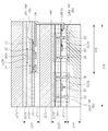
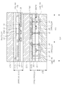
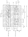
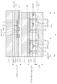
도 2 내지 도 4는 본 발명의 실시예들에 따른 표시 패널의 개략적인 단면 구조를 나타낸 도면들이다.
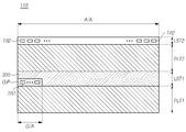
도 5는 본 발명의 실시예들에 따른 표시 패널의 액티브 영역과 게이트 구동 회로 영역을 나타낸 도면이다.
도 6은 본 발명의 실시예들에 따른 표시 패널에서, 제1 레이어 스택에서의 제1 금속과 제2 레이어 스택에서의 제2 금속을 전기적으로 연결해주기 위한 사이드 연결 구조를 나타낸 도면이다.
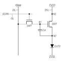
도 7은 본 발명의 실시예들에 따른 표시 패널의 서브픽셀 회로를 나타낸 도면이다.
도 8은 본 발명의 실시예들에 따른 표시 패널에 내장되는 게이트 구동 회로를 나타낸 도면이다.
도 9는 본 발명의 실시예들에 따른 표시 패널의 단면 구조를 나타낸 도면이다.
도 10 내지 도 12는 제1 레이어 스택에 포함된 제1 트랜지스터들과 제2 레이어 스택에 포함된 제2 트랜지스터들의 종류 별 단면 구조를 나타낸 도면들이다.
도 13은 본 발명의 실시예들에 따른 멀티 디스플레이를 나타낸 도면이다.
도 14는 도 13의 멀티 디스플레이의 응용 예를 나타낸 도면이다.
110: 표시 패널
120: 데이터 드라이버
130: 게이트 드라이버
140: 컨트롤러
PLT1, PLT2: 제1 플레이트, 제2 플레이트
LST1, LST2: 제1 레이어 스택, 제2 레이어 스택
TR1, TR2: 제1 트랜지스터, 제2 트랜지스터
GIP: 게이트 구동 회로
SRL: 사이드 라우팅 배선
M1, M2: 제1 금속, 제2 금속
BSM: 하부 쉴드 금속
Claims (15)
- 제1 플레이트;
상기 제1 플레이트 상에 위치하는 제2 플레이트;
상기 제1 플레이트과 상기 제2 플레이트 사이에 위치하며 제1 트랜지스터가 배치된 제1 레이어 스택; 및
상기 제2 플레이트 상에 위치하며 제2 트랜지스터가 배치되는 제2 레이어 스택을 포함하고,
상기 제1 트랜지스터는 영상 표시 영역에 해당하는 액티브 영역과 중첩되게 위치하는 표시 패널.
- 제1항에 있어서,
상기 제2 트랜지스터는 상기 액티브 영역에 배열되는 다수의 서브픽셀을 구성하는 트랜지스터이고,
상기 제1 트랜지스터는 상기 다수의 서브픽셀 중 하나 이상의 서브픽셀의 영역과 중첩되게 배치되는 표시 패널.
- 제2항에 있어서,
상기 제1 트랜지스터는,
상기 표시 패널에 내장되는 게이트 구동 회로에 포함되고, 상기 다수의 서브픽셀 중 외곽에 배치된 하나 이상의 서브픽셀의 영역과 중첩되게 배치되는 표시 패널.
- 제1항에 있어서,
상기 제1 레이어 스택에 위치하는 제1 금속과 상기 제2 레이어 스택에 위치하는 제2 금속을 전기적으로 연결해주는 사이드 라우팅 배선이 상기 제2 플레이트의 측면을 따라 배치되는 표시 패널.
- 제4항에 있어서,
상기 제1 금속은,
상기 제1 트랜지스터의 소스 전극 또는 드레인 전극이거나, 상기 제1 트랜지스터의 소스 전극 또는 드레인 전극과 전기적으로 연결된 패턴에 해당하고,
상기 제2 금속은,
상기 제2 트랜지스터의 게이트 전극과 전기적으로 연결된 게이트 라인이거나, 상기 게이트 라인에 전기적으로 연결된 패턴에 해당하는 표시 패널.
- 제1항에 있어서,
상기 제1 레이어 스택은 하나 이상의 무기 절연막을 포함하는 표시 패널.
- 제1항에 있어서,
상기 제1 트랜지스터는 상기 표시 패널에 내장되는 게이트 구동 회로에 포함되고,
상기 제1 트랜지스터의 하부에는 하부 쉴드 금속이 배치되고,
상기 하부 쉴드 금속은,
플로팅 되어 있거나, 상기 제1 트랜지스터의 소스 전극, 드레인 전극 및 게이트 전극 중 하나와 전기적으로 연결되는 표시 패널.
- 제1항에 있어서,
상기 제1 트랜지스터 및 상기 제2 트랜지스터는 다른 종류의 트랜지스터를 포함하는 표시 패널.
- 제8항에 있어서,
상기 제1 트랜지스터는 저온폴리실리콘 트랜지스터를 포함하고,
상기 제2 트랜지스터는 상기 산화물 트랜지스터를 포함하고,
상기 제2 플레이트는 폴리이미드 기판을 포함하는 표시 패널.
- 제1항에 있어서,
상기 제1 트랜지스터 및 상기 제2 트랜지스터는 동일한 종류의 트랜지스터를 포함하는 표시 패널.
- 제10항에 있어서,
상기 제1 트랜지스터 및 상기 제2 트랜지스터는 폴리실리콘 트랜지스터를 포함하고,
상기 제2 플레이트는 유기 절연막 또는 폴리이미드 기판을 포함하는 표시 패널. - 하나 이상의 표시 패널을 포함하는 표시부와,
상기 하나 이상의 표시 패널에 배치된 데이터 라인들을 구동하기 위한 데이터 구동 회로를 포함하고,
상기 하나 이상의 표시 패널 각각은,
제1 플레이트;
상기 제1 플레이트 상에 위치하는 제2 플레이트;
상기 제1 플레이트와 상기 제2 플레이트 사이에 위치하며 제1 트랜지스터가 배치된 제1 레이어 스택; 및
상기 제2 플레이트 상에 위치하며 제2 트랜지스터가 배치되는 제2 레이어 스택을 포함하고,
상기 제1 트랜지스터는 영상 표시 영역에 해당하는 액티브 영역과 중첩되게 위치하는 표시 장치.
- 제12항에 있어서,
상기 제2 트랜지스터는 상기 액티브 영역에 배열되는 다수의 서브픽셀을 구성하는 트랜지스터이고,
상기 제1 트랜지스터는 상기 다수의 서브픽셀 중 하나 이상의 서브픽셀의 영역과 중첩되게 배치되는 표시 장치.
- 제12항에 있어서,
상기 제1 트랜지스터는,
상기 다수의 표시 패널 각각에 내장되는 게이트 구동 회로에 포함되고, 상기 다수의 서브픽셀 중 외곽에 배치된 하나 이상의 서브픽셀의 영역과 중첩되게 배치되는 표시 장치.
- 제12항에 있어서,
상기 표시부는 둘 이상의 표시 패널을 포함하고, 원통 형상을 갖고,
상기 제1 플레이트 및 상기 제2 플레이트는 플렉서블 플레이트인 표시 장치.
Priority Applications (3)
| Application Number | Priority Date | Filing Date | Title |
|---|---|---|---|
| KR1020180165270A KR102612390B1 (ko) | 2018-12-19 | 2018-12-19 | 표시 패널 및 표시 장치 |
| CN201910644833.4A CN111341279B (zh) | 2018-12-19 | 2019-07-17 | 显示面板和显示装置 |
| US16/523,421 US11367399B2 (en) | 2018-12-19 | 2019-07-26 | Display panel and display device |
Applications Claiming Priority (1)
| Application Number | Priority Date | Filing Date | Title |
|---|---|---|---|
| KR1020180165270A KR102612390B1 (ko) | 2018-12-19 | 2018-12-19 | 표시 패널 및 표시 장치 |
Publications (2)
| Publication Number | Publication Date |
|---|---|
| KR20200076302A true KR20200076302A (ko) | 2020-06-29 |
| KR102612390B1 KR102612390B1 (ko) | 2023-12-12 |
Family
ID=71098864
Family Applications (1)
| Application Number | Title | Priority Date | Filing Date |
|---|---|---|---|
| KR1020180165270A Active KR102612390B1 (ko) | 2018-12-19 | 2018-12-19 | 표시 패널 및 표시 장치 |
Country Status (3)
| Country | Link |
|---|---|
| US (1) | US11367399B2 (ko) |
| KR (1) | KR102612390B1 (ko) |
| CN (1) | CN111341279B (ko) |
Cited By (2)
| Publication number | Priority date | Publication date | Assignee | Title |
|---|---|---|---|---|
| WO2024181653A1 (ko) * | 2023-03-02 | 2024-09-06 | 삼성전자주식회사 | 디스플레이 장치 |
| US12499828B2 (en) | 2021-07-16 | 2025-12-16 | Semiconductor Energy Laboratory Co., Ltd. | Electronic device |
Families Citing this family (13)
| Publication number | Priority date | Publication date | Assignee | Title |
|---|---|---|---|---|
| KR102805320B1 (ko) * | 2019-08-20 | 2025-05-13 | 삼성디스플레이 주식회사 | 표시 장치 및 그의 제조 방법 |
| CN115831972A (zh) * | 2020-12-31 | 2023-03-21 | 厦门天马微电子有限公司 | 显示面板及显示装置 |
| WO2022176772A1 (ja) * | 2021-02-18 | 2022-08-25 | ソニーセミコンダクタソリューションズ株式会社 | ディスプレイモジュールおよびその製造方法、ならびに電子機器 |
| KR20230050539A (ko) * | 2021-10-07 | 2023-04-17 | 삼성디스플레이 주식회사 | 표시 장치 |
| KR20240093706A (ko) * | 2021-10-22 | 2024-06-24 | 가부시키가이샤 한도오따이 에네루기 켄큐쇼 | 표시 장치 및 전자 기기 |
| KR20230069360A (ko) * | 2021-11-12 | 2023-05-19 | 엘지디스플레이 주식회사 | 표시장치 |
| KR102863273B1 (ko) * | 2021-12-27 | 2025-09-22 | 엘지디스플레이 주식회사 | 표시 장치 |
| KR20230108762A (ko) * | 2022-01-10 | 2023-07-19 | 삼성디스플레이 주식회사 | 표시 패널 및 이를 구비하는 표시 장치 |
| US20230378288A1 (en) * | 2022-05-20 | 2023-11-23 | Taiwan Semiconductor Manufacturing Company Ltd. | Semiconductor device and method of manufacturing semiconductor device |
| KR20240031491A (ko) * | 2022-08-30 | 2024-03-08 | 엘지디스플레이 주식회사 | 표시 패널 및 이를 포함하는 전계발광 표시장치 |
| KR20240119768A (ko) * | 2023-01-30 | 2024-08-06 | 엘지디스플레이 주식회사 | 표시 장치 |
| US20240260297A1 (en) * | 2023-01-31 | 2024-08-01 | Syndiant Inc. | Low profile pixel having electroluminescent devices and shared electrodes |
| WO2025233764A1 (ja) * | 2024-05-10 | 2025-11-13 | 株式会社半導体エネルギー研究所 | 表示装置 |
Citations (6)
| Publication number | Priority date | Publication date | Assignee | Title |
|---|---|---|---|---|
| JP2013222124A (ja) * | 2012-04-18 | 2013-10-28 | Sony Corp | 信号伝達装置、表示装置および電子機器 |
| JP2015194577A (ja) * | 2014-03-31 | 2015-11-05 | ソニー株式会社 | 表示装置および電子機器 |
| KR20170046683A (ko) * | 2014-08-30 | 2017-05-02 | 엘지디스플레이 주식회사 | 보강된 부분을 갖는 배선을 포함하는 플렉서블 디스플레이 디바이스 및 이의 제조 방법 |
| US20180012549A1 (en) * | 2016-07-05 | 2018-01-11 | Innolux Corporation | Display device |
| KR20180049226A (ko) * | 2014-08-31 | 2018-05-10 | 엘지디스플레이 주식회사 | 마이크로 커버층을 갖는 디스플레이 디바이스 및 이의 제조 방법 |
| KR20180133706A (ko) * | 2017-06-07 | 2018-12-17 | 엘지디스플레이 주식회사 | 터치 스크린을 갖는 유기 발광 표시 장치 및 이의 제조 방법 |
Family Cites Families (25)
| Publication number | Priority date | Publication date | Assignee | Title |
|---|---|---|---|---|
| JP4584144B2 (ja) * | 2003-01-22 | 2010-11-17 | 日本電気株式会社 | 回路基板装置及び配線基板間接続方法 |
| JP5014810B2 (ja) * | 2007-01-17 | 2012-08-29 | 株式会社ジャパンディスプレイイースト | 表示装置およびその製造方法 |
| KR101120924B1 (ko) * | 2007-03-20 | 2012-03-13 | 후지쯔 가부시끼가이샤 | 적층형 표시 소자 및 그 제조 방법 |
| WO2009128179A1 (ja) * | 2008-04-17 | 2009-10-22 | シャープ株式会社 | Tftアレイ基板、及び、液晶表示装置 |
| EP2525343A4 (en) * | 2010-01-13 | 2015-08-19 | Sharp Kk | MATRIX SUBSTRATE AND LIQUID CRYSTAL DISPLAY PANEL |
| TW201324760A (zh) * | 2011-12-07 | 2013-06-16 | Chunghwa Picture Tubes Ltd | 畫素結構及其製造方法 |
| KR102076666B1 (ko) * | 2013-04-11 | 2020-02-12 | 엘지디스플레이 주식회사 | 플렉서블 표시패널 |
| KR102159830B1 (ko) * | 2013-12-30 | 2020-09-24 | 엘지디스플레이 주식회사 | 표시소자 |
| KR101658716B1 (ko) * | 2014-12-31 | 2016-09-30 | 엘지디스플레이 주식회사 | 표시 장치 |
| KR102279021B1 (ko) * | 2015-05-27 | 2021-07-19 | 엘지디스플레이 주식회사 | 디스플레이 장치 |
| JP6663249B2 (ja) * | 2016-02-26 | 2020-03-11 | 株式会社ジャパンディスプレイ | 表示装置 |
| CN107579075B (zh) * | 2016-07-05 | 2020-11-27 | 群创光电股份有限公司 | 显示装置 |
| US10529745B2 (en) * | 2016-07-05 | 2020-01-07 | Innolux Corporation | Display device |
| CN106449706B (zh) * | 2016-10-17 | 2019-05-03 | 昆山国显光电有限公司 | 显示面板及其制造方法 |
| KR102702938B1 (ko) * | 2016-11-30 | 2024-09-03 | 엘지디스플레이 주식회사 | 멀티 타입의 박막 트랜지스터를 포함하는 유기발광 표시장치 |
| KR102793060B1 (ko) * | 2016-12-16 | 2025-04-08 | 엘지디스플레이 주식회사 | 표시 장치 및 그 제조 방법 |
| KR102687577B1 (ko) * | 2016-12-30 | 2024-07-22 | 엘지디스플레이 주식회사 | 발광 다이오드 표시 장치 및 이를 이용한 멀티 스크린 표시 장치 |
| WO2018172881A1 (ja) * | 2017-03-24 | 2018-09-27 | 株式会社半導体エネルギー研究所 | 半導体装置、表示システム及び電子機器 |
| CN107248521B (zh) * | 2017-06-19 | 2020-01-31 | 深圳市华星光电半导体显示技术有限公司 | Amoled背板结构 |
| KR20190010052A (ko) * | 2017-07-20 | 2019-01-30 | 엘지전자 주식회사 | 디스플레이 디바이스 |
| CN107623023A (zh) * | 2017-10-17 | 2018-01-23 | 京东方科技集团股份有限公司 | 一种oled显示面板及其制备方法、oled显示装置 |
| KR102413606B1 (ko) * | 2017-12-29 | 2022-06-24 | 엘지디스플레이 주식회사 | 구동 회로 내장형 표시패널 및 이를 이용한 영상 표시장치 |
| CN110349547A (zh) * | 2018-04-03 | 2019-10-18 | 群创光电股份有限公司 | 显示装置 |
| CN110556072B (zh) * | 2018-05-31 | 2024-07-02 | 三星电子株式会社 | 显示面板以及显示面板的驱动方法 |
| KR102538488B1 (ko) * | 2018-10-04 | 2023-06-01 | 삼성전자주식회사 | 디스플레이 패널 및 디스플레이 패널의 구동 방법 |
-
2018
- 2018-12-19 KR KR1020180165270A patent/KR102612390B1/ko active Active
-
2019
- 2019-07-17 CN CN201910644833.4A patent/CN111341279B/zh active Active
- 2019-07-26 US US16/523,421 patent/US11367399B2/en active Active
Patent Citations (6)
| Publication number | Priority date | Publication date | Assignee | Title |
|---|---|---|---|---|
| JP2013222124A (ja) * | 2012-04-18 | 2013-10-28 | Sony Corp | 信号伝達装置、表示装置および電子機器 |
| JP2015194577A (ja) * | 2014-03-31 | 2015-11-05 | ソニー株式会社 | 表示装置および電子機器 |
| KR20170046683A (ko) * | 2014-08-30 | 2017-05-02 | 엘지디스플레이 주식회사 | 보강된 부분을 갖는 배선을 포함하는 플렉서블 디스플레이 디바이스 및 이의 제조 방법 |
| KR20180049226A (ko) * | 2014-08-31 | 2018-05-10 | 엘지디스플레이 주식회사 | 마이크로 커버층을 갖는 디스플레이 디바이스 및 이의 제조 방법 |
| US20180012549A1 (en) * | 2016-07-05 | 2018-01-11 | Innolux Corporation | Display device |
| KR20180133706A (ko) * | 2017-06-07 | 2018-12-17 | 엘지디스플레이 주식회사 | 터치 스크린을 갖는 유기 발광 표시 장치 및 이의 제조 방법 |
Cited By (2)
| Publication number | Priority date | Publication date | Assignee | Title |
|---|---|---|---|---|
| US12499828B2 (en) | 2021-07-16 | 2025-12-16 | Semiconductor Energy Laboratory Co., Ltd. | Electronic device |
| WO2024181653A1 (ko) * | 2023-03-02 | 2024-09-06 | 삼성전자주식회사 | 디스플레이 장치 |
Also Published As
| Publication number | Publication date |
|---|---|
| US11367399B2 (en) | 2022-06-21 |
| US20200203382A1 (en) | 2020-06-25 |
| CN111341279B (zh) | 2022-05-03 |
| KR102612390B1 (ko) | 2023-12-12 |
| CN111341279A (zh) | 2020-06-26 |
Similar Documents
| Publication | Publication Date | Title |
|---|---|---|
| KR102612390B1 (ko) | 표시 패널 및 표시 장치 | |
| KR102727024B1 (ko) | 표시패널 및 표시장치 | |
| EP3637402B1 (en) | Display device | |
| TWI818705B (zh) | 顯示面板和包含該顯示面板的電子裝置 | |
| US11670239B2 (en) | Gate driving circuit and display device | |
| US11515425B2 (en) | Thin film transistor array substrate and electronic device including the same | |
| KR102520698B1 (ko) | Oled 표시패널 | |
| US12250850B2 (en) | Organic light emitting display device comprising multi type thin film transistor | |
| US12499812B2 (en) | Display device and display panel | |
| KR20200075318A (ko) | 박막 트랜지스터 및 디스플레이 패널 | |
| CN115662331A (zh) | 显示基板及其驱动方法、显示装置 | |
| US20240290797A1 (en) | Display Panel and Display Device | |
| KR102507763B1 (ko) | 표시장치 | |
| KR102930729B1 (ko) | 표시 패널 | |
| CN120236515A (zh) | 栅极驱动器和包括该栅极驱动器的显示装置 | |
| KR102551989B1 (ko) | 트랜지스터 및 전자장치 | |
| KR102937938B1 (ko) | 표시패널 및 이를 포함하는 표시장치 | |
| KR102603688B1 (ko) | 수직 구조 트랜지스터 및 전자장치 | |
| KR102486147B1 (ko) | 박막 트랜지스터 어레이 기판 및 이를 포함하는 전자장치 | |
| KR102563516B1 (ko) | 트랜지스터 및 전자장치 | |
| KR20170081073A (ko) | 표시 장치 및 그 제조 방법 | |
| KR20240107758A (ko) | 표시 장치 | |
| KR20230035203A (ko) | 표시패널과 이를 포함한 전자장치 |
Legal Events
| Date | Code | Title | Description |
|---|---|---|---|
| PA0109 | Patent application |
St.27 status event code: A-0-1-A10-A12-nap-PA0109 |
|
| PG1501 | Laying open of application |
St.27 status event code: A-1-1-Q10-Q12-nap-PG1501 |
|
| A201 | Request for examination | ||
| PA0201 | Request for examination |
St.27 status event code: A-1-2-D10-D11-exm-PA0201 |
|
| P22-X000 | Classification modified |
St.27 status event code: A-2-2-P10-P22-nap-X000 |
|
| P22-X000 | Classification modified |
St.27 status event code: A-2-2-P10-P22-nap-X000 |
|
| E902 | Notification of reason for refusal | ||
| PE0902 | Notice of grounds for rejection |
St.27 status event code: A-1-2-D10-D21-exm-PE0902 |
|
| P11-X000 | Amendment of application requested |
St.27 status event code: A-2-2-P10-P11-nap-X000 |
|
| P13-X000 | Application amended |
St.27 status event code: A-2-2-P10-P13-nap-X000 |
|
| E701 | Decision to grant or registration of patent right | ||
| PE0701 | Decision of registration |
St.27 status event code: A-1-2-D10-D22-exm-PE0701 |
|
| GRNT | Written decision to grant | ||
| PR0701 | Registration of establishment |
St.27 status event code: A-2-4-F10-F11-exm-PR0701 |
|
| PR1002 | Payment of registration fee |
St.27 status event code: A-2-2-U10-U11-oth-PR1002 Fee payment year number: 1 |
|
| PG1601 | Publication of registration |
St.27 status event code: A-4-4-Q10-Q13-nap-PG1601 |
|
| P22-X000 | Classification modified |
St.27 status event code: A-4-4-P10-P22-nap-X000 |