KR20200082012A - Touch type organic light emitting diode display device - Google Patents
Touch type organic light emitting diode display device Download PDFInfo
- Publication number
- KR20200082012A KR20200082012A KR1020180172125A KR20180172125A KR20200082012A KR 20200082012 A KR20200082012 A KR 20200082012A KR 1020180172125 A KR1020180172125 A KR 1020180172125A KR 20180172125 A KR20180172125 A KR 20180172125A KR 20200082012 A KR20200082012 A KR 20200082012A
- Authority
- KR
- South Korea
- Prior art keywords
- layer
- light emitting
- organic light
- emitting diode
- encapsulation layer
- Prior art date
- Legal status (The legal status is an assumption and is not a legal conclusion. Google has not performed a legal analysis and makes no representation as to the accuracy of the status listed.)
- Granted
Links
Images

Classifications
-
- G—PHYSICS
- G06—COMPUTING OR CALCULATING; COUNTING
- G06F—ELECTRIC DIGITAL DATA PROCESSING
- G06F3/00—Input arrangements for transferring data to be processed into a form capable of being handled by the computer; Output arrangements for transferring data from processing unit to output unit, e.g. interface arrangements
- G06F3/01—Input arrangements or combined input and output arrangements for interaction between user and computer
- G06F3/03—Arrangements for converting the position or the displacement of a member into a coded form
- G06F3/041—Digitisers, e.g. for touch screens or touch pads, characterised by the transducing means
- G06F3/0412—Digitisers structurally integrated in a display
-
- G—PHYSICS
- G06—COMPUTING OR CALCULATING; COUNTING
- G06F—ELECTRIC DIGITAL DATA PROCESSING
- G06F3/00—Input arrangements for transferring data to be processed into a form capable of being handled by the computer; Output arrangements for transferring data from processing unit to output unit, e.g. interface arrangements
- G06F3/01—Input arrangements or combined input and output arrangements for interaction between user and computer
- G06F3/03—Arrangements for converting the position or the displacement of a member into a coded form
- G06F3/041—Digitisers, e.g. for touch screens or touch pads, characterised by the transducing means
- G06F3/0416—Control or interface arrangements specially adapted for digitisers
-
- H01L27/323—
-
- H—ELECTRICITY
- H10—SEMICONDUCTOR DEVICES; ELECTRIC SOLID-STATE DEVICES NOT OTHERWISE PROVIDED FOR
- H10K—ORGANIC ELECTRIC SOLID-STATE DEVICES
- H10K59/00—Integrated devices, or assemblies of multiple devices, comprising at least one organic light-emitting element covered by group H10K50/00
- H10K59/40—OLEDs integrated with touch screens
-
- G—PHYSICS
- G06—COMPUTING OR CALCULATING; COUNTING
- G06F—ELECTRIC DIGITAL DATA PROCESSING
- G06F2203/00—Indexing scheme relating to G06F3/00 - G06F3/048
- G06F2203/041—Indexing scheme relating to G06F3/041 - G06F3/045
- G06F2203/04102—Flexible digitiser, i.e. constructional details for allowing the whole digitising part of a device to be flexed or rolled like a sheet of paper
Landscapes
- Engineering & Computer Science (AREA)
- General Engineering & Computer Science (AREA)
- Theoretical Computer Science (AREA)
- Human Computer Interaction (AREA)
- Physics & Mathematics (AREA)
- General Physics & Mathematics (AREA)
- Electroluminescent Light Sources (AREA)
Abstract
본 발명의 목적은, 터치입력을 처리할 수 있고, 표시장치의 두께와 베젤영역의 크기를 줄여 플렉서블 표시장치로 이용하는데 적합한 구조를 가지는 유기발광 다이오드 표시장치를 제공하는 것이다.
이를 위하여 본 발명은, 제 1 기판과; 상기 제 1 기판 상에 형성되는 박막 트랜지스터와; 상기 박막 트랜지스터를 덮는 보호층과; 상기 보호층 상에 형성되는 봉지층을 포함하고, 상기 봉지층에는 상기 보호층의 일부를 노출시키는 봉지층 컨택홀이 형성되고, 상기 보호층이 노출된 영역의 상부에는 터치전극이 형성되며, 상기 터치전극은 상기 박막 트랜지스터의 드레인 전극 또는 상기 제 1 기판 상에 형성되는 제 1 라인과 연결되는 유기발광 다이오드 표시장치를 제공한다.An object of the present invention is to provide an organic light emitting diode display device having a structure suitable for use as a flexible display device capable of processing a touch input and reducing the thickness of the display device and the size of the bezel area.
To this end, the present invention includes a first substrate; A thin film transistor formed on the first substrate; A protective layer covering the thin film transistor; It includes an encapsulation layer formed on the protective layer, an encapsulation layer contact hole exposing a part of the protective layer is formed in the encapsulation layer, and a touch electrode is formed on an upper portion of the region where the protective layer is exposed. The touch electrode provides an organic light emitting diode display connected to a drain electrode of the thin film transistor or a first line formed on the first substrate.
Description
본 발명은 유기발광 다이오드 표시장치에 관한 것으로, 특히 터치 입력을 처리할 수 있고 플렉서블 표시장치로 이용할 수 있는 유기발광 다이오드 표시장치에 관한 것이다.The present invention relates to an organic light emitting diode display, and more particularly, to an organic light emitting diode display that can process a touch input and can be used as a flexible display.
최근의 표시장치는 기존의 브라운관과 대비하여 얇고, 가벼우며, 소비전력이 작은 장점을 가진, 액정표시장치, 유기발광 다이오드 표시장치와 같은 평판 표시장치가 주류를 이루고 있다.In recent years, flat panel display devices such as liquid crystal display devices and organic light emitting diode display devices, which are thinner, lighter, and have lower power consumption than the conventional CRT, have become mainstream.
평판 표시장치 중에서 현재 주목되고 있는 유기발광 다이오드 표시장치는 자발광 특성을 가지는 유기발광 다이오드를 이용하여 화상을 표시한다. 유기발광 다이오드는 정공주입 전극과 유기 발광층, 전자주입 전극으로 이루어지며, 전자와 정공이 유기발광층 내부에서 결합하여 엑시톤(exciton)을 생성하고, 엑시톤이 여기 상태로부터 기저 상태로 떨어질 때 발생하는 에너지에 의해 빛이 발광하게 된다.Among the flat panel display devices, an organic light emitting diode display device that is currently attracting attention displays an image using an organic light emitting diode having self-luminous properties. The organic light emitting diode is composed of a hole injection electrode, an organic light emitting layer, and an electron injection electrode, and electrons and holes are combined inside the organic light emitting layer to generate excitons, and to the energy generated when the excitons fall from the excited state to the ground state. Light is emitted.
이렇게 유기발광 다이오드 표시장치는 자체적으로 발광할 수 있는 유기발광 다이오드를 포함하기 때문에, 백라이트를 필요로 하지 않아 가볍고 얇게 제조할 수 있다. 특히 유기발광 다이오드 표시패널의 기판을 유연성이 있는 소재로 형성하면, 이를 이용하여 평판 표시장치 뿐만 아니라 플렉서블(flexible) 표시장치를 구현할 수 있다.Since the organic light emitting diode display includes an organic light emitting diode capable of emitting light on its own, it is possible to manufacture lightly and thinly without requiring a backlight. In particular, when the substrate of the organic light emitting diode display panel is formed of a flexible material, a flexible display device as well as a flat panel display device can be realized using the substrate.
한편, 영상표시장치의 화면을 사람의 손 또는 물체로 선택하여 사용자의 명령을 입력할 수 있는 터치 타입의 표시장치가 널리 이용되고 있다.Meanwhile, a touch type display device that can select a screen of a video display device as a human hand or an object and input a user's command has been widely used.
터치 타입의 표시장치는 구조에 따라 터치스크린 부착형 방식(add-on type), 터치스크린 상판형 방식(on-cell type), 터치스크린 일체형 방식(in-cell type)으로 나눌 수 있다. 이중에서 터치스크린 부착형 방식은 표시패널과 터치패널을 개별적으로 제조한 후에 표시패널의 상부에 터치패널을 부착하는 방식이다. 그리고 터치스크린 상판형 방식은 표시패널의 상부 기판의 표면에 터치패널을 구성하는 소자들을 직접 형성하는 방식이다. 마지막으로 터치스크린 일체형 방식은 표시패널의 내부에 터치패널을 내장하는 방식으로, 표시장치의 두께가 얇아지고, 외부 빛에 의한 표면 반사가 줄어드는 장점이 있다.Depending on the structure, the touch type display device can be divided into an add-on type touch screen, an on-cell type touch screen, and an in-cell type touch screen. Among them, the touch screen attaching type is a method in which a touch panel is attached to an upper portion of the display panel after separately manufacturing the display panel and the touch panel. In addition, the touch screen top panel type is a method of directly forming elements constituting the touch panel on the surface of the upper substrate of the display panel. Lastly, the integrated touch screen method is a method of embedding a touch panel inside the display panel, and has a merit in that the thickness of the display device is reduced and surface reflection due to external light is reduced.
이와 같은 방식은 평판의 유기발광 다이오드 표시장치에 사용되어 터치 입력을 감지하고 처리할 수 있게 한다. 아울러 플렉서블 특성을 가지는 유기발광 다이오드 표시장치에서도 터치 입력을 감지할 수 있도록, 터치패널을 구성하는 소자를 형성하는 방식에 대한 연구가 진행되고 있다.Such a method is used in an organic light emitting diode display device of a flat panel to detect and process a touch input. In addition, research is being conducted on a method of forming an element constituting a touch panel so that a touch input can be detected even in an organic light emitting diode display device having flexible characteristics.
본 발명의 목적은, 터치입력을 처리할 수 있고, 표시장치의 두께와 베젤영역의 크기를 줄여 플렉서블 표시장치로 이용하는데 적합한 구조를 가지는 유기발광 다이오드 표시장치를 제공하는 것이다.An object of the present invention is to provide an organic light emitting diode display device having a structure suitable for use as a flexible display device capable of processing a touch input and reducing the thickness of the display device and the size of the bezel area.
상기와 같은 목적을 달성하기 위하여 본 발명은, 제 1 기판과; 상기 제 1 기판 상에 형성되는 박막 트랜지스터와; 상기 박막 트랜지스터를 덮는 보호층과; 상기 보호층 상에 형성되는 봉지층을 포함하고, 상기 봉지층에는 상기 보호층의 일부를 노출시키는 봉지층 컨택홀이 형성되고, 상기 보호층이 노출된 영역의 상부에는 터치전극이 형성되며, 상기 터치전극은 상기 박막 트랜지스터의 드레인 전극 또는 상기 제 1 기판 상에 형성되는 제 1 라인과 연결되는 유기발광 다이오드 표시장치를 제공한다.In order to achieve the above object, the present invention, the first substrate; A thin film transistor formed on the first substrate; A protective layer covering the thin film transistor; An encapsulation layer formed on the protective layer is included, an encapsulation layer contact hole exposing a part of the protection layer is formed in the encapsulation layer, and a touch electrode is formed on an upper portion of the region where the protection layer is exposed. The touch electrode provides an organic light emitting diode display connected to a drain electrode of the thin film transistor or a first line formed on the first substrate.
그리고, 상기 제 1 기판은 폴리이미드로 형성되는 유기발광 다이오드 표시장치를 제공한다.In addition, the first substrate provides an organic light emitting diode display formed of polyimide.
그리고, 상기 봉지층은 무기막층인 제 1 봉지층 및 제 2 봉지층과 유기막층을 포함하고, 상기 제 1 봉지층과 상기 제 2 봉지층 사이에는 유기막층이 형성되어 박막 봉지층을 이루는 유기발광 다이오드 표시장치를 제공한다.In addition, the encapsulation layer includes an inorganic layer, a first encapsulation layer, a second encapsulation layer, and an organic layer, and an organic light-emitting layer is formed between the first encapsulation layer and the second encapsulation layer to form an organic light-emitting layer. A diode display device is provided.
그리고, 상기 제 1 기판 상에 멀티 버퍼층과 액티브 버퍼층이 순차적으로 형성되고, 상기 액티브 버퍼층 상에 상기 박막 트랜지스터가 형성되며, 상기 박막 트랜지스터 상에 상기 보호층과 평탄화층이 순차적으로 형성되고, 상기 평탄화층 상에는 유기발광 다이오드와 이를 둘러싸는 뱅크가 형성되며, 상기 유기발광 다이오드와 상기 뱅크 상에는 상기 봉지층이 형성되고, 상기 봉지층 컨택홀은 상기 봉지층 및 상기 뱅크, 상기 평탄화층을 제거하여 상기 보호층의 일부를 노출시키는 유기발광 다이오드 표시장치를 제공한다.Then, a multi-buffer layer and an active buffer layer are sequentially formed on the first substrate, the thin film transistor is formed on the active buffer layer, the protective layer and a planarization layer are sequentially formed on the thin film transistor, and the planarization is performed. An organic light emitting diode and a bank surrounding it are formed on the layer, the encapsulation layer is formed on the organic light emitting diode and the bank, and the encapsulation layer contact hole removes the encapsulation layer, the bank, and the planarization layer to protect the An organic light emitting diode display device exposing a portion of a layer is provided.
그리고, 상기 보호층은 상기 박막 트랜지스터의 소스 전극 및 드레인 전극 상에 섬 형태로 형성되는 유기발광 다이오드 표시장를 제공한다.In addition, the protective layer provides an organic light emitting diode display formed in an island shape on the source electrode and the drain electrode of the thin film transistor.
그리고, 베젤영역이 아닌 비표시영역에 위치하는 터치패널 구동부를 포함하며, 상기 터치패널 구동부는 상기 제 1 라인을 통하여 터치입력 구동신호를 상기 터치전극으로 전송하고, 상기 터치전극은 상기 제 1 라인을 통하여 터치입력 감지신호를 상기 터치패널 구동부로 전송하는 유기발광 다이오드 표시장치를 제공한다. And, it includes a touch panel driver located in the non-display area, not the bezel area, the touch panel driver transmits a touch input driving signal to the touch electrode through the first line, and the touch electrode is the first line. It provides an organic light emitting diode display device for transmitting a touch input detection signal to the touch panel driver through.
그리고, 상기 제 1 라인은 데이터 라인인 유기발광 다이오드 표시장치를 제공한다.In addition, the first line provides an organic light emitting diode display device as a data line.
그리고, 상기 제 1 라인을 통해 상기 터치전극에 구동전원을 인가하는 유기발광 다이오드 표시장치를 제공한다.In addition, an organic light emitting diode display device that applies driving power to the touch electrode through the first line is provided.
이상 설명한 바와 같이 본 발명의 유기발광 다이오드 표시장치는, 봉지층에 보호층을 노출하는 컨택홀을 형성하고 터치전극을 컨택홀에 배치함으로써, 봉지층 상에 형성되는 터치패널을 제거할 수 있다. 이에 따라 유기발광 다이오드 표시패널의 두께를 줄이고 유연성을 증가시켜 터치 입력이 가능한 플렉서블 표시장치를 구현할 수 있다. 그리고 컨택홀에 배치된 터치전극을 어레이 기판 상에 형성되는 라인과 연결함으로써, 터치패널 구동회로인 Tx 구동부와 Rx 구동부를 베젤영역에서 제거할 수 있다. 이에 따라 베젤영역의 크기를 줄여 공간의 활용성을 높인 플렉서블 표시장치를 구현할 수 있다.As described above, the organic light emitting diode display device of the present invention can remove the touch panel formed on the encapsulation layer by forming a contact hole exposing the protective layer on the encapsulation layer and disposing the touch electrode in the contact hole. Accordingly, a flexible display device capable of a touch input may be realized by reducing the thickness of the organic light emitting diode display panel and increasing flexibility. In addition, the Tx driver and the Rx driver, which are the touch panel driving circuits, can be removed from the bezel area by connecting the touch electrode disposed in the contact hole to a line formed on the array substrate. Accordingly, it is possible to implement a flexible display device that increases the usability of the space by reducing the size of the bezel area.
도 1은 터치패널을 포함하는 유기발광 다이오드 표시패널의 단면을 나타낸 도면이다.
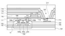
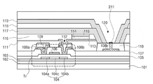
도 2a와 도 2b는 본 발명의 유기발광 다이오드 표시패널의 단면을 나타낸 도면이다.
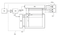
도 3은 본 발명의 유기발광 다이오드 표시장치의 전체 구성을 나타낸 도면이다.1 is a view showing a cross-section of an organic light emitting diode display panel including a touch panel.
2A and 2B are cross-sectional views of an organic light emitting diode display panel of the present invention.
3 is a view showing the overall configuration of the organic light emitting diode display device of the present invention.
이하, 도면을 참조하여 본 발명에 따른 실시 예를 상세하게 설명한다.Hereinafter, embodiments according to the present invention will be described in detail with reference to the drawings.
도 1은 터치패널을 포함하는 유기발광 다이오드 표시패널의 단면을 나타낸 도면이다.1 is a view showing a cross-section of an organic light emitting diode display panel including a touch panel.
유기발광 다이오드 표시패널은 표시패널(10)과 터치패널(20)을 포함한다. 제 1 기판(11) 상에는 소스 영역(12a) 및 드레인 영역(12b), 액티브 영역(12c)으로 구성된 반도체층(12)이 형성되고, 반도체층(12) 상에는 게이트 절연층(13)이 형성되며, 게이트 절연층(13) 상에는 게이트 전극(14)과 층간 절연층(15), 소스 전극(16a), 드레인 전극(16b)이 형성되어 박막 트랜지스터(Tr)를 이루게 된다.The organic light emitting diode display panel includes a
박막 트랜지스터(Tr) 상에는 보호층(17)과 유기발광 다이오드(E)가 차례대로 형성된다. 유기발광 다이오드(E)는 양의 전극(EA)과 유기발광층(EO), 음의 전극(EC)을 포함하며, 유기발광 다이오드(E)의 측면을 뱅크(18)가 둘러싸고 있다. 유기발광 다이오드(E) 상에는 유기막과 무기막이 다중층을 이루는 봉지층(19)이 형성되어 수분 등이 유기발광 다이오드(E)에 침투하는 것을 방지할 수 있다.The
봉지층(19) 상에는 터치전극(21)과, 터치입력 구동신호를 전송하는 Tx 라인(미도시), 터치입력 감지신호를 전송하는 Rx 라인(미도시), 터치전극에 전원을 인가하는 구동전원 라인(미도시)을 포함한 터치패널(20)이 형성되어, 표시장치 사용자의 터치입력을 처리할 수 있다.On the
그러나 봉지층(19) 상에 터치전극(21) 등을 포함한 터치패널(20)이 형성되므로 유기발광 다이오드 표시장치의 두께가 커질 수 있다. 굽힐 수 있는 형태(bendable), 말 수 있는 형태(rollable), 접을 수 있는 형태(foldable), 곡면 형태(curved) 등의 다양한 형태를 가지는 플렉서블 표시장치는 패널이 두꺼울수록 변형이 가능한 범위가 줄어들어 유연성이 떨어지게 된다.However, since the
그리고 Tx 라인에 터치입력 구동신호를 전송하고, Rx 라인으로부터 터치입력 감지신호를 전송받기 위한 터치패널 구동회로를 구비하기 위해, 베젤영역에 별도로 공간을 마련해야 한다. 이는 작은 크기의 플렉서블 표시장치에서 공간의 활용성을 저해하게 되는 구성요소가 된다. In addition, in order to transmit a touch input driving signal to the Tx line and to provide a touch panel driving circuit for receiving a touch input sensing signal from the Rx line, a space must be separately provided in the bezel area. This is a component that hinders the usability of space in a small-size flexible display device.
도 2a와 도 2b는 본 발명의 유기발광 다이오드 표시패널의 단면을 나타낸 도면이다. 이중 도 2a는 본 발명의 제 1 실시예에 따른 유기발광 다이오드 표시패널의 단면을 나타내었다.2A and 2B are cross-sectional views of an organic light emitting diode display panel of the present invention. 2A shows a cross section of the organic light emitting diode display panel according to the first embodiment of the present invention.
유기발광 다이오드 표시패널을 이용하여 플렉서블 표시장치를 구현하기 위해 제 1 기판(101)은 유연성을 가지는 플라스틱 소재로 형성될 수 있다. 플라스틱 소재로는 폴리이미드(polyimide, PI)를 이용할 수 있다.In order to implement a flexible display device using an organic light emitting diode display panel, the
제 1 기판(101) 상에는 멀티 버퍼층(102)이 형성될 수 있으며, 멀티 버퍼층(102)은 제 1 기판(101)으로부터 수분 및 산소, 기타 이물질이 침투하는 것을 방지할 수 있다. 멀티 버퍼층(102)은 질화 실리콘(SiNx) 및 산화 실리콘(SiOx)이 교대로 적층되어 형성될 수 있다.A
멀티 버퍼층(102) 상에는 액티브 버퍼층(103)이 형성될 수 있으며, 액티브 버퍼층(103)은 반도체층(104)을 보호하며 제 1 기판(101)으로부터 유입되는 수분 및 산소, 기타 이물질의 침투를 차단할 수 있다. 액티브 버퍼층(103)은 비정질 실리콘(a-Si) 등으로 형성될 수 있다.The
액티브 버퍼층(103) 상에는 반도체층(104)이 형성될 수 있는데, 반도체층(104)은 비정질 실리콘(a-Si), 다결정 실리콘(poly-si), 산화물(oxide) 등으로 이루어질 수 있다. 반도체층(104)의 중앙에는 채널을 이루는 액티브 영역(104c)이 형성될 수 있고, 액티브 영역(104c)의 양 측면에는 고농도의 불순물이 도핑된 소스 영역(104a) 및 드레인 영역(104b)이 형성될 수 있다.The
반도체층(104)의 상부에는 게이트 절연층(105)이 형성될 수 있으며, 게이트 절연층(105)은 반도체층(104)과 게이트 전극(106) 사이의 전류의 흐름을 차단한다. 게이트 절연층(105)은 산화 실리콘(SiOx) 또는 질화 실리콘(SiNx) 등과 같은 절연성 무기물로 형성될 수 있으며, 이외에도 절연성 유기물 등으로 형성될 수 있다.A
게이트 절연층(105)의 상부에는 반도체층(104)의 액티브 영역(104c)에 대응하여 게이트 전극(106)과, 일 방향으로 연장하는 게이트 라인(미도시)이 형성될 수 있다. 게이트 전극(106)은 몰리브덴(Mo), 알루미늄(Al), 크롬(Cr), 금(Au), 티타늄(Ti), 니켈(Ni), 네오디뮴(Nd), 구리(Cu) 중 어느 하나 또는 이들의 합금으로 이루어질 수 있으며, 이에 한정하지 않고 다양한 물질로 형성될 수 있다. 그리고 게이트 전극(106)은 단일층 또는 다중층일 수 있다.A
게이트 전극(106)과 게이트 라인(미도시)의 상부에는 층간 절연층(107)이 형성될 수 있다. 층간 절연층(107)은 게이트 절연층(105)과 같이 산화 실리콘(SiOx) 또는 질화 실리콘(SiNx) 등과 같은 절연성 무기물로 형성될 수 있으며, 이외에도 절연성 유기물 등으로 형성될 수 있다. 층간 절연층(107)에는 반도체층(104)의 소스 영역(104a) 및 드레인 영역(104b)을 각각 노출시키는 컨택홀(109)이 형성될 수 있다.An interlayer insulating
층간 절연층(107) 상에는 소스 전극(108a) 및 드레인 전극(108b)이 형성될 수 있다. 소스 전극(108a) 및 드레인 전극(108b)은 게이트 전극(106)과 같이, 몰리브덴(Mo), 알루미늄(Al), 크롬(Cr), 금(Au), 티타늄(Ti), 니켈(Ni), 네오디뮴(Nd), 구리(Cu) 중 어느 하나 또는 이들의 합금으로 이루어질 수 있으며, 이에 한정하지 않고 다양한 물질로 형성될 수 있다. 그리고 소스 전극(108a) 및 드레인 전극(108b)은 단일층 또는 다중층일 수 있다.The
이와 같이 형성될 수 있는 반도체층(104)과 게이트 절연층(105), 게이트 전극(106), 층간 절연층(107), 소스 전극(108a) 및 드레인 전극(108b)은 박막 트랜지스터(Tr)를 이루게 된다.The
소스 전극(108a) 및 드레인 전극(108b)의 상부에는 보호층(110)이 형성될 수 있으며, 보호층(110)은 소스 전극(108a) 및 드레인 전극(108b)을 수분, 산소 또는 기타 이물질로부터 보호한다.A
보호층(110)의 상부에는 평탄화층(111)이 형성될 수 있고, 평탄화층(111)은 박막 트랜지스터(Tr)를 보호하고 그 상부를 평평하게 유지시킬 수 있다. 평탄화층(111)은 아크릴계 수지(polyacrylates resin), 에폭시 수지(epoxy resin), 페놀 수지(phenolicresin), 폴리아미드계 수지(polyamides resin), 폴리이미드계 수지(polyimides resin), 불포화 폴리에스테르계 수지(unsaturated polyesters resin), 폴리페닐렌계 수지(poly-phenylenethers resin), 폴리페닐렌설파이드계 수지(polyphenylenesulfides resin) 및 벤조사이클로부텐(benzocyclobutene) 중 하나 이상의 물질로 형성될 수 있으며, 이에 한정하지 않고 다양한 물질로 형성될 수 있다. 그리고 평탄화층(111)은 단일층 또는 다중층일 수 있다.A
한편, 보호층(110)과 평탄화층(111)은 일부가 제거되어 드레인 전극(108b)을 노출시키는 드레인 컨택홀(112)이 형성될 수 있다.Meanwhile, a portion of the
평탄화층(111)의 상부에는 유기발광 다이오드에 포함되는 구성요소로서 양의 전극(anode)를 이루는 제 1 전극(113)이 형성될 수 있다. 제 1 전극(113)은 드레인 컨택홀(112)을 통해 박막 트랜지스터(Tr)의 드레인 전극(108b)과 전기적으로 연결될 수 있다. 제 1 전극(113)은 유기발광 다이오드 표시장치가 하부발광(bottom emission) 구동방식인 경우, 투명 도전성 물질로 형성될 수 있다. 예를 들어 인듐-틴-옥사이드(ITO) 또는 인듐-징크-옥사이드(IZO) 등으로 형성될 수 있다. 반면에 상부발광(top emission) 구동방식인 경우, 제 1 전극(113)은 반사율이 높은 불투명 도전성 물질로 만들어질 수 있다. 예를 들어, 은(Ag), 알루미늄(Al), 금(Au), 몰리브덴(Mo), 텅스텐(W), 크롬(Cr) 또는 이들의 합금 등으로 형성될 수 있다.A
제 1 전극(113)의 상부에는 유기발광층(114)이 형성될 수 있다. 유기발광층(114)은 발광물질로 이루어진 단일층으로 형성될 수 있으며, 발광 효율을 높이기 위해 정공주입층(hole injection layer), 정공수송층(hole transport layer), 발광층(emitting material layer), 전자수송층(electron transport layer) 및 전자주입층(electron injection layer) 등으로 이루어진 다중층 형태로도 형성될 수 있다.An
이러한 유기발광층(114)은 적색, 녹색, 청색의 색상을 표현하게 되는데, 각 화소영역마다 적색, 녹색, 청색을 발광하는 별도의 유기물질을 패터닝하여 사용할 수 있다.The organic light-emitting
그리고, 유기발광층(114)의 상부에는 음의 전극(cathode)를 이루는 제 2 전극(115)이 형성될 수 있다. 제 2 전극(115)은 유기발광 다이오드 표시장치가 상부발광 구동방식인 경우, 인듐-틴-옥사이드(ITO) 또는 인듐-징크-옥사이드(IZO) 등의 투명 도전성 물질로 형성될 수 있다. 반면에 하부발광 구동방식인 경우 은(Ag), 알루미늄(Al), 금(Au), 몰리브덴(Mo), 텅스텐(W), 크롬(Cr) 또는 이들의 합금 등과 같은 반사율이 높은 불투명한 도전성 물질로 형성될 수 있다.In addition, a
유기발광층(114), 제 1 전극(113) 및 제 2 전극(115)을 포함하는 유기발광 다이오드(E)는, 박막 트랜지스터(Tr)에 입력된 데이터 신호에 따라 제 1 전극(113)과 제 2 전극(115)으로 소정의 전압이 인가되면, 제 1 전극(113)으로부터 주입된 정공과 제 2 전극(115)으로부터 제공된 전자가 유기발광층(114)으로 수송되어 엑시톤(exciton)을 이루고, 이러한 엑시톤이 여기 상태에서 기저 상태로 천이 될 때 빛이 발생하여 가시광선의 형태로 방출된다.The organic light emitting diode E including the organic
이때 발광된 빛은 투명한 제 1 전극(113) 또는 제 2 전극(115)을 통과하여 외부로 나가게 되므로, 유기발광 다이오드 표시장치는 영상을 구현할 수 있게 된다.At this time, since the emitted light passes through the transparent
유기발광 다이오드의 측면에는 뱅크(116)가 형성될 수 있다. 뱅크(116)는 화소영역별로 분리된 구조를 이루며 형성될 수 있으며, 산화 실리콘(SiOx) 또는 질화 실리콘(SiNx)와 같은 무기 절연물질, 또는 BCB, 아크릴계 수지, 이미드계 수지와 같은 유기 절연물질로 형성될 수 있다.A
뱅크(116)와 제 2 전극(115)의 상부에는 제 1 봉지층(117)과 유기막층(118), 제 2 봉지층(119)이 순차적으로 형성되어 봉지층을 이룰 수 있다. 제 1 봉지층(117) 및 제 2 봉지층(119)은 산화 실리콘(SiOx), 질화 실리콘(SiNx), 산화 알루미늄(AlOx) 중 어느 하나로 이루어질 수 있으며, 수분과 산소, 기타 이물질이 유기발광층(114)으로 침투하는 것을 방지하는 역할을 한다.The
유기 물질로 이루어지는 유기막층(118)은 제 1 봉지층(117) 및 제 2 봉지층(119) 사이에 형성되어 표면을 평평하게 하므로, 단차가 발생하여 표시품질이 저하되는 현상을 방지하는 역할을 한다. 도 2a 및 도 2b에서는 제 1 및 제 2 봉지층과 유기막층이 각각 하나만 형성된 것을 나타내었으나, 이에 한정하지 않고 무기막층인 봉지층과 유기막층 다수가 교대하여 형성될 수 있다. 이에 따라 수분과 산소, 기타 이물질이 유기발광층(114)으로 침투하는 것을 더욱 효과적으로 방지할 수 있다.Since the
그리고 유기막과 무기막으로 이루어진 박막 봉지층(thin film encapsulation)을 형성하므로, 유리로 형성된 봉지층에 비해 얇고 가벼우며 유연성을 가지기 때문에 플렉서블 표시장치를 구현하는데 적합하다.In addition, since a thin film encapsulation made of an organic film and an inorganic film is formed, it is suitable for implementing a flexible display device because it is thinner, lighter, and more flexible than a glass encapsulation layer.
유기발광 다이오드(E)가 형성되지 않는 뱅크(116) 영역에서는 보호층(110)의 일부를 노출시키는 봉지층 컨택홀(120)이 형성될 수 있다. 봉지층 컨택홀(120)은 보호층(110)을 노출시키도록, 평탄화층(111)과 뱅크(116), 제 1 봉지층(117), 유기막층(118), 제 2 봉지층(119)이 순서대로 제거되어 형성될 수 있다.In the region of the
봉지층 컨택홀(120)의 주변은 제 1 봉지층(117)과 제 2 봉지층(119)이 둘러싸며, 봉지층 컨택홀(120)의 내부와 보호층(110)이 일부 노출된 영역 상부에는 터치전극(211)이 형성될 수 있다. 그리고 보호층(110)이 일부 노출된 영역까지 연장된 박막 트랜지스터(Tr)의 드레인 전극(108b)과 터치전극(211)을 서로 연결할 수 있으며, 이에 한정하지 않고 터치전극(211)과 어레이 기판 상에 형성되는 라인을 서로 연결할 수 있다. 이와 같은 연결구조를 가지는 터치전극(211)은 박막 트랜지스터(Tr)와 연결되는 데이터 라인 또는 어레이 기판 상에 형성되는 라인을 통해 터치입력 구동신호를 전송받고, 터치 입력을 감지한 후에는 데이터 라인 또는 어레이 기판 상에 형성되는 라인을 통해 터치입력 감지신호를 전송하여 터치 입력을 처리하게 된다.The
이와 같이 본 발명에서는 제 2 봉지층(119) 상에 터치전극, Tx 라인 및 Rx 라인 등이 포함된 터치패널을 형성하지 않고, 제 1 봉지층(117), 유기막층(118), 제 2 봉지층(119)을 제거하여 형성한 봉지층 컨택홀(120)의 내부에 터치전극(211)을 형성한다. 따라서 봉지층 상에서 터치패널을 제거하여 패널의 전체 두께를 줄일 수 있다. 그리고 패널의 두께가 줄어들수록 변형 가능한 범위가 증가하여, 패널을 굽히거나, 말거나, 접거나, 곡선형태 등으로 만들기 용이해지므로, 플렉서블 표시장치에 적합한 구조를 가지게 된다.As described above, in the present invention, the
그리고 데이터 라인 등 어레이 기판 상에 형성되는 라인을 Tx 라인 및 Rx 라인으로 이용함으로써, Tx 라인 및 Rx 라인을 봉지층 상에서 제거할 수 있게 된다. 이에 따라 Tx 라인에 터치입력 구동신호를 전송하고, Rx 라인으로부터 터치입력 감지신호를 전송받기 위한 터치패널 구동회로를 표시패널 측면의 베젤영역에 구비할 필요가 없으므로, 베젤영역의 크기를 줄일 수 있다. 베젤영역의 크기가 줄어들게 되면 공간의 활용성이 높아지고, 다양한 디자인의 플렉서블 표시장치를 구현할 수 있게 된다.Also, by using lines formed on the array substrate such as data lines as Tx lines and Rx lines, the Tx lines and Rx lines can be removed on the encapsulation layer. Accordingly, since the touch panel driving circuit for transmitting the touch input driving signal to the Tx line and receiving the touch input sensing signal from the Rx line need not be provided in the bezel area on the side of the display panel, the size of the bezel area can be reduced. . When the size of the bezel area is reduced, the usability of the space is increased, and a flexible display device of various designs can be implemented.
또한 어레이 기판 상에 형성되는 라인을 통해 터치전극(211)을 구동하는 전원을 공급할 수 있기 때문에, 구동전원 라인을 봉지층 상에서 제거할 수 있게 된다.In addition, since power to drive the
도 2b는 본 발명의 제 2 실시예에 따른 유기발광 다이오드 표시패널의 단면을 나타낸 도면이다. 제 2 실시예와 제 1 실시예의 차이점은, 제 2 실시예는 제 1 실시예와 달리 보호층(110)을 소스 전극(108a) 및 드레인 전극(108b) 주변에서 섬 형태 또는 분리구조로 형성한 점이다. 이는 보호층(110)의 스트레스를 완화하고 균열 및 이에 따른 스트레스가 다른 영역으로 전파되지 못하도록 할 수 있는 효과를 가진다.2B is a view showing a cross-section of an organic light emitting diode display panel according to a second embodiment of the present invention. The difference between the second embodiment and the first embodiment is that, in the second embodiment, unlike the first embodiment, the
그러나 제 2 실시예에서도 제 1 실시예와 같이 봉지층 컨택홀(120)을 형성하고 내부에 터치 전극(211)을 배치함으로써 터치패널을 제거할 수 있다. 따라서 패널의 두께를 줄여 유연성을 증가시키고, 터치패널 구동회로를 베젤영역에서 제거함으로써 베젤영역의 크기를 줄여 공간의 활용성이 높이며, 플렉서블 표시장치를 구현할 수 있게 된다.However, in the second embodiment, the touch panel can be removed by forming the
도 3은 본 발명의 유기발광 다이오드 표시장치의 전체 구성을 나타낸 도면이다.3 is a view showing the overall configuration of the organic light emitting diode display device of the present invention.
본 발명에 따른 터치 타입 유기발광 다이오드 표시장치는 표시패널(100)과 터치패널 구동부(300), 타이밍 제어부(400), 게이트 구동부(500), 데이터 구동부(600)를 포함할 수 있다.The touch type organic light emitting diode display device according to the present invention may include a
표시패널(100)은 화소들이 매트릭스 형태로 이루어져 영상을 표시할 수 있고, 본 발명에서는 도 2a 및 도 2b에 나타낸 제 1 실시예 및 제 2 실시예에 따른 유기발광 다이오드 표시패널을 이용할 수 있다.In the
표시패널(100)의 제 1 기판에는 소정 간격 이격하여 평행하게 구성된 다수의 게이트 라인(GL1~GLn)과, 게이트 라인(GL1~GLn)과 교차하여 화소영역(P)을 정의하는 데이터 라인(DL1~DLm)을 포함할 수 있다.On the first substrate of the
화소영역(P)에는 빛을 발광하는 유기발광 다이오드, 데이터 신호에 따라 유기발광 다이오드의 발광량을 조절하는 박막 트랜지스터, 다음 프레임까지 데이터 신호의 전압을 유지하는 스토리지 커패시터가 형성될 수 있다.In the pixel region P, an organic light emitting diode that emits light, a thin film transistor that controls the amount of light emission of the organic light emitting diode according to the data signal, and a storage capacitor that maintains the voltage of the data signal until the next frame may be formed.
그리고 화소영역(P)에 형성된 봉지층 컨택홀에 터치전극(211)이 형성되어 사용자의 터치 입력을 감지할 수 있다.In addition, a
터치 입력을 감지하는 방식은 저항막 방식, 전자유도 방식, 정전용량 방식 등으로 구분될 수 있다. 이중 정전용량 방식은 터치에 의한 정전용량의 변화에 따라 전압의 변화가 일어난 터치전극을 감지하여 터치 입력이 이루어진 위치를 판단하는 방식이다. 본 발명에서는 정전용량 방식을 예를 들어 설명하나 이에 한정하지 않고 모든 터치 입력 감지방식을 사용할 수 있다.The touch input sensing method may be classified into a resistive film method, an electromagnetic induction method, and a capacitive method. The double-capacitance method is a method of detecting a touch electrode having a voltage change according to a change in capacitance due to a touch to determine a location where a touch input is made. In the present invention, the capacitive method is described as an example, but not limited thereto, any touch input sensing method can be used.
터치패널 구동부(300)는 터치입력 구동신호(TD)를 전송하고, 터치전극으로부터 터치입력 감지신호(RD)를 전송 받아 디지털 데이터(DD)로 변환 후 터치 입력을 처리한다. 이를 위하여 터치패널 구동부(300)는 터치입력 제어부(310)와 Tx 구동부(320), Rx 구동부(330)를 포함할 수 있다.The
터치입력 제어부(310)는 Tx 구동부(320)를 제어하기 위한 제 1 셋업신호(SS1)와 Rx 구동부(330)를 제어하기 위한 제 2 셋업신호(SS2)를 생성할 수 있다.The touch
터치입력 제어부(310)는 샘플링 타이밍을 제어하기 위한 스위치 제어신호(SCS)를 Rx 구동부(330)에 공급하여, 터치전극(211)으로부터 전송 받은 터치입력 감지신호(RD)에 대해 샘플링하도록 제어할 수 있다.The
그리고 터치입력 제어부(310)는 Rx 구동부(330)에 포함될 수 있는 아날로그-디지털 변환기(미도시)에 ADC 클럭신호(AD_CLK)를 공급하여, 샘플링된 터치입력 감지신호(RD)를 디지털 데이터(DD)로 변환하도록 제어할 수 있다.In addition, the
또한, 터치입력 제어부(310)는 변환된 디지털 데이터(DD)와 터치 입력 감지 알고리즘을 이용하여, 터치 입력이 이루어진 좌표를 파악한 후 좌표 정보를 포함한 터치 입력 데이터(HIDxy)를 호스트 시스템(700) 등으로 전송할 수 있다.In addition, the touch
호스트 시스템(700)은 터치입력 제어부(310)로부터 전송 받은 터치 입력 데이터(HIDxy)를 응용 프로그램을 이용하여 처리할 수 있다.The
터치입력 제어부(310)는 마이크로 컨트롤러 유닛(micro controller unit)으로 구현될 수 있다. 마이크로 컨트롤러 유닛이 터치 입력 여부를 감지하는 알고리즘은 다양한 방법이 이용될 수 있다. 일례로 정상적인 터치 입력이 이루어졌을 때 터치전극에 흐르는 전류량을 디지털 데이터로 변환한 값을 기준 데이터(R)로 저장한 후, 실제 터치 입력이 이루어졌을 때 Rx 구동부(330)가 디지털 신호로 변환한 로우 데이터(r)와 기준 데이터(R)를 비교하여, 로우 데이터(r)가 기준 데이터(R) 보다 작은 경우 터치 입력이 이루어지지 않은 것으로 판단하고, 로우 데이터(r)가 기준 데이터(R) 보다 큰 경우 터치 입력이 이루어진 것으로 판단할 수 있다. 터치 입력이 이루어진 것으로 판단한 경우, 마이크로 컨트롤러 유닛은 터치 입력이 이루어진 위치와 식별 코드를 포함하는 터치 입력 데이터(HIDxy)를 생성하여, 이를 호스트 시스템(700)으로 전송할 수 있다.The
Tx 구동부(320)는 터치입력 제어부(310)로부터 입력된 제 1 셋업신호(SS1)에 따라 구동펄스인 터치입력 구동신호(TD)를 전송할 데이터 라인을 설정할 수 있고, 설정된 데이터 라인에 터치입력 구동신호(TD)를 전송할 수 있다.The
Rx 구동부(330)는 터치입력 제어부(310)로부터 입력된 제 2 셋업신호(SS2)에 따라, 터치입력 감지신호(RD)를 전송한 데이터 라인을 설정할 수 있다. 그리고, 터치입력 제어부(310)로부터 입력된 스위치 제어 신호(SCS)에 따라, 터치입력 감지신호(RD)를 샘플링 한 후, 아날로그-디지털 변환 장치를 이용하여 샘플링 된 터치입력 감지신호(RD)를 디지털 데이터(DD)로 변환한 다음, 터치입력 제어부(310)에 전송할 수 있다.The
Tx 구동부(320)와 Rx 구동부(330)는 데이터 라인을 통해 터치전극(211)으로 터치입력 구동신호(TD)를 전송하고 터치입력 감지신호(RD)를 전송받는 것으로 설명하였지만, 이에 한정하지 않고 데이터 라인이 아닌 어레이 기판 상에 형성되는 다른 라인을 이용할 수도 있다.The
봉지층 컨택홀에 형성된 터치전극(211)은 데이터 라인 또는 어레이 기판 상에 형성되는 라인을 통해 Tx 구동부(320)에서 전송한 터치입력 구동신호(TD)를 전송받는다. 그 후 터치 입력을 감지한 터치전극(211)은 데이터 라인 또는 어레이 기판 상에 형성되는 라인을 통해 Rx 구동부(330)에 터치입력 감지신호(RD)를 전송하여 터치 입력을 처리하게 된다. 그리고 터치전극(211)이 정전용량의 변화에 따라 터치입력을 감지하는 것만 설명하였지만, 이에 한정하지 않고 터치전극(211)에 열 또는 압력, 습도 감지 등의 기능을 추가하여 다양한 부가 기능을 구현할 수도 있다.The
타이밍 제어부(400)는 호스트 시스템(700)으로부터 입력 받은 타이밍 신호(TCS)를 이용하여, 게이트 구동부(500)의 동작을 제어하는 게이트 제어신호(GCS)와 데이터 구동부(600)의 동작을 제어하는 데이터 제어신호(DCS)를 생성한 후, 게이트 구동부(500) 및 데이터 구동부(600)로 각각 공급할 수 있다. 그리고 영상 신호(RGB)를 데이터 구동부(600)로 공급할 수 있다.The
게이트 구동부(500)는 타이밍 제어부(400)로부터 전송되어 온 게이트 제어신호(GCS)에 포함되는 게이트 스타트 펄스(GSP)를 게이트 쉬프트 클럭(GSC)에 따라 쉬프트시켜, 게이트 라인(GL1~GLn)에 순차적으로 박막 트랜지스터를 턴-온(turn on) 시키는 게이트 하이 신호(VGH)를 공급할 수 있다. 그리고 게이트 하이 신호(VGH)가 공급되지 않는 나머지 기간 동안에는 게이트 라인(GL1~GLn)에 박막 트랜지스터를 턴-오프(turn off) 시키는 게이트 로우 신호(VGL)를 공급할 수 있다.The
데이터 구동부(600)는 타이밍 제어부(400)로부터의 데이터 제어신호(DCS)에 포함되는 소스 스타트 펄스(Source Start Pulse, SSP)를 소스 쉬프트 클럭(Source Shift Clock, SSC)에 따라 쉬프트시켜 샘플링 신호를 발생한다. 그리고, 데이터 구동부(600)는 소스 쉬프트 클럭(SSC)에 따라 입력되는 영상 신호(RGB)를 샘플링 신호에 따라 래치하여 데이터 신호로 변경한 후, 소스 출력 인에이블(SOE) 신호에 응답하여 수평 라인 단위로 데이터 신호를 데이터 라인(DL1~DLm)에 공급한다.The
타이밍 제어부(400)와 게이트 구동부(500), 데이터 구동부(600)는 표시패널(100)을 구동하며, 표시패널 구동부(IDA)에 포함된다.The
그리고 터치패널 구동회로인 Tx 구동부(320)와 Rx 구동부(330)를 표시영역의 측면에 위치하는 베젤영역에서 제거하여 다른 비표시영역에 배치함으로써, 베젤영역의 크기를 줄일 수 있다. 이에 따라 공간의 활용성을 높인 플렉서블 표시장치를 구현할 수 있다.In addition, the size of the bezel region can be reduced by removing the
이와 같이 본 발명은 상기 실시 예로 한정되지 않고, 본 발명의 취지를 벗어나지 않고 효과를 저해하지 않는 한도 내에서 다양하게 변경하여 실시할 수 있다.As described above, the present invention is not limited to the above-described embodiments, and various modifications can be carried out without departing from the gist of the present invention and not inhibiting the effect.
100 : 표시패널
101 : 제 1 기판
102 : 멀티 버퍼층
103 : 액티브 버퍼층
104 : 반도체층(104a : 소스 영역, 104b : 드레인 영역, 104c : 액티브 영역)
105 : 게이트 절연층
106 : 게이트 전극
107 : 층간 절연층
108a : 소스 전극
108b : 드레인 전극
109 : 소스 및 드레인 컨택홀
110 : 보호층
111 : 평탄화층
112 : 드레인 컨택홀
113 : 제 1 전극
114 : 유기발광층
115 : 제 2 전극
116 : 뱅크
117 : 제 1 봉지층
118 : 유기막층
119 : 제 2 봉지층
120 : 봉지층 컨택홀
211 : 터치전극
300 : 터치패널 구동부
310 : 터치입력 제어부
320 : Tx 구동부
330 : Rx 구동부
400 : 타이밍 제어부
500 : 게이트 구동부
600 : 데이터 구동부
700 : 호스트 시스템100: display panel 101: first substrate
102: multi-buffer layer 103: active buffer layer
104: semiconductor layer (104a: source region, 104b: drain region, 104c: active region)
105: gate insulating layer 106: gate electrode
107:
108b: drain electrode 109: source and drain contact holes
110: protective layer 111: planarization layer
112: drain contact hole 113: first electrode
114: organic light emitting layer 115: second electrode
116: bank 117: first sealing layer
118: organic film layer 119: second sealing layer
120: sealing layer contact hole 211: touch electrode
300: touch panel driver 310: touch input controller
320: Tx driving unit 330: Rx driving unit
400: timing control unit 500: gate driver
600: data driver 700: host system
Claims (8)
상기 제 1 기판 상에 형성되는 박막 트랜지스터와;
상기 박막 트랜지스터를 덮는 보호층과;
상기 보호층 상에 형성되는 봉지층을 포함하고,
상기 봉지층에는 상기 보호층의 일부를 노출시키는 봉지층 컨택홀이 형성되고, 상기 보호층이 노출된 영역의 상부에는 터치전극이 형성되며, 상기 터치전극은 상기 박막 트랜지스터의 드레인 전극 또는 상기 제 1 기판 상에 형성되는 제 1 라인과 연결되는 유기발광 다이오드 표시장치.
A first substrate;
A thin film transistor formed on the first substrate;
A protective layer covering the thin film transistor;
It includes an encapsulation layer formed on the protective layer,
An encapsulation layer contact hole exposing a portion of the protection layer is formed on the encapsulation layer, and a touch electrode is formed on an upper portion of the region where the protection layer is exposed, and the touch electrode is a drain electrode or the first of the thin film transistor. An organic light emitting diode display device connected to a first line formed on a substrate.
상기 제 1 기판은 폴리이미드로 형성되는 유기발광 다이오드 표시장치.
According to claim 1,
The first substrate is an organic light emitting diode display formed of polyimide.
상기 봉지층은 무기막층인 제 1 봉지층 및 제 2 봉지층과 유기막층을 포함하고,
상기 제 1 봉지층과 상기 제 2 봉지층 사이에는 유기막층이 형성되어 박막 봉지층을 이루는 유기발광 다이오드 표시장치.
According to claim 1,
The encapsulation layer includes an inorganic encapsulation layer, a first encapsulation layer, a second encapsulation layer, and an organic layer,
An organic light emitting diode display device comprising an organic film layer formed between the first encapsulation layer and the second encapsulation layer to form a thin film encapsulation layer.
상기 제 1 기판 상에 멀티 버퍼층과 액티브 버퍼층이 순차적으로 형성되고,
상기 액티브 버퍼층 상에 상기 박막 트랜지스터가 형성되며,
상기 박막 트랜지스터 상에 상기 보호층과 평탄화층이 순차적으로 형성되고,
상기 평탄화층 상에는 유기발광 다이오드와 이를 둘러싸는 뱅크가 형성되며,
상기 유기발광 다이오드와 상기 뱅크 상에는 상기 봉지층이 형성되고,
상기 봉지층 컨택홀은 상기 봉지층 및 상기 뱅크, 상기 평탄화층을 제거하여 상기 보호층의 일부를 노출시키는 유기발광 다이오드 표시장치.
According to claim 1,
A multi-buffer layer and an active buffer layer are sequentially formed on the first substrate,
The thin film transistor is formed on the active buffer layer,
The protective layer and the planarization layer are sequentially formed on the thin film transistor,
An organic light emitting diode and a bank surrounding it are formed on the planarization layer,
The encapsulation layer is formed on the organic light emitting diode and the bank,
The encapsulation layer contact hole removes the encapsulation layer, the bank, and the planarization layer to expose a portion of the protective layer.
상기 보호층은 상기 박막 트랜지스터의 소스 전극 및 드레인 전극 상에 섬 형태로 형성되는 유기발광 다이오드 표시장치.
According to claim 1,
The protective layer is an organic light emitting diode display device formed in an island shape on the source electrode and the drain electrode of the thin film transistor.
베젤영역이 아닌 비표시영역에 위치하는 터치패널 구동부를 포함하며,
상기 터치패널 구동부는 상기 제 1 라인을 통하여 터치입력 구동신호를 상기 터치전극으로 전송하고,
상기 터치전극은 상기 제 1 라인을 통하여 터치입력 감지신호를 상기 터치패널 구동부로 전송하는 유기발광 다이오드 표시장치.
The method according to any one of claims 1 to 5,
It includes a touch panel driver located in the non-display area rather than the bezel area.
The touch panel driver transmits a touch input driving signal to the touch electrode through the first line,
The touch electrode is an organic light emitting diode display that transmits a touch input detection signal to the touch panel driver through the first line.
상기 제 1 라인은 데이터 라인인 유기발광 다이오드 표시장치.
The method of claim 6,
The first line is an organic light emitting diode display device as a data line.
상기 제 1 라인을 통해 상기 터치전극에 구동전원을 인가하는 유기발광 다이오드 표시장치.
The method of claim 6,
An organic light emitting diode display device that applies driving power to the touch electrode through the first line.
Priority Applications (10)
| Application Number | Priority Date | Filing Date | Title |
|---|---|---|---|
| KR1020180172125A KR102695220B1 (en) | 2018-12-28 | 2018-12-28 | Touch type organic light emitting diode display device |
| US16/578,695 US11296156B2 (en) | 2018-11-28 | 2019-09-23 | Organic light emitting diode device |
| CN202311785145.2A CN117915696A (en) | 2018-11-28 | 2019-11-21 | Organic light emitting diode devices |
| EP19210556.7A EP3660913A3 (en) | 2018-11-28 | 2019-11-21 | Organic light emitting diode device |
| CN201911147652.7A CN111244132B (en) | 2018-11-28 | 2019-11-21 | organic light emitting diode devices |
| TW108143188A TWI776099B (en) | 2018-11-28 | 2019-11-27 | Organic light emitting diode device |
| TW113122687A TW202442100A (en) | 2018-11-28 | 2019-11-27 | Organic light emitting diode device |
| TW111128187A TWI849463B (en) | 2018-11-28 | 2019-11-27 | Organic light emitting diode device |
| JP2019215337A JP6887009B2 (en) | 2018-11-28 | 2019-11-28 | Organic light emitting diode device |
| US17/679,061 US12426468B2 (en) | 2018-11-28 | 2022-02-23 | Organic light emitting diode device |
Applications Claiming Priority (1)
| Application Number | Priority Date | Filing Date | Title |
|---|---|---|---|
| KR1020180172125A KR102695220B1 (en) | 2018-12-28 | 2018-12-28 | Touch type organic light emitting diode display device |
Publications (2)
| Publication Number | Publication Date |
|---|---|
| KR20200082012A true KR20200082012A (en) | 2020-07-08 |
| KR102695220B1 KR102695220B1 (en) | 2024-08-13 |
Family
ID=71601184
Family Applications (1)
| Application Number | Title | Priority Date | Filing Date |
|---|---|---|---|
| KR1020180172125A Active KR102695220B1 (en) | 2018-11-28 | 2018-12-28 | Touch type organic light emitting diode display device |
Country Status (1)
| Country | Link |
|---|---|
| KR (1) | KR102695220B1 (en) |
Cited By (1)
| Publication number | Priority date | Publication date | Assignee | Title |
|---|---|---|---|---|
| US12317725B2 (en) | 2022-09-28 | 2025-05-27 | Samsung Display Co., Ltd. | Display device having an input sensing layer including a dummy electrode and method of manufacturing the same |
Citations (2)
| Publication number | Priority date | Publication date | Assignee | Title |
|---|---|---|---|---|
| WO2016163367A1 (en) * | 2015-04-09 | 2016-10-13 | シャープ株式会社 | El display device and method for manufacturing el display device |
| KR20180043528A (en) * | 2016-10-20 | 2018-04-30 | 주식회사 실리콘웍스 | In-cell touch organic light emitting display device and driving circuit thereof |
-
2018
- 2018-12-28 KR KR1020180172125A patent/KR102695220B1/en active Active
Patent Citations (2)
| Publication number | Priority date | Publication date | Assignee | Title |
|---|---|---|---|---|
| WO2016163367A1 (en) * | 2015-04-09 | 2016-10-13 | シャープ株式会社 | El display device and method for manufacturing el display device |
| KR20180043528A (en) * | 2016-10-20 | 2018-04-30 | 주식회사 실리콘웍스 | In-cell touch organic light emitting display device and driving circuit thereof |
Cited By (1)
| Publication number | Priority date | Publication date | Assignee | Title |
|---|---|---|---|---|
| US12317725B2 (en) | 2022-09-28 | 2025-05-27 | Samsung Display Co., Ltd. | Display device having an input sensing layer including a dummy electrode and method of manufacturing the same |
Also Published As
| Publication number | Publication date |
|---|---|
| KR102695220B1 (en) | 2024-08-13 |
Similar Documents
| Publication | Publication Date | Title |
|---|---|---|
| JP6887009B2 (en) | Organic light emitting diode device | |
| US11675466B2 (en) | Touch sensor, touch sensor driving method, and display device | |
| US20160132148A1 (en) | Organic light-emitting diode (oled) display | |
| US20180088726A1 (en) | Organic Light-Emitting Display Panel and Organic Light-Emitting Display Device Having Built-In Touchscreen | |
| EP4160366B1 (en) | Display device | |
| KR20180059633A (en) | Flexible Electroluminescent Display Device | |
| US12248646B2 (en) | Detection device | |
| TW202309871A (en) | Display device | |
| KR20210079614A (en) | Organic Light Emitting Display Apparatus | |
| KR102695220B1 (en) | Touch type organic light emitting diode display device | |
| KR20230151587A (en) | Display device | |
| JP2025128267A (en) | display device | |
| US20240224631A1 (en) | Display Device | |
| KR102703482B1 (en) | Display device | |
| EP4024175B1 (en) | Display panel and display device | |
| EP4521895B1 (en) | Display apparatus | |
| US20250182520A1 (en) | Display apparatus | |
| US20260090218A1 (en) | Display device |
Legal Events
| Date | Code | Title | Description |
|---|---|---|---|
| PA0109 | Patent application |
Patent event code: PA01091R01D Comment text: Patent Application Patent event date: 20181228 |
|
| PG1501 | Laying open of application | ||
| A201 | Request for examination | ||
| PA0201 | Request for examination |
Patent event code: PA02012R01D Patent event date: 20211112 Comment text: Request for Examination of Application Patent event code: PA02011R01I Patent event date: 20181228 Comment text: Patent Application |
|
| E902 | Notification of reason for refusal | ||
| PE0902 | Notice of grounds for rejection |
Comment text: Notification of reason for refusal Patent event date: 20230905 Patent event code: PE09021S01D |
|
| E701 | Decision to grant or registration of patent right | ||
| PE0701 | Decision of registration |
Patent event code: PE07011S01D Comment text: Decision to Grant Registration Patent event date: 20240516 |
|
| GRNT | Written decision to grant | ||
| PR0701 | Registration of establishment |
Comment text: Registration of Establishment Patent event date: 20240809 Patent event code: PR07011E01D |
|
| PR1002 | Payment of registration fee |
Payment date: 20240809 End annual number: 3 Start annual number: 1 |
|
| PG1601 | Publication of registration |