KR20200082012A - 터치 타입 유기발광 다이오드 표시장치 - Google Patents
터치 타입 유기발광 다이오드 표시장치 Download PDFInfo
- Publication number
- KR20200082012A KR20200082012A KR1020180172125A KR20180172125A KR20200082012A KR 20200082012 A KR20200082012 A KR 20200082012A KR 1020180172125 A KR1020180172125 A KR 1020180172125A KR 20180172125 A KR20180172125 A KR 20180172125A KR 20200082012 A KR20200082012 A KR 20200082012A
- Authority
- KR
- South Korea
- Prior art keywords
- layer
- light emitting
- organic light
- emitting diode
- encapsulation layer
- Prior art date
- Legal status (The legal status is an assumption and is not a legal conclusion. Google has not performed a legal analysis and makes no representation as to the accuracy of the status listed.)
- Granted
Links
Images

Classifications
-
- G—PHYSICS
- G06—COMPUTING OR CALCULATING; COUNTING
- G06F—ELECTRIC DIGITAL DATA PROCESSING
- G06F3/00—Input arrangements for transferring data to be processed into a form capable of being handled by the computer; Output arrangements for transferring data from processing unit to output unit, e.g. interface arrangements
- G06F3/01—Input arrangements or combined input and output arrangements for interaction between user and computer
- G06F3/03—Arrangements for converting the position or the displacement of a member into a coded form
- G06F3/041—Digitisers, e.g. for touch screens or touch pads, characterised by the transducing means
- G06F3/0412—Digitisers structurally integrated in a display
-
- G—PHYSICS
- G06—COMPUTING OR CALCULATING; COUNTING
- G06F—ELECTRIC DIGITAL DATA PROCESSING
- G06F3/00—Input arrangements for transferring data to be processed into a form capable of being handled by the computer; Output arrangements for transferring data from processing unit to output unit, e.g. interface arrangements
- G06F3/01—Input arrangements or combined input and output arrangements for interaction between user and computer
- G06F3/03—Arrangements for converting the position or the displacement of a member into a coded form
- G06F3/041—Digitisers, e.g. for touch screens or touch pads, characterised by the transducing means
- G06F3/0416—Control or interface arrangements specially adapted for digitisers
-
- H01L27/323—
-
- H—ELECTRICITY
- H10—SEMICONDUCTOR DEVICES; ELECTRIC SOLID-STATE DEVICES NOT OTHERWISE PROVIDED FOR
- H10K—ORGANIC ELECTRIC SOLID-STATE DEVICES
- H10K59/00—Integrated devices, or assemblies of multiple devices, comprising at least one organic light-emitting element covered by group H10K50/00
- H10K59/40—OLEDs integrated with touch screens
-
- G—PHYSICS
- G06—COMPUTING OR CALCULATING; COUNTING
- G06F—ELECTRIC DIGITAL DATA PROCESSING
- G06F2203/00—Indexing scheme relating to G06F3/00 - G06F3/048
- G06F2203/041—Indexing scheme relating to G06F3/041 - G06F3/045
- G06F2203/04102—Flexible digitiser, i.e. constructional details for allowing the whole digitising part of a device to be flexed or rolled like a sheet of paper
Landscapes
- Engineering & Computer Science (AREA)
- General Engineering & Computer Science (AREA)
- Theoretical Computer Science (AREA)
- Human Computer Interaction (AREA)
- Physics & Mathematics (AREA)
- General Physics & Mathematics (AREA)
- Electroluminescent Light Sources (AREA)
Abstract
이를 위하여 본 발명은, 제 1 기판과; 상기 제 1 기판 상에 형성되는 박막 트랜지스터와; 상기 박막 트랜지스터를 덮는 보호층과; 상기 보호층 상에 형성되는 봉지층을 포함하고, 상기 봉지층에는 상기 보호층의 일부를 노출시키는 봉지층 컨택홀이 형성되고, 상기 보호층이 노출된 영역의 상부에는 터치전극이 형성되며, 상기 터치전극은 상기 박막 트랜지스터의 드레인 전극 또는 상기 제 1 기판 상에 형성되는 제 1 라인과 연결되는 유기발광 다이오드 표시장치를 제공한다.
Description
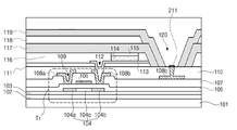
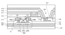
도 2a와 도 2b는 본 발명의 유기발광 다이오드 표시패널의 단면을 나타낸 도면이다.
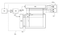
도 3은 본 발명의 유기발광 다이오드 표시장치의 전체 구성을 나타낸 도면이다.
102 : 멀티 버퍼층 103 : 액티브 버퍼층
104 : 반도체층(104a : 소스 영역, 104b : 드레인 영역, 104c : 액티브 영역)
105 : 게이트 절연층 106 : 게이트 전극
107 : 층간 절연층 108a : 소스 전극
108b : 드레인 전극 109 : 소스 및 드레인 컨택홀
110 : 보호층 111 : 평탄화층
112 : 드레인 컨택홀 113 : 제 1 전극
114 : 유기발광층 115 : 제 2 전극
116 : 뱅크 117 : 제 1 봉지층
118 : 유기막층 119 : 제 2 봉지층
120 : 봉지층 컨택홀 211 : 터치전극
300 : 터치패널 구동부 310 : 터치입력 제어부
320 : Tx 구동부 330 : Rx 구동부
400 : 타이밍 제어부 500 : 게이트 구동부
600 : 데이터 구동부 700 : 호스트 시스템
Claims (8)
- 제 1 기판과;
상기 제 1 기판 상에 형성되는 박막 트랜지스터와;
상기 박막 트랜지스터를 덮는 보호층과;
상기 보호층 상에 형성되는 봉지층을 포함하고,
상기 봉지층에는 상기 보호층의 일부를 노출시키는 봉지층 컨택홀이 형성되고, 상기 보호층이 노출된 영역의 상부에는 터치전극이 형성되며, 상기 터치전극은 상기 박막 트랜지스터의 드레인 전극 또는 상기 제 1 기판 상에 형성되는 제 1 라인과 연결되는 유기발광 다이오드 표시장치.
- 제 1 항에 있어서,
상기 제 1 기판은 폴리이미드로 형성되는 유기발광 다이오드 표시장치.
- 제 1 항에 있어서,
상기 봉지층은 무기막층인 제 1 봉지층 및 제 2 봉지층과 유기막층을 포함하고,
상기 제 1 봉지층과 상기 제 2 봉지층 사이에는 유기막층이 형성되어 박막 봉지층을 이루는 유기발광 다이오드 표시장치.
- 제 1 항에 있어서,
상기 제 1 기판 상에 멀티 버퍼층과 액티브 버퍼층이 순차적으로 형성되고,
상기 액티브 버퍼층 상에 상기 박막 트랜지스터가 형성되며,
상기 박막 트랜지스터 상에 상기 보호층과 평탄화층이 순차적으로 형성되고,
상기 평탄화층 상에는 유기발광 다이오드와 이를 둘러싸는 뱅크가 형성되며,
상기 유기발광 다이오드와 상기 뱅크 상에는 상기 봉지층이 형성되고,
상기 봉지층 컨택홀은 상기 봉지층 및 상기 뱅크, 상기 평탄화층을 제거하여 상기 보호층의 일부를 노출시키는 유기발광 다이오드 표시장치.
- 제 1 항에 있어서,
상기 보호층은 상기 박막 트랜지스터의 소스 전극 및 드레인 전극 상에 섬 형태로 형성되는 유기발광 다이오드 표시장치.
- 제 1 항 내지 제 5 항 중 어느 하나의 항에 있어서,
베젤영역이 아닌 비표시영역에 위치하는 터치패널 구동부를 포함하며,
상기 터치패널 구동부는 상기 제 1 라인을 통하여 터치입력 구동신호를 상기 터치전극으로 전송하고,
상기 터치전극은 상기 제 1 라인을 통하여 터치입력 감지신호를 상기 터치패널 구동부로 전송하는 유기발광 다이오드 표시장치.
- 제 6 항에 있어서,
상기 제 1 라인은 데이터 라인인 유기발광 다이오드 표시장치.
- 제 6 항에 있어서,
상기 제 1 라인을 통해 상기 터치전극에 구동전원을 인가하는 유기발광 다이오드 표시장치.
Priority Applications (10)
| Application Number | Priority Date | Filing Date | Title |
|---|---|---|---|
| KR1020180172125A KR102695220B1 (ko) | 2018-12-28 | 2018-12-28 | 터치 타입 유기발광 다이오드 표시장치 |
| US16/578,695 US11296156B2 (en) | 2018-11-28 | 2019-09-23 | Organic light emitting diode device |
| CN202311785145.2A CN117915696A (zh) | 2018-11-28 | 2019-11-21 | 有机发光二极管器件 |
| EP19210556.7A EP3660913A3 (en) | 2018-11-28 | 2019-11-21 | Organic light emitting diode device |
| CN201911147652.7A CN111244132B (zh) | 2018-11-28 | 2019-11-21 | 有机发光二极管器件 |
| TW108143188A TWI776099B (zh) | 2018-11-28 | 2019-11-27 | 有機發光二極體裝置 |
| TW113122687A TW202442100A (zh) | 2018-11-28 | 2019-11-27 | 有機發光二極體裝置 |
| TW111128187A TWI849463B (zh) | 2018-11-28 | 2019-11-27 | 有機發光二極體裝置 |
| JP2019215337A JP6887009B2 (ja) | 2018-11-28 | 2019-11-28 | 有機発光ダイオード装置 |
| US17/679,061 US12426468B2 (en) | 2018-11-28 | 2022-02-23 | Organic light emitting diode device |
Applications Claiming Priority (1)
| Application Number | Priority Date | Filing Date | Title |
|---|---|---|---|
| KR1020180172125A KR102695220B1 (ko) | 2018-12-28 | 2018-12-28 | 터치 타입 유기발광 다이오드 표시장치 |
Publications (2)
| Publication Number | Publication Date |
|---|---|
| KR20200082012A true KR20200082012A (ko) | 2020-07-08 |
| KR102695220B1 KR102695220B1 (ko) | 2024-08-13 |
Family
ID=71601184
Family Applications (1)
| Application Number | Title | Priority Date | Filing Date |
|---|---|---|---|
| KR1020180172125A Active KR102695220B1 (ko) | 2018-11-28 | 2018-12-28 | 터치 타입 유기발광 다이오드 표시장치 |
Country Status (1)
| Country | Link |
|---|---|
| KR (1) | KR102695220B1 (ko) |
Cited By (1)
| Publication number | Priority date | Publication date | Assignee | Title |
|---|---|---|---|---|
| US12317725B2 (en) | 2022-09-28 | 2025-05-27 | Samsung Display Co., Ltd. | Display device having an input sensing layer including a dummy electrode and method of manufacturing the same |
Citations (2)
| Publication number | Priority date | Publication date | Assignee | Title |
|---|---|---|---|---|
| WO2016163367A1 (ja) * | 2015-04-09 | 2016-10-13 | シャープ株式会社 | El表示装置およびel表示装置の製造方法 |
| KR20180043528A (ko) * | 2016-10-20 | 2018-04-30 | 주식회사 실리콘웍스 | 인셀 터치 유기발광표시장치 및 그 구동회로 |
-
2018
- 2018-12-28 KR KR1020180172125A patent/KR102695220B1/ko active Active
Patent Citations (2)
| Publication number | Priority date | Publication date | Assignee | Title |
|---|---|---|---|---|
| WO2016163367A1 (ja) * | 2015-04-09 | 2016-10-13 | シャープ株式会社 | El表示装置およびel表示装置の製造方法 |
| KR20180043528A (ko) * | 2016-10-20 | 2018-04-30 | 주식회사 실리콘웍스 | 인셀 터치 유기발광표시장치 및 그 구동회로 |
Cited By (1)
| Publication number | Priority date | Publication date | Assignee | Title |
|---|---|---|---|---|
| US12317725B2 (en) | 2022-09-28 | 2025-05-27 | Samsung Display Co., Ltd. | Display device having an input sensing layer including a dummy electrode and method of manufacturing the same |
Also Published As
| Publication number | Publication date |
|---|---|
| KR102695220B1 (ko) | 2024-08-13 |
Similar Documents
| Publication | Publication Date | Title |
|---|---|---|
| JP6887009B2 (ja) | 有機発光ダイオード装置 | |
| US11675466B2 (en) | Touch sensor, touch sensor driving method, and display device | |
| US20160132148A1 (en) | Organic light-emitting diode (oled) display | |
| US20180088726A1 (en) | Organic Light-Emitting Display Panel and Organic Light-Emitting Display Device Having Built-In Touchscreen | |
| EP4160366B1 (en) | Display device | |
| KR20180059633A (ko) | 플렉서블 전계발광 표시장치 | |
| US12248646B2 (en) | Detection device | |
| TW202309871A (zh) | 顯示裝置 | |
| KR20210079614A (ko) | 유기발광 표시장치 | |
| KR102695220B1 (ko) | 터치 타입 유기발광 다이오드 표시장치 | |
| KR20230151587A (ko) | 표시 장치 | |
| JP2025128267A (ja) | 表示装置 | |
| US20240224631A1 (en) | Display Device | |
| KR102703482B1 (ko) | 표시 장치 | |
| EP4024175B1 (en) | Display panel and display device | |
| EP4521895B1 (en) | Display apparatus | |
| US20250182520A1 (en) | Display apparatus | |
| US20260090218A1 (en) | Display device |
Legal Events
| Date | Code | Title | Description |
|---|---|---|---|
| PA0109 | Patent application |
Patent event code: PA01091R01D Comment text: Patent Application Patent event date: 20181228 |
|
| PG1501 | Laying open of application | ||
| A201 | Request for examination | ||
| PA0201 | Request for examination |
Patent event code: PA02012R01D Patent event date: 20211112 Comment text: Request for Examination of Application Patent event code: PA02011R01I Patent event date: 20181228 Comment text: Patent Application |
|
| E902 | Notification of reason for refusal | ||
| PE0902 | Notice of grounds for rejection |
Comment text: Notification of reason for refusal Patent event date: 20230905 Patent event code: PE09021S01D |
|
| E701 | Decision to grant or registration of patent right | ||
| PE0701 | Decision of registration |
Patent event code: PE07011S01D Comment text: Decision to Grant Registration Patent event date: 20240516 |
|
| GRNT | Written decision to grant | ||
| PR0701 | Registration of establishment |
Comment text: Registration of Establishment Patent event date: 20240809 Patent event code: PR07011E01D |
|
| PR1002 | Payment of registration fee |
Payment date: 20240809 End annual number: 3 Start annual number: 1 |
|
| PG1601 | Publication of registration |