KR20200083395A - 비휘발성 메모리 장치 및 이의 제조 방법 - Google Patents
비휘발성 메모리 장치 및 이의 제조 방법 Download PDFInfo
- Publication number
- KR20200083395A KR20200083395A KR1020200074210A KR20200074210A KR20200083395A KR 20200083395 A KR20200083395 A KR 20200083395A KR 1020200074210 A KR1020200074210 A KR 1020200074210A KR 20200074210 A KR20200074210 A KR 20200074210A KR 20200083395 A KR20200083395 A KR 20200083395A
- Authority
- KR
- South Korea
- Prior art keywords
- channel
- film
- layer
- upper channel
- memory device
- Prior art date
- Legal status (The legal status is an assumption and is not a legal conclusion. Google has not performed a legal analysis and makes no representation as to the accuracy of the status listed.)
- Granted
Links
Images





Classifications
-
- H—ELECTRICITY
- H10—SEMICONDUCTOR DEVICES; ELECTRIC SOLID-STATE DEVICES NOT OTHERWISE PROVIDED FOR
- H10B—ELECTRONIC MEMORY DEVICES
- H10B43/00—EEPROM devices comprising charge-trapping gate insulators
- H10B43/20—EEPROM devices comprising charge-trapping gate insulators characterised by three-dimensional [3D] arrangements, e.g. with cells on different height levels
- H10B43/23—EEPROM devices comprising charge-trapping gate insulators characterised by three-dimensional [3D] arrangements, e.g. with cells on different height levels with source and drain on different levels, e.g. with sloping channels
- H10B43/27—EEPROM devices comprising charge-trapping gate insulators characterised by three-dimensional [3D] arrangements, e.g. with cells on different height levels with source and drain on different levels, e.g. with sloping channels the channels comprising vertical portions, e.g. U-shaped channels
-
- H01L27/11582—
-
- H01L21/02532—
-
- H01L21/02598—
-
- H01L21/02667—
-
- H01L21/28518—
-
- H01L21/28525—
-
- H01L21/76877—
-
- H01L27/1157—
-
- H—ELECTRICITY
- H10—SEMICONDUCTOR DEVICES; ELECTRIC SOLID-STATE DEVICES NOT OTHERWISE PROVIDED FOR
- H10B—ELECTRONIC MEMORY DEVICES
- H10B43/00—EEPROM devices comprising charge-trapping gate insulators
- H10B43/30—EEPROM devices comprising charge-trapping gate insulators characterised by the memory core region
- H10B43/35—EEPROM devices comprising charge-trapping gate insulators characterised by the memory core region with cell select transistors, e.g. NAND
-
- H—ELECTRICITY
- H10—SEMICONDUCTOR DEVICES; ELECTRIC SOLID-STATE DEVICES NOT OTHERWISE PROVIDED FOR
- H10D—INORGANIC ELECTRIC SEMICONDUCTOR DEVICES
- H10D64/00—Electrodes of devices having potential barriers
- H10D64/01—Manufacture or treatment
- H10D64/011—Manufacture or treatment of electrodes ohmically coupled to a semiconductor
- H10D64/0111—Manufacture or treatment of electrodes ohmically coupled to a semiconductor to Group IV semiconductors
- H10D64/0112—Manufacture or treatment of electrodes ohmically coupled to a semiconductor to Group IV semiconductors using conductive layers comprising silicides
-
- H—ELECTRICITY
- H10—SEMICONDUCTOR DEVICES; ELECTRIC SOLID-STATE DEVICES NOT OTHERWISE PROVIDED FOR
- H10D—INORGANIC ELECTRIC SEMICONDUCTOR DEVICES
- H10D64/00—Electrodes of devices having potential barriers
- H10D64/01—Manufacture or treatment
- H10D64/011—Manufacture or treatment of electrodes ohmically coupled to a semiconductor
- H10D64/0111—Manufacture or treatment of electrodes ohmically coupled to a semiconductor to Group IV semiconductors
- H10D64/0113—Manufacture or treatment of electrodes ohmically coupled to a semiconductor to Group IV semiconductors the conductive layers comprising highly doped semiconductor materials, e.g. polysilicon layers or amorphous silicon layers
-
- H—ELECTRICITY
- H10—SEMICONDUCTOR DEVICES; ELECTRIC SOLID-STATE DEVICES NOT OTHERWISE PROVIDED FOR
- H10P—GENERIC PROCESSES OR APPARATUS FOR THE MANUFACTURE OR TREATMENT OF DEVICES COVERED BY CLASS H10
- H10P14/00—Formation of materials, e.g. in the shape of layers or pillars
- H10P14/20—Formation of materials, e.g. in the shape of layers or pillars of semiconductor materials
- H10P14/34—Deposited materials, e.g. layers
- H10P14/3402—Deposited materials, e.g. layers characterised by the chemical composition
- H10P14/3404—Deposited materials, e.g. layers characterised by the chemical composition being Group IVA materials
- H10P14/3411—Silicon, silicon germanium or germanium
-
- H—ELECTRICITY
- H10—SEMICONDUCTOR DEVICES; ELECTRIC SOLID-STATE DEVICES NOT OTHERWISE PROVIDED FOR
- H10P—GENERIC PROCESSES OR APPARATUS FOR THE MANUFACTURE OR TREATMENT OF DEVICES COVERED BY CLASS H10
- H10P14/00—Formation of materials, e.g. in the shape of layers or pillars
- H10P14/20—Formation of materials, e.g. in the shape of layers or pillars of semiconductor materials
- H10P14/34—Deposited materials, e.g. layers
- H10P14/3451—Structure
- H10P14/3452—Microstructure
- H10P14/3458—Monocrystalline
-
- H—ELECTRICITY
- H10—SEMICONDUCTOR DEVICES; ELECTRIC SOLID-STATE DEVICES NOT OTHERWISE PROVIDED FOR
- H10P—GENERIC PROCESSES OR APPARATUS FOR THE MANUFACTURE OR TREATMENT OF DEVICES COVERED BY CLASS H10
- H10P14/00—Formation of materials, e.g. in the shape of layers or pillars
- H10P14/20—Formation of materials, e.g. in the shape of layers or pillars of semiconductor materials
- H10P14/38—Formation of materials, e.g. in the shape of layers or pillars of semiconductor materials characterised by treatments done after the formation of the materials
- H10P14/3802—Crystallisation or recrystallisation of non-monocrystalline semiconductor materials, e.g. regrowth
-
- H—ELECTRICITY
- H10—SEMICONDUCTOR DEVICES; ELECTRIC SOLID-STATE DEVICES NOT OTHERWISE PROVIDED FOR
- H10W—GENERIC PACKAGES, INTERCONNECTIONS, CONNECTORS OR OTHER CONSTRUCTIONAL DETAILS OF DEVICES COVERED BY CLASS H10
- H10W20/00—Interconnections in chips, wafers or substrates
- H10W20/01—Manufacture or treatment
- H10W20/031—Manufacture or treatment of conductive parts of the interconnections
- H10W20/056—Manufacture or treatment of conductive parts of the interconnections by filling conductive material into holes, grooves or trenches
Landscapes
- Chemical & Material Sciences (AREA)
- Crystallography & Structural Chemistry (AREA)
- Semiconductor Memories (AREA)
- Non-Volatile Memory (AREA)
Abstract
Description
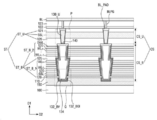
도 2는 몇몇 실시예들에 따른 비휘발성 메모리 장치를 설명하기 위한 단면도이다.
도 3a 내지 3d는 도 2의 P 영역을 설명하기 위한 다양한 도면들이다.
도 4a 및 4b는 도 2의 Q 영역을 설명하기 위한 다양한 도면들이다.
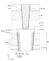
도 5는 몇몇 실시예들에 따른 비휘발성 메모리 장치를 설명하기 위한 단면도이다.
도 6a 내지 6d는 도 5의 P 영역을 설명하기 위한 다양한 도면들이다.
도 7은 몇몇 실시예들에 따른 비휘발성 메모리 장치를 설명하기 위한 단면도이다.
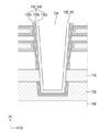
도 8 내지 13은 몇몇 실시예들에 따른 비휘발성 메모리 장치를 설명하기 위한 중간단계 도면들이다.
120: 절연막 CS: 채널 구조체
130_B: 하부 채널막 SSL: 상부 도전 전극
130_U: 상부 채널막 CH_PAD: 채널 패드 패턴
140: 실리사이드막 134: 수직 절연 패턴
Claims (10)
- 기판;
상기 기판 상에, 제1 방향으로 적층된 복수의 하부 도전 전극을 포함하는 하부 적층 구조체;
상기 하부 적층 구조체 상에, 상부 도전 전극을 포함하는 상부 적층 구조체;
상기 하부 적층 구조체를 관통하여, 상기 제1 방향으로 연장되는 하부 채널막을 포함하는 하부 채널 구조체; 및
상기 상부 적층 구조체를 관통하여, 상기 제1 방향으로 연장되는 상부 채널막을 포함하는 상부 채널 구조체를 포함하고,
상기 상부 채널막은 상기 하부 채널막과 접촉하고,
상기 하부 채널막과 상기 상부 채널막 사이의 경계에서, 상기 하부 채널막의 제2 방향으로의 폭은 상기 상부 채널막의 상기 제2 방향으로의 폭보다 크고,
상기 상부 채널막은 단결정 실리콘으로 형성되고,
상기 하부 채널막은 다결정 실리콘을 포함하는 비휘발성 메모리 장치. - 제 1항에 있어서,
상기 상부 도전 전극은 다결정 실리콘 도전막을 포함하고,
상기 하부 도전 전극은 금속성 도전막을 포함하는 비휘발성 메모리 장치. - 제 1항에 있어서,
상기 복수의 하부 도전 전극은 상기 상부 도전 전극에 최인접하는 제1 하부 도전 전극을 포함하고,
상기 하부 채널막과 상기 상부 채널막 사이의 경계는 상기 제1 하부 도전 전극의 상면과 상기 상부 도전 전극의 하면 사이에 위치하는 비휘발성 메모리 장치. - 제 1항에 있어서,
상기 하부 채널막은 채널 패드 패턴을 포함하고,
상기 채널 패드 패턴은 다결정 실리콘을 포함하는 비휘발성 메모리 장치. - 제 4항에 있어서,
상기 채널 패드 패턴의 상면을 따라 연장된 실리사이드막을 더 포함하는 비휘발성 메모리 장치. - 제 1항에 있어서,
상기 하부 채널막은 채널 패드 패턴을 포함하고,
상기 채널 패드 패턴은 단결정 실리콘을 포함하는 비휘발성 메모리 장치. - 제 6항에 있어서,
상기 채널 패드 패턴의 하면을 따라 연장된 실리사이드막을 더 포함하는 비휘발성 메모리 장치. - 제 1항에 있어서,
상기 상부 채널 구조체는 상부 수직 절연 패턴을 더 포함하고,
상기 상부 채널막은 상기 상부 수직 절연 패턴의 측벽을 따라 연장되는 비휘발성 메모리 장치. - 제 1항에 있어서,
상기 상부 채널막 상에 배치되고, 도핑된 불순물을 포함하는 비트 라인 패드를 더 포함하는 비휘발성 메모리 장치. - 기판 상에, 몰드 절연막 및 희생 절연막이 교대로 적층된 하부 몰드 구조체를 형성하고,
상기 하부 몰드 구조체를 관통하고, 하부 채널막을 포함하는 하부 채널 구조체를 형성하고,
상기 하부 몰드 구조체 상에, 상부 도전막을 포함하는 상부 몰드 구조체를 형성하고,
상기 상부 몰드 구조체를 관통하고, 상기 하부 채널막을 노출시키는 상부 채널 홀을 형성하고,
상기 상부 채널 홀 내에, 상기 하부 채널막과 접촉하는 프리 상부 채널막을 형성하고, 상기 프로 상부 채널막은 비정질 실리콘으로 형성되고,
단결정화 공정을 통해 상기 프리 상부 채널막을 변화시켜, 상기 상부 채널 홀 내에 상부 채널막을 형성하는 것을 포함하고,
상기 단결정화 공정은 MILC(metal induced lateral crystallization) 공정, 레이저 열 어닐링(laser thermal annealing) 공정 및 SEG(selective epitaxial growth) 공정 중 하나를 이용하는 비휘발성 메모리 장치의 제조 방법.
Priority Applications (1)
| Application Number | Priority Date | Filing Date | Title |
|---|---|---|---|
| KR1020200074210A KR102796609B1 (ko) | 2020-06-18 | 2020-06-18 | 비휘발성 메모리 장치 및 이의 제조 방법 |
Applications Claiming Priority (1)
| Application Number | Priority Date | Filing Date | Title |
|---|---|---|---|
| KR1020200074210A KR102796609B1 (ko) | 2020-06-18 | 2020-06-18 | 비휘발성 메모리 장치 및 이의 제조 방법 |
Publications (2)
| Publication Number | Publication Date |
|---|---|
| KR20200083395A true KR20200083395A (ko) | 2020-07-08 |
| KR102796609B1 KR102796609B1 (ko) | 2025-04-15 |
Family
ID=71601430
Family Applications (1)
| Application Number | Title | Priority Date | Filing Date |
|---|---|---|---|
| KR1020200074210A Active KR102796609B1 (ko) | 2020-06-18 | 2020-06-18 | 비휘발성 메모리 장치 및 이의 제조 방법 |
Country Status (1)
| Country | Link |
|---|---|
| KR (1) | KR102796609B1 (ko) |
Cited By (1)
| Publication number | Priority date | Publication date | Assignee | Title |
|---|---|---|---|---|
| US12557280B2 (en) | 2021-09-08 | 2026-02-17 | Samsung Electronics Co., Ltd. | Three-dimensional semiconductor memory device with increased electron mobility and electronic system including the same |
Citations (4)
| Publication number | Priority date | Publication date | Assignee | Title |
|---|---|---|---|---|
| US9397111B1 (en) * | 2015-10-30 | 2016-07-19 | Sandisk Technologies Llc | Select gate transistor with single crystal silicon for three-dimensional memory |
| US9449983B2 (en) * | 2013-12-19 | 2016-09-20 | Sandisk Technologies Llc | Three dimensional NAND device with channel located on three sides of lower select gate and method of making thereof |
| US9922987B1 (en) * | 2017-03-24 | 2018-03-20 | Sandisk Technologies Llc | Three-dimensional memory device containing separately formed drain select transistors and method of making thereof |
| KR20200033067A (ko) * | 2018-09-19 | 2020-03-27 | 에스케이하이닉스 주식회사 | 반도체 장치 및 그 제조방법 |
-
2020
- 2020-06-18 KR KR1020200074210A patent/KR102796609B1/ko active Active
Patent Citations (4)
| Publication number | Priority date | Publication date | Assignee | Title |
|---|---|---|---|---|
| US9449983B2 (en) * | 2013-12-19 | 2016-09-20 | Sandisk Technologies Llc | Three dimensional NAND device with channel located on three sides of lower select gate and method of making thereof |
| US9397111B1 (en) * | 2015-10-30 | 2016-07-19 | Sandisk Technologies Llc | Select gate transistor with single crystal silicon for three-dimensional memory |
| US9922987B1 (en) * | 2017-03-24 | 2018-03-20 | Sandisk Technologies Llc | Three-dimensional memory device containing separately formed drain select transistors and method of making thereof |
| KR20200033067A (ko) * | 2018-09-19 | 2020-03-27 | 에스케이하이닉스 주식회사 | 반도체 장치 및 그 제조방법 |
Cited By (1)
| Publication number | Priority date | Publication date | Assignee | Title |
|---|---|---|---|---|
| US12557280B2 (en) | 2021-09-08 | 2026-02-17 | Samsung Electronics Co., Ltd. | Three-dimensional semiconductor memory device with increased electron mobility and electronic system including the same |
Also Published As
| Publication number | Publication date |
|---|---|
| KR102796609B1 (ko) | 2025-04-15 |
Similar Documents
| Publication | Publication Date | Title |
|---|---|---|
| US12225725B2 (en) | Semiconductor devices and manufacturing methods of the same | |
| US12327757B2 (en) | Three-dimensional semiconductor device | |
| US11864382B2 (en) | Three-dimensional semiconductor memory device with vertical channels in a connection region having a lower channel pattern contacting the substrate | |
| US10615124B2 (en) | Three-dimensional semiconductor device including a cell array region and a contact region | |
| US11211402B2 (en) | Three-dimensional semiconductor memory device | |
| US11910611B2 (en) | Nonvolatile memory device and method for fabricating the same | |
| US12200936B2 (en) | 3D semiconductor memory device and method of fabricating same | |
| JP7743227B2 (ja) | 半導体メモリ装置 | |
| CN106558591A (zh) | 三维半导体器件 | |
| US12310026B2 (en) | Semiconductor memory device and method of fabricating the same | |
| KR102850151B1 (ko) | 반도체 메모리 장치 | |
| KR102796609B1 (ko) | 비휘발성 메모리 장치 및 이의 제조 방법 | |
| KR102801018B1 (ko) | 반도체 메모리 장치 및 이의 제조 방법 | |
| CN116419568A (zh) | 存储器件及其制造方法及包括存储器件的电子设备 | |
| KR102926832B1 (ko) | 반도체 메모리 장치 및 이의 제조 방법 |
Legal Events
| Date | Code | Title | Description |
|---|---|---|---|
| PA0109 | Patent application |
St.27 status event code: A-0-1-A10-A12-nap-PA0109 |
|
| PG1501 | Laying open of application |
St.27 status event code: A-1-1-Q10-Q12-nap-PG1501 |
|
| P22-X000 | Classification modified |
St.27 status event code: A-2-2-P10-P22-nap-X000 |
|
| P22-X000 | Classification modified |
St.27 status event code: A-2-2-P10-P22-nap-X000 |
|
| A201 | Request for examination | ||
| PA0201 | Request for examination |
St.27 status event code: A-1-2-D10-D11-exm-PA0201 |
|
| E902 | Notification of reason for refusal | ||
| PE0902 | Notice of grounds for rejection |
St.27 status event code: A-1-2-D10-D21-exm-PE0902 |
|
| P11-X000 | Amendment of application requested |
St.27 status event code: A-2-2-P10-P11-nap-X000 |
|
| P13-X000 | Application amended |
St.27 status event code: A-2-2-P10-P13-nap-X000 |
|
| E701 | Decision to grant or registration of patent right | ||
| PE0701 | Decision of registration |
St.27 status event code: A-1-2-D10-D22-exm-PE0701 |
|
| GRNT | Written decision to grant | ||
| PR0701 | Registration of establishment |
St.27 status event code: A-2-4-F10-F11-exm-PR0701 |
|
| PR1002 | Payment of registration fee |
St.27 status event code: A-2-2-U10-U11-oth-PR1002 Fee payment year number: 1 |
|
| PG1601 | Publication of registration |
St.27 status event code: A-4-4-Q10-Q13-nap-PG1601 |
|
| P22-X000 | Classification modified |
St.27 status event code: A-4-4-P10-P22-nap-X000 |