KR20200083395A - Nonvolatile memory device and method for fabricating the same - Google Patents
Nonvolatile memory device and method for fabricating the same Download PDFInfo
- Publication number
- KR20200083395A KR20200083395A KR1020200074210A KR20200074210A KR20200083395A KR 20200083395 A KR20200083395 A KR 20200083395A KR 1020200074210 A KR1020200074210 A KR 1020200074210A KR 20200074210 A KR20200074210 A KR 20200074210A KR 20200083395 A KR20200083395 A KR 20200083395A
- Authority
- KR
- South Korea
- Prior art keywords
- channel
- film
- layer
- upper channel
- memory device
- Prior art date
- Legal status (The legal status is an assumption and is not a legal conclusion. Google has not performed a legal analysis and makes no representation as to the accuracy of the status listed.)
- Granted
Links
Images





Classifications
-
- H—ELECTRICITY
- H10—SEMICONDUCTOR DEVICES; ELECTRIC SOLID-STATE DEVICES NOT OTHERWISE PROVIDED FOR
- H10B—ELECTRONIC MEMORY DEVICES
- H10B43/00—EEPROM devices comprising charge-trapping gate insulators
- H10B43/20—EEPROM devices comprising charge-trapping gate insulators characterised by three-dimensional [3D] arrangements, e.g. with cells on different height levels
- H10B43/23—EEPROM devices comprising charge-trapping gate insulators characterised by three-dimensional [3D] arrangements, e.g. with cells on different height levels with source and drain on different levels, e.g. with sloping channels
- H10B43/27—EEPROM devices comprising charge-trapping gate insulators characterised by three-dimensional [3D] arrangements, e.g. with cells on different height levels with source and drain on different levels, e.g. with sloping channels the channels comprising vertical portions, e.g. U-shaped channels
-
- H01L27/11582—
-
- H01L21/02532—
-
- H01L21/02598—
-
- H01L21/02667—
-
- H01L21/28518—
-
- H01L21/28525—
-
- H01L21/76877—
-
- H01L27/1157—
-
- H—ELECTRICITY
- H10—SEMICONDUCTOR DEVICES; ELECTRIC SOLID-STATE DEVICES NOT OTHERWISE PROVIDED FOR
- H10B—ELECTRONIC MEMORY DEVICES
- H10B43/00—EEPROM devices comprising charge-trapping gate insulators
- H10B43/30—EEPROM devices comprising charge-trapping gate insulators characterised by the memory core region
- H10B43/35—EEPROM devices comprising charge-trapping gate insulators characterised by the memory core region with cell select transistors, e.g. NAND
-
- H—ELECTRICITY
- H10—SEMICONDUCTOR DEVICES; ELECTRIC SOLID-STATE DEVICES NOT OTHERWISE PROVIDED FOR
- H10D—INORGANIC ELECTRIC SEMICONDUCTOR DEVICES
- H10D64/00—Electrodes of devices having potential barriers
- H10D64/01—Manufacture or treatment
- H10D64/011—Manufacture or treatment of electrodes ohmically coupled to a semiconductor
- H10D64/0111—Manufacture or treatment of electrodes ohmically coupled to a semiconductor to Group IV semiconductors
- H10D64/0112—Manufacture or treatment of electrodes ohmically coupled to a semiconductor to Group IV semiconductors using conductive layers comprising silicides
-
- H—ELECTRICITY
- H10—SEMICONDUCTOR DEVICES; ELECTRIC SOLID-STATE DEVICES NOT OTHERWISE PROVIDED FOR
- H10D—INORGANIC ELECTRIC SEMICONDUCTOR DEVICES
- H10D64/00—Electrodes of devices having potential barriers
- H10D64/01—Manufacture or treatment
- H10D64/011—Manufacture or treatment of electrodes ohmically coupled to a semiconductor
- H10D64/0111—Manufacture or treatment of electrodes ohmically coupled to a semiconductor to Group IV semiconductors
- H10D64/0113—Manufacture or treatment of electrodes ohmically coupled to a semiconductor to Group IV semiconductors the conductive layers comprising highly doped semiconductor materials, e.g. polysilicon layers or amorphous silicon layers
-
- H—ELECTRICITY
- H10—SEMICONDUCTOR DEVICES; ELECTRIC SOLID-STATE DEVICES NOT OTHERWISE PROVIDED FOR
- H10P—GENERIC PROCESSES OR APPARATUS FOR THE MANUFACTURE OR TREATMENT OF DEVICES COVERED BY CLASS H10
- H10P14/00—Formation of materials, e.g. in the shape of layers or pillars
- H10P14/20—Formation of materials, e.g. in the shape of layers or pillars of semiconductor materials
- H10P14/34—Deposited materials, e.g. layers
- H10P14/3402—Deposited materials, e.g. layers characterised by the chemical composition
- H10P14/3404—Deposited materials, e.g. layers characterised by the chemical composition being Group IVA materials
- H10P14/3411—Silicon, silicon germanium or germanium
-
- H—ELECTRICITY
- H10—SEMICONDUCTOR DEVICES; ELECTRIC SOLID-STATE DEVICES NOT OTHERWISE PROVIDED FOR
- H10P—GENERIC PROCESSES OR APPARATUS FOR THE MANUFACTURE OR TREATMENT OF DEVICES COVERED BY CLASS H10
- H10P14/00—Formation of materials, e.g. in the shape of layers or pillars
- H10P14/20—Formation of materials, e.g. in the shape of layers or pillars of semiconductor materials
- H10P14/34—Deposited materials, e.g. layers
- H10P14/3451—Structure
- H10P14/3452—Microstructure
- H10P14/3458—Monocrystalline
-
- H—ELECTRICITY
- H10—SEMICONDUCTOR DEVICES; ELECTRIC SOLID-STATE DEVICES NOT OTHERWISE PROVIDED FOR
- H10P—GENERIC PROCESSES OR APPARATUS FOR THE MANUFACTURE OR TREATMENT OF DEVICES COVERED BY CLASS H10
- H10P14/00—Formation of materials, e.g. in the shape of layers or pillars
- H10P14/20—Formation of materials, e.g. in the shape of layers or pillars of semiconductor materials
- H10P14/38—Formation of materials, e.g. in the shape of layers or pillars of semiconductor materials characterised by treatments done after the formation of the materials
- H10P14/3802—Crystallisation or recrystallisation of non-monocrystalline semiconductor materials, e.g. regrowth
-
- H—ELECTRICITY
- H10—SEMICONDUCTOR DEVICES; ELECTRIC SOLID-STATE DEVICES NOT OTHERWISE PROVIDED FOR
- H10W—GENERIC PACKAGES, INTERCONNECTIONS, CONNECTORS OR OTHER CONSTRUCTIONAL DETAILS OF DEVICES COVERED BY CLASS H10
- H10W20/00—Interconnections in chips, wafers or substrates
- H10W20/01—Manufacture or treatment
- H10W20/031—Manufacture or treatment of conductive parts of the interconnections
- H10W20/056—Manufacture or treatment of conductive parts of the interconnections by filling conductive material into holes, grooves or trenches
Landscapes
- Chemical & Material Sciences (AREA)
- Crystallography & Structural Chemistry (AREA)
- Semiconductor Memories (AREA)
- Non-Volatile Memory (AREA)
Abstract
Description
본 발명은 비휘발성 메모리 장치 및 이의 제조 방법에 관한 것으로, 좀 더 구체적으로, 본 발명은 상부 채널막이 단결정 실리콘으로 형성되는 비휘발성 메모리 장치 및 이의 제조 방법에 관한 것이다.The present invention relates to a nonvolatile memory device and a method for manufacturing the same, and more particularly, the present invention relates to a nonvolatile memory device in which the upper channel film is formed of single crystal silicon and a method for manufacturing the same.
반도체 메모리 장치는 크게 휘발성 메모리 장치와 비휘발성 메모리 장치로 구분될 수 있다.The semiconductor memory device can be roughly classified into a volatile memory device and a nonvolatile memory device.
소비자가 요구하는 우수한 성능 및 저렴한 가격을 충족시키기 위해 반도체 장치의 집적도를 증가시키는 것이 요구되고 있다. 반도체 장치의 경우, 그 집적도는 제품의 가격을 결정하는 중요한 요인이기 때문에, 특히 증가된 집적도가 요구되고 있다. 따라서, 최근에는 단위 메모리 셀을 수직으로 배치하는 3차원 메모리 장치가 개발되고 있다.In order to meet the excellent performance and low price required by consumers, it is required to increase the integration density of semiconductor devices. In the case of a semiconductor device, since the integration degree is an important factor in determining the price of a product, an increase in integration degree is particularly required. Therefore, in recent years, three-dimensional memory devices in which unit memory cells are vertically arranged have been developed.
메모리 셀을 수직으로 배치하는 3차원 메모리 장치는 세대가 거듭됨에 따라 채널막에서의 전기적 특성의 열화가 주요 이슈로 부각되고 있으며, 이를 극복하기 위해 다양한 공정이 개발되고 있다. In a three-dimensional memory device in which memory cells are vertically disposed, deterioration of electrical characteristics in a channel film is a major issue as generations continue, and various processes have been developed to overcome this.
본 발명이 해결하려는 과제는, 스트링 선택 라인에 배치되는 채널막의 저항 및 저항 성분 등을 감소시키는 비휘발성 메모리 장치를 제공하는 것이다. An object of the present invention is to provide a nonvolatile memory device that reduces resistance and resistance components of a channel film disposed on a string selection line.
본 발명이 해결하려는 과제는, 스트링 선택 라인에 배치되는 채널막의 저항 및 저항 성분 등을 감소시키는 비휘발성 메모리 장치의 제조 방법을 제공하는 것이다.The problem to be solved by the present invention is to provide a method of manufacturing a nonvolatile memory device that reduces resistance and resistance components of a channel film disposed on a string selection line.
본 발명이 해결하려는 과제들은 이상에서 언급한 과제들로 제한되지 않으며, 언급되지 않은 또 다른 과제들은 아래의 기재로부터 당업자에게 명확하게 이해될 수 있을 것이다. The problems to be solved by the present invention are not limited to the problems mentioned above, and other problems not mentioned will be clearly understood by those skilled in the art from the following description.
상기 기술적 과제를 달성하기 위한 본 발명의 몇몇 실시예에 따른 비휘발성 메모리 장치는, 기판, 기판 상에, 제1 방향으로 적층된 복수의 하부 도전 전극을 포함하는 하부 적층 구조체, 하부 적층 구조체 상에, 상부 도전 전극을 포함하는 상부 적층 구조체, 하부 적층 구조체를 관통하여, 제1 방향으로 연장되는 하부 채널막을 포함하는 하부 채널 구조체 및 상부 적층 구조체를 관통하여, 제1 방향으로 연장되는 상부 채널막을 포함하는 상부 채널 구조체를 포함하고, 상부 채널막은 하부 채널막과 접촉하고, 하부 채널막과 상부 채널막 사이의 경계에서, 하부 채널막의 제2 방향으로의 폭은 상부 채널막의 제2 방향으로의 폭보다 크고, 상부 채널막은 단결정 실리콘으로 형성되고, 하부 채널막은 다결정 실리콘을 포함한다.Non-volatile memory device according to some embodiments of the present invention for achieving the above technical problem, on a substrate, a substrate, a lower stacked structure including a plurality of lower conductive electrodes stacked in a first direction, on a lower stacked structure , An upper stacked structure including an upper conductive electrode, a lower channel structure passing through the lower stacked structure, and including a lower channel film extending in a first direction, and an upper channel film extending through the upper stacked structure and extending in a first direction. The upper channel structure, the upper channel film is in contact with the lower channel film, and at the boundary between the lower channel film and the upper channel film, the width of the lower channel film in the second direction is greater than the width of the upper channel film in the second direction. The large, upper channel film is formed of monocrystalline silicon, and the lower channel film contains polycrystalline silicon.
상기 기술적 과제를 달성하기 위한 본 발명의 몇몇 실시예에 따른 비휘발성 메모리 제조방법은, 기판 상에, 몰드 절연막 및 희생 절연막이 교대로 적층된 하부 몰드 구조체를 형성하고, 하부 몰드 구조체를 관통하고, 하부 채널막을 포함하는 하부 채널 구조체를 형성하고, 하부 몰드 구조체 상에, 상부 도전막을 포함하는 상부 몰드 구조체를 형성하고, 상부 몰드 구조체를 관통하고, 하부 채널막을 노출시키는 상부 채널 홀을 형성하고, 상부 채널 홀 내에, 하부 채널막과 접촉하는 프리 상부 채널막을 형성하고, 프로 상부 채널막은 비정질 실리콘으로 형성되고, 단결정화 공정을 통해 프리 상부 채널막을 변화시켜, 상부 채널 홀 내에 상부 채널막을 형성하는 것을 포함하고, 단결정화 공정은 MILC(metal induced lateral crystallization) 공정, 레이저 열 어닐링(laser thermal annealing) 공정 및 SEG(selective epitaxial growth) 공정 중 하나를 이용하는 비휘발성 메모리 장치의 제조 방법. 포함한다.A method of manufacturing a nonvolatile memory according to some embodiments of the present invention for achieving the above technical problem, forms a lower mold structure in which a mold insulating film and a sacrificial insulating film are alternately stacked on a substrate, penetrates the lower mold structure, A lower channel structure including a lower channel film is formed, an upper mold structure including an upper conductive film is formed on the lower mold structure, an upper channel hole is formed through the upper mold structure, and an upper channel hole is exposed, and an upper channel hole is formed. In the channel hole, forming a free upper channel film in contact with the lower channel film, the pro upper channel film is formed of amorphous silicon, and changing the free upper channel film through a single crystallization process to form an upper channel film in the upper channel hole The single crystallization process is a method of manufacturing a nonvolatile memory device using one of a metal induced lateral crystallization (MILC) process, a laser thermal annealing process, and a selective epitaxial growth (SEG) process. Includes.
기타 실시예들의 구체적인 사항들은 상세한 설명 및 도면들에 포함되어 있다.Specific details of other embodiments are included in the detailed description and drawings.
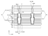
도 1은 몇몇 실시예들에 따른 비휘발성 메모리 장치를 설명하기 위한 예시적인 회로도이다.
도 2는 몇몇 실시예들에 따른 비휘발성 메모리 장치를 설명하기 위한 단면도이다.
도 3a 내지 3d는 도 2의 P 영역을 설명하기 위한 다양한 도면들이다.
도 4a 및 4b는 도 2의 Q 영역을 설명하기 위한 다양한 도면들이다.
도 5는 몇몇 실시예들에 따른 비휘발성 메모리 장치를 설명하기 위한 단면도이다.
도 6a 내지 6d는 도 5의 P 영역을 설명하기 위한 다양한 도면들이다.
도 7은 몇몇 실시예들에 따른 비휘발성 메모리 장치를 설명하기 위한 단면도이다.
도 8 내지 13은 몇몇 실시예들에 따른 비휘발성 메모리 장치를 설명하기 위한 중간단계 도면들이다.1 is an exemplary circuit diagram for describing a nonvolatile memory device in accordance with some embodiments.
2 is a cross-sectional view illustrating a nonvolatile memory device in accordance with some embodiments.
3A to 3D are various views for describing the region P in FIG. 2.
4A and 4B are various views for describing the Q region of FIG. 2.
5 is a cross-sectional view illustrating a nonvolatile memory device in accordance with some embodiments.
6A to 6D are various views for describing the P region of FIG. 5.
7 is a cross-sectional view illustrating a nonvolatile memory device in accordance with some embodiments.
8 to 13 are intermediate stage diagrams for describing a nonvolatile memory device according to some embodiments.
도 1은 몇몇 실시예들에 따른 비휘발성 메모리 장치를 설명하기 위한 예시적인 회로도이다.1 is an exemplary circuit diagram for describing a nonvolatile memory device in accordance with some embodiments.
도 1을 참고하면, 몇몇 실시예들에 따른 비휘발성 메모리 장치의 메모리 셀 어레이는 공통 소오스 라인(CSL), 복수의 비트 라인들(BL0-BL2) 및 공통 소오스 라인(CSL)과 비트 라인들(BL0-BL2) 사이에 배치되는 복수의 셀 스트링들(CSTR)을 포함할 수 있다.Referring to FIG. 1, a memory cell array of a nonvolatile memory device according to some embodiments includes a common source line (CSL), a plurality of bit lines (BL0-BL2), and a common source line (CSL) and bit lines ( BL0-BL2) may include a plurality of cell strings CSTR.
비트 라인들(BL0-BL2) 각각에 복수의 셀 스트링들(CSTR)이 병렬로 연결될 수 있다. 복수의 셀 스트링들(CSTR)은 공통 소오스 라인(CSL)에 공통으로 연결될 수 있다. 즉, 복수의 비트 라인들(BL0-BL2)과 하나의 공통 소오스 라인(CSL) 사이에 복수의 셀 스트링들(CSTR)이 배치될 수 있다. 공통 소오스 라인(CSL)은 복수로 2차원적으로 배열될 수 있다. 여기서, 공통 소오스 라인들(CSL)에는 전기적으로 동일한 전압이 인가될 수 있거나, 또는 공통 소오스 라인들(CSL) 각각이 전기적으로 제어될 수도 있다.A plurality of cell strings CSTR may be connected to each of the bit lines BL0-BL2 in parallel. The plurality of cell strings CSTR may be commonly connected to the common source line CSL. That is, a plurality of cell strings CSTR may be disposed between the plurality of bit lines BL0-BL2 and one common source line CSL. The common source lines CSL may be arranged in two dimensions in plural. Here, the same voltage may be applied to the common source lines CSL, or each of the common source lines CSL may be electrically controlled.
예를 들어, 각각의 셀 스트링들(CSTR)은 스트링 선택 트랜지스터(SST), 직렬 연결된 메모리 셀들(MCT), 접지 선택 트랜지스터(GST)로 구성될 수 있다. 또한, 메모리 셀들(MCT) 각각은 데이터 저장 요소(data storage element)를 포함한다.For example, each cell string CSTR may include a string select transistor SST, series-connected memory cells MCT, and a ground select transistor GST. In addition, each of the memory cells MCT includes a data storage element.
일 예로, 각각의 셀 스트링들(CSTR)은 비트 라인(BL0-BL2)과 직렬로 연결된 스트링 선택 트랜지스터(SST)을 포함할 수 있다. 접지 선택 트랜지스터(GST)는 공통 소오스 라인(CSL)에 접속될 수 있다. 메모리 셀들(MCT)은 스트링 선택 트랜지스터(SST)와 접지 선택 트랜지스터(GST) 사이에 직렬 연결될 수 있다.For example, each cell string CSTR may include a string select transistor SST connected in series with the bit lines BL0-BL2. The ground select transistor GST may be connected to the common source line CSL. The memory cells MCT may be connected in series between the string select transistor SST and the ground select transistor GST.
나아가, 각각의 셀 스트링들(CSTR)은 스트링 선택 트랜지스터(SST)와 메모리 셀(MCT) 사이에 연결된 더미 셀(DMCT)을 더 포함할 수 있다. Furthermore, each cell string CSTR may further include a dummy cell DMCT connected between the string select transistor SST and the memory cell MCT.
도면에는 도시하지 않았으나, 더미 셀(DMCT)은 접지 선택 트랜지스터(GST)와 메모리 셀(MCT) 사이에도 연결될 수 있다. 다른 예로, 각각의 셀 스트링들(CSTR)에서 접지 선택 트랜지스터(GST)는 직렬 연결된 복수 개의 모스(MOS) 트랜지스터들로 구성될 수도 있다. 또 다른 예로, 각각의 셀 스트링들(CSTR)은 직렬 연결된 복수의 스트링 선택 트랜지스터를 포함할 수도 있다. 또 다른 예로, 각각의 셀 스트링들(CSTR)는 비트 라인(BL0-BL2)과 스트링 선택 트랜지스터(SST) 사이에 배치되는 소거 제어 트랜지스터를 더 포함할 수 있다. 소거 제어 트랜지스터는 스트링 선택 트랜지스터(SST)와 직렬로 연결될 수 있다. Although not shown in the drawing, the dummy cell DMCT may be connected between the ground selection transistor GST and the memory cell MCT. As another example, the ground select transistor GST in each cell string CSTR may be composed of a plurality of MOS transistors connected in series. As another example, each cell string CSTR may include a plurality of string select transistors connected in series. As another example, each cell string CSTR may further include an erase control transistor disposed between the bit lines BL0-BL2 and the string select transistor SST. The erase control transistor may be connected in series with the string selection transistor SST.
몇몇 실시예들에 따르면, 스트링 선택 트랜지스터(SST)는 스트링 선택 라인(SSL)에 의해 제어될 수 있다. 메모리 셀들(MCT)은 복수 개의 워드 라인들(WL0-WLn)에 의해 제어될 수 있으며, 더미 셀들(DMCT)은 더미 워드 라인(DWL)에 의해 제어될 수 있다. 또한, 접지 선택 트랜지스터(GST)는 접지 선택 라인(GSL)에 의해 제어될 수 있다. 공통 소오스 라인(CSL)은 접지 선택 트랜지스터들(GST)의 소오스들에 공통으로 연결될 수 있다.According to some embodiments, the string select transistor SST may be controlled by the string select line SSL. The memory cells MCT may be controlled by a plurality of word lines WL0-WLn, and the dummy cells DMCT may be controlled by a dummy word line DWL. Also, the ground select transistor GST may be controlled by the ground select line GSL. The common source line CSL may be commonly connected to the sources of the ground selection transistors GST.
하나의 셀 스트링(CSTR)은 공통 소오스 라인들(CSL)로부터의 거리가 서로 다른 복수개의 메모리 셀들(MCT)로 구성될 수 있다. 그리고, 공통 소오스 라인들(CSL)과 비트 라인들(BL0-BL2) 사이에는 복수 개의 워드 라인들(WL0-WLn, DWL)이 배치될 수 있다. One cell string CSTR may be formed of a plurality of memory cells MCT having different distances from the common source lines CSL. In addition, a plurality of word lines WL0-WLn and DWL may be disposed between the common source lines CSL and the bit lines BL0-BL2.
공통 소오스 라인들(CSL)로부터 실질적으로 동일한 거리에 배치되는, 메모리 셀들(MCT)의 게이트 전극들은 워드 라인들(WL0-WLn, DWL) 중의 하나에 공통으로 연결되어 등전위 상태에 있을 수 있다. 이와 달리, 메모리 셀들(MCT)의 게이트 전극들이 공통 소오스 라인들(CSL)로부터 실질적으로 동일한 레벨에 배치되더라도, 서로 다른 행 또는 열에 배치되는 게이트 전극들이 독립적으로 제어될 수 있다.The gate electrodes of the memory cells MCT, which are disposed at substantially the same distance from the common source lines CSL, may be in an equipotential state by being commonly connected to one of the word lines WL0-WLn and DWL. Alternatively, even if the gate electrodes of the memory cells MCT are disposed at substantially the same level from the common source lines CSL, the gate electrodes disposed in different rows or columns can be independently controlled.
접지 선택 라인들(GSL0-GSL2) 및 스트링 선택 라인들(SSL)은 예를 들어, 워드 라인들(WL0-WLn, DWL)과 같은 방향으로 연장될 수 있다. 공통 소오스 라인들(CSL)로부터 실질적으로 동일한 레벨에 배치되는 접지 선택 라인들(GSL0-GSL2) 및 스트링 선택 라인(SSL)은 전기적으로 서로 분리될 수 있다.The ground select lines GSL0-GSL2 and the string select lines SSL may extend in the same direction as, for example, the word lines WL0-WLn and DWL. The ground select lines GSL0-GSL2 and the string select line SSL that are disposed at substantially the same level from the common source lines CSL may be electrically separated from each other.
도면에 도시되지 않았지만, 셀 스트링(CSTR)이 소거 제어 트랜지스터를 포함할 경우, 소거 제어 트랜지스터들은 공통의 소거 제어 라인에 의해 제어될 수 있다. 소거 제어 트랜지스터들은 메모리 셀 어레이의 소거 동작시 게이트 유도 드레인 누설(GIDL; Gate Induced Drain Leakage)을 발생시킨다. 즉, 소거 제어 트랜지스터들은 GIDL 트랜지스터일 수 있다.Although not shown in the figure, when the cell string CSTR includes an erase control transistor, the erase control transistors can be controlled by a common erase control line. The erase control transistors generate a gate induced drain leakage (GIDL) during an erase operation of the memory cell array. That is, the erase control transistors may be GIDL transistors.
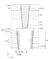
도 2는 몇몇 실시예들에 따른 비휘발성 메모리 장치를 설명하기 위한 단면도이다. 도 3a 내지 3d는 도 2의 P 영역을 설명하기 위한 다양한 도면들이다. 도 4a 및 4b는 도 2의 Q 영역을 설명하기 위한 다양한 도면들이다. 2 is a cross-sectional view illustrating a nonvolatile memory device in accordance with some embodiments. 3A to 3D are various views for describing the region P in FIG. 2. 4A and 4B are various views for describing the Q region of FIG. 2.
도 2 내지 4b를 참고하면, 몇몇 실시예들에 따른 비휘발성 메모리 장치는 기판(100), 하부 적층 구조체(ST_B), 상부 적층 구조체(ST_U), 하부 채널 구조체(CS_B), 단결정 실리콘으로 형성된 상부 채널막(130_U)를 포함하는 상부 채널 구조체(CS_U) 및 복수의 비트 라인(BL)들을 포함할 수 있다.2 to 4B, a nonvolatile memory device according to some embodiments includes a
기판(100)은 실리콘 기판, 실리콘게르마늄 기판, 게르마늄 기판, SGOI(silicon germanium on insulator), SOI(silicon-on-insulator), GOI(Germanium-On-Insulator) 중 하나를 포함할 수 있다. 또는, 기판(100)은 안티몬화 인듐, 납 텔루르 화합물, 인듐 비소, 인듐 인화물, 갈륨 비소 또는 안티몬화 갈륨 등과 같은 반도체 물질을 포함할 수 있으나, 이에 한정되는 것은 아니다.The
수평 도전 기판(150)은 기판(100) 상에 배치될 수 있다. 수평 도전 기판(150)은 공통 소오스 플레이트일 수 있다. 즉, 수평 도전 기판(150)은 도 1의 공통 소오스 라인(CSL)의 역할을 할 수 있다.The horizontal
수평 도전 기판(150)는 도전성의 반도체막, 금속 실리사이드막 및 금속막 중 적어도 하나를 포함할 수 있다. 수평 도전 기판(150)가 도전성의 반도체막을 포함할 경우, 수평 도전 기판(150)는 예를 들어, 실리콘(Si), 게르마늄(Ge), 실리콘 게르마늄(SiGe), 갈륨비소(GaAs), 인듐갈륨비소(InGaAs), 알루미늄갈륨비소(AlGaAs), 또는 이들의 조합 중 적어도 하나를 포함할 수 있다. 수평 도전 기판(150)은 단결정, 비정질 및 다결정 중에서 선택된 적어도 하나를 포함하는 결정 구조를 가질 수 있다. 수평 도전 기판(150)는 반도체막에 포함된 p형 불순물, n형 불순물 및 탄소 중 적어도 하나를 포함할 수 있다.The horizontal
적층 구조체(ST)는 수평 도전 기판(150) 상에 배치될 수 있다. 적층 구조체(ST)는 하부 적층 구조체(ST_B)와 상부 적층 구조체(ST_U)를 포함할 수 있다. The stacked structure ST may be disposed on the horizontal
하부 적층 구조체(ST_B)는 제1 방향(D1)으로 적층된 복수의 하부 도전 전극들(GSL, WL0 - WLn, DWL)과 복수의 전극간 절연막(120, 125)을 포함할 수 있다. 전극간 절연막(120, 125)은 제1 방향(D1) 방향으로 이격된 하부 도전 전극들(GSL, WL0 - WLn, DWL) 사이에 배치된다.The lower stack structure ST_B may include a plurality of lower conductive electrodes GSL, WL 0 -WL n and DWL stacked in the first direction D1 and a plurality of inter-electrode insulating
복수의 하부 도전 전극들(GSL, WL0 - WLn, DWL)은 접지 선택 라인(GSL), 복수의 워드 라인들(WL0 - WLn), 더미 워드 라인(DWL)을 포함할 수 있다. 접지 선택 라인(GSL), 복수의 워드 라인들(WL0 - WLn), 더미 워드 라인(DWL)은 기판(100) 상에 순차적으로 적층될 수 있다.The plurality of lower conductive electrodes GSL, WL 0 -WL n , and DWL may include a ground selection line GSL, a plurality of word lines WL 0 -WL n , and a dummy word line DWL. The ground selection line GSL, the plurality of word lines WL 0 to WL n , and the dummy word line DWL may be sequentially stacked on the
상부 적층 구조체(ST_U)는 하부 적층 구조체(ST_B) 상에, 제1 방향(D1)으로 적층된 상부 도전 전극(SSL)과 구조체간 절연막(126)을 포함할 수 있다. 구조체간 절연막(126)은 상부 도전 전극(SSL)과 하부 적층 구조체(ST_B)의 최상부에 배치된 하부 도전 전극, 예를 들어 더미 워드 라인(DWL) 사이에 배치된다.The upper stacked structure ST_U may include the upper conductive electrode SSL and the interlayer insulating
도 2에서, 접지 선택 라인(GSL) 상에 5개의 워드 라인(WL0 - WLn)만을 도시하였지만, 이는 설명의 편의를 위한 것일 뿐, 이에 제한되는 것은 아니다. 또한, 하부 적층 구조체(ST_B)의 최상부에 배치된 하부 도전 전극은 더미 워드 라인(DWL)인 것으로 도시하였지만, 이에 제한되는 것은 아니다. 도 1의 셀 스트링(CSTR)이 더미 셀(DMCT)을 포함하지 않을 경우, 적층 구조체(ST)의 최상부에 배치된 하부 도전 전극은 워드 라인(WLn)일 수 있음은 물론이다. In FIG. 2, only five word lines WL 0 to WLn are illustrated on the ground selection line GSL, but this is for convenience of description and is not limited thereto. In addition, the lower conductive electrode disposed on the top of the lower stacked structure ST_B is illustrated as a dummy word line DWL, but is not limited thereto. When the cell string CSTR of FIG. 1 does not include the dummy cell DMCT, the lower conductive electrode disposed on the top of the stack structure ST may be a word line WL n .
하부 적층 구조체(ST_B)는 제1 하부 서브 적층 구조체(ST_B_1)와, 제1 하부 서브 적층 구조체(ST_B_1) 상의 제2 하부 서브 적층 구조체(ST_B_2)를 포함할 수 있다. 제1 하부 서브 적층 구조체(ST_B_1)는 접지 선택 라인(GSL)과 일부의 워드 라인들(WL0 - WLk)을 포함할 수 있다. 제2 하부 서브 적층 구조체(ST_B_2)는 나머지 워드 라인들(WLk+1 - WLn)과 더미 워드 라인(DWL)을 포함할 수 있다. 여기에서, n은 k보다 큰 자연수이다. The lower stacked structure ST_B may include a first lower sub stacked structure ST_B_1 and a second lower sub stacked structure ST_B_2 on the first lower sub stacked structure ST_B_1. The first lower sub-stack structure ST_B_1 may include a ground selection line GSL and some word lines WL 0 -WL k . The second lower sub-stack structure ST_B_2 may include the remaining word lines WL k+1 -WL n and a dummy word line DWL. Here, n is a natural number greater than k.
제1 하부 서브 적층 구조체(ST_B_1)의 최상부에 위치하는 워드 라인(WLk)과, 제2 하부 서브 적층 구조체(ST_B_2)의 최하부에 위치하는 워드 라인(WLk+1) 사이의 전극간 절연막(125)은 제1 하부 서브 적층 구조체(ST_B_1) 및 제2 하부 서브 적층 구조체(ST_B_2) 내의 전극간 절연막(120)의 두께보다 두껍다. The inter-electrode insulating layer between the word line WL k positioned at the top of the first lower sub-layered structure ST_B_1 and the word line WL k+1 positioned at the bottom of the second lower sub-layered structure ST_B_2 ( 125) is thicker than the thickness of the inter-electrode
상부 도전 전극(SSL)은 상부 적층 구조체(ST_U) 상에 배치될 수 있다. 일 예로, 상부 도전 전극(SSL)은 도 1의 스트링 선택 라인의 역할을 할 수 있다. 상부 도전 전극(SSL)은 도 1의 스트링 선택 트랜지스터(SST)에 포함될 수 있다. 다른 예로, 상부 도전 전극(SSL)의 일부는 도 1의 스트링 선택 라인의 역할을 할 수 있다. 상부 도전 전극(SSL)의 나머지는 도 1에 도시되지 않았지만, 소거 제어 트랜지스터에 포함된 소거 제어 라인을 할 수도 있다. 상부 도전 전극(SSL)은 하부 도전 전극들(GSL, WL0 - WLn, DWL)의 두께보다 두껍다.The upper conductive electrode SSL may be disposed on the upper stacked structure ST_U. For example, the upper conductive electrode SSL may serve as the string selection line of FIG. 1. The upper conductive electrode SSL may be included in the string select transistor SST of FIG. 1. As another example, a portion of the upper conductive electrode SSL may serve as the string selection line of FIG. 1. The rest of the upper conductive electrode SSL is not shown in FIG. 1, but an erase control line included in the erase control transistor may be used. The upper conductive electrode SSL is thicker than the thickness of the lower conductive electrodes GSL, WL 0 -WL n , DWL.
상부 도전 전극(SSL)은 하부 적층 구조체(ST_B)와 반대되는 상면과, 하부 적층 구조체(ST_B)와 마주보는 하면을 포함할 수 있다. 상부 도전 전극의 하면은 더미 워드 라인(DWL)을 바라본다. 상부 도전 전극의 하면과, 더미 워드 라인(DWL)의 상면 사이에, 구조체간 절연막(126)이 배치될 수 있다. 구조체간 절연막(126)은 제1 하부 서브 적층 구조체(ST_B_1) 및 제2 하부 서브 적층 구조체(ST_B_2) 내의 전극간 절연막(120)의 두께보다 두껍다.The upper conductive electrode SSL may include an upper surface opposite to the lower stacked structure ST_B, and a lower surface facing the lower stacked structure ST_B. The lower surface of the upper conductive electrode looks at the dummy word line DWL. An inter-structure
하부 도전 전극(GSL, WL0 - WLn, DWL)은 상부 도전 전극(SSL)과 다른 물질을 포함한다. 예를 들어, 하부 도전 전극(GSL, WL0 - WLn, DWL)은 금속성 물질을 포함할 수 있고, 상부 도전 전극(SSL)은 반도체 물질을 포함할 수 있다. 하부 도전 전극(GSL, WL0 - WLn, DWL)은 상부 도전 전극(SSL)과 서로 다른 제조 공정에서 형성될 수 있다. The lower conductive electrode (GSL, WL 0 -WL n , DWL) includes a different material from the upper conductive electrode (SSL). For example, the lower conductive electrode (GSL, WL 0 -WL n , DWL) may include a metallic material, and the upper conductive electrode (SSL) may include a semiconductor material. The lower conductive electrodes GSL, WL 0 -WL n , and DWL may be formed in different manufacturing processes from the upper conductive electrode SSL.
하부 도전 전극들(GSL, WL0 - WLn, DWL)은 예를 들어, 텅스텐(W), 코발트(Co), 니켈(Ni) 등의 금속을 포함할 수 있지만, 금속의 종류는 이에 제한되지 않는다. 도 3a 내지 도 4b에서, 하부 도전 전극(GSL, WL0 - WLn, DWL)은 다중막으로 형성되는 것으로 도시되었지만, 설명의 편의를 위한 것일 뿐, 이에 제한되는 것은 아니다. The lower conductive electrodes (GSL, WL 0 -WL n , DWL) may include, for example, metal such as tungsten (W), cobalt (Co), nickel (Ni), but the type of metal is not limited thereto. Does not. 3A to 4B, the lower conductive electrodes GSL, WL 0 -WL n , and DWL are illustrated as being formed of a multi-layer film, but are for convenience of description and are not limited thereto.
하부 도전 전극(GSL, WL0 - WLn, DWL)은 배리어 도전막(BML)과 필링 도전막(FML)을 포함할 수 있다. 필링 도전막(FML)은 수직 하부 채널막(130_BV) 상에 배치된다. 배리어 도전막(BML)은 필링 도전막(FML) 및 수직 하부 채널막(130_BV) 사이에 배치된다. The lower conductive electrodes GSL, WL 0 -WL n , and DWL may include a barrier conductive layer BML and a peeling conductive layer FML. The peeling conductive film FML is disposed on the vertical lower channel film 130_BV. The barrier conductive layer BML is disposed between the filling conductive layer FML and the vertical lower channel layer 130_BV.
배리어 도전막(BML)은 금속, 금속 질화물, 금속 탄질화물 및 2차원 물질(Two-dimensional(2D) material) 중 적어도 하나를 포함할 수 있다. 예를 들어, 2차원 물질은 금속성 물질 및/또는 반도체성 물질일 수 있다. 2차원 물질(2D material)은 2차원 동소체(allotrope) 또는 2차원 화합물(compound)를 포함할 수 있다. 필링 도전막(FML)은 텅스텐(W), 코발트(Co), 니켈(Ni) 등의 금속을 포함할 수 있지만, 금속의 종류는 이에 제한되지 않는다.The barrier conductive layer (BML) may include at least one of metal, metal nitride, metal carbonitride, and two-dimensional (2D) material. For example, the two-dimensional material can be a metallic material and/or a semiconducting material. The 2D material may include a 2D allotrope or a 2D compound. The peeling conductive film FML may include metals such as tungsten (W), cobalt (Co), and nickel (Ni), but the type of the metal is not limited thereto.
상부 도전 전극(SSL)은 예를 들어, 실리콘(Si), 게르마늄(Ge) 및 실리콘 게르마늄(SiGe) 중 적어도 하나를 포함할 수 있다. 또는, 상부 도전 전극(SSL)은 III-V 화합물 반도체 중 적어도 하나를 포함할 수 있다. 상부 도전 전극은 단결정, 비정질 및 다결정 중에서 선택된 적어도 하나를 포함하는 결정 구조를 가질 수 있다. 상부 도전 전극(SSL)은 반도체막에 포함된 p형 불순물, n형 불순물 및 탄소 중 적어도 하나를 더 포함할 수 있다.The upper conductive electrode SSL may include, for example, at least one of silicon (Si), germanium (Ge), and silicon germanium (SiGe). Alternatively, the upper conductive electrode (SSL) may include at least one of III-V compound semiconductors. The upper conductive electrode may have a crystal structure including at least one selected from single crystal, amorphous and polycrystalline. The upper conductive electrode SSL may further include at least one of p-type impurities, n-type impurities, and carbon included in the semiconductor film.
전극간 절연막(120, 125)과, 구조체간 절연막(126)은 예를 들어, 실리콘 산화물을 포함할 수 있지만, 이에 제한되는 것은 아니다. The inter-electrode
채널 구조체(CS)는 제1 방향(D1)으로 연장된다. 채널 구조체(CS)는 하부 적층 구조체(ST_B) 및 상부 적층 구조체(ST_U)를 관통할 수 있다. 채널 구조체(CS)는 상부 적층 구조체(ST_U) 내에 배치되는 상부 채널 구조체(CS_U)와, 하부 적층 구조체(ST_B) 내에 배치되는 하부 채널 구조체(CS_B)를 포함할 수 있다. The channel structure CS extends in the first direction D1. The channel structure CS may penetrate the lower stacked structure ST_B and the upper stacked structure ST_U. The channel structure CS may include an upper channel structure CS_U disposed in the upper stack structure ST_U and a lower channel structure CS_B disposed in the lower stack structure ST_B.
상부 채널 구조체(CS_U)의 크기는 하부 채널 구조체(CS_B)의 크기보다 작다. 즉, 상부 채널 구조체(CS_U)의 제2 방향(D2)으로의 폭은 하부 채널 구조체(CS_B)의 제2 방향(D2)으로의 폭보다 작다. 즉, 상부 채널막(130_U)과 하부 채널막(130_B) 사이의 경계에서, 하부 채널막(130_B)의 제2 방향(D2)으로의 폭은 상부 채널막의 제2 방향(D2)으로의 폭보다 크다. The size of the upper channel structure CS_U is smaller than the size of the lower channel structure CS_B. That is, the width of the upper channel structure CS_U in the second direction D2 is smaller than the width of the lower channel structure CS_B in the second direction D2. That is, at the boundary between the upper channel layer 130_U and the lower channel layer 130_B, the width of the lower channel layer 130_B in the second direction D2 is greater than the width of the
상부 채널 구조체(CS_U)는 비트 라인(BL)에서 하부 채널 구조체(CS_B)를 향해 제1 방향(D1)으로 멀어짐에 따라 제2 방향(D2)으로의 폭은 감소할 수 있다. As the upper channel structure CS_U moves away from the bit line BL in the first direction D1 toward the lower channel structure CS_B, the width in the second direction D2 may decrease.
비트 라인 패드(BL_PAD)는 상부 채널 구조체(CS_U) 상에 배치된다. 비트 라인 패드(BL_PAD)는 도전성 물질을 포함할 수 있다. 예를 들어, 비트 라인 패드(BL_PAD)는 n형 불순물이 도핑된 반도체 물질을 포함할 수 있다. The bit line pad BL_PAD is disposed on the upper channel structure CS_U. The bit line pad BL_PAD may include a conductive material. For example, the bit line pad BL_PAD may include a semiconductor material doped with n-type impurities.
하부 채널 구조체(CS_B)는 하부 채널막(130_B)과, 수직 절연 패턴(134)을 포함할 수 있다. 하부 채널막(130_B)은 채널 패드 패턴(CH_PAD)과 수직 하부 채널막(130_BV)을 포함할 수 있다. 수직 하부 채널막(130_BV)은 하부 채널 구조체(CS_B)의 측벽을 따라 제1 방향(D1)으로 연장될 수 있다. 수직 절연 패턴(134)은 채널 패드 패턴(CH_PAD)과 수직 하부 채널막(130_BV)에 의해 정의된 공간일 수 있다. 하부 채널막(130_B)은 하부 적층 구조체(ST_B)를 관통한다. 수직 하부 채널막(130_BV)은 공통 소스 라인의 역할을 하는 수평 도전 기판(150)과 전기적으로 연결될 수 있다. The lower channel structure CS_B may include a lower channel layer 130_B and a vertical
채널 패드 패턴(CH_PAD)은 상부 채널막(130_U)과 수직 하부 채널막(130_BV) 사이에 위치할 수 있다. 채널 패드 패턴(CH_PAD)은 수직 하부 채널막(130_BV)과 상부 채널막(130_U)을 전기적으로 연결한다. The channel pad pattern CH_PAD may be positioned between the upper channel layer 130_U and the vertical lower channel layer 130_BV. The channel pad pattern CH_PAD electrically connects the vertical lower channel layer 130_BV and the upper channel layer 130_U.
수직 하부 채널막(130_BV)은 제1 방향(D1)으로 연장되는 측벽부와, 수직 하부 채널막(130_BV)의 측벽부를 연결하는 바닥부를 포함할 수 있다. 수직 하부 채널막(130_BV)의 측벽부는 내부에 할로우 공간(hollow space)를 갖는 파이프 형상, 예를 들어, 원통 형상 또는 마카로니 형상을 가질 수 있다. The vertical lower channel layer 130_BV may include a side wall portion extending in the first direction D1 and a bottom portion connecting the side wall portion of the vertical lower channel layer 130_BV. The sidewall portion of the vertical lower channel layer 130_BV may have a pipe shape having a hollow space therein, for example, a cylindrical shape or a macaroni shape.
하부 채널막(130_B)은 하부 적층 구조체(ST_B) 내에 배치될 수 있다. 수직 하부 채널막(130_BV)은 적층 구조체(ST)에 포함된 워드 라인들(WL0 - WLn), 접지 선택 라인(GSL) 및 더미 워드 라인(DWL)의 측벽을 따라 연장될 수 있다. The lower channel layer 130_B may be disposed in the lower stacked structure ST_B. The vertical lower channel layer 130_BV may extend along sidewalls of the word lines WL 0 to WL n , the ground selection line GSL, and the dummy word line DWL included in the stack structure ST.
상부 채널막(130_U)은 상부 적층 구조체(ST_U)를 관통하고, 비트 라인 패드(BL_PAD)와 접촉할 수 있다. 상부 채널막(130_U)과, 수직 하부 채널막(130_BV)은 각각 제1 방향(D1)으로 연장될 수 있다. 구조에 따라 제1 방향(D1)에 대해 기울기를 갖으면서 연장될 수 있다. 채널 패드 패턴(CH_PAD)은 제2 방향(D2)로 연장될 수 있다.The upper channel layer 130_U may penetrate the upper stacked structure ST_U and contact the bit line pad BL_PAD. The upper channel layer 130_U and the vertical lower channel layer 130_BV may extend in the first direction D1, respectively. Depending on the structure, it may extend while having a slope with respect to the first direction D1. The channel pad pattern CH_PAD may extend in the second direction D2.
수직 하부 채널막(130_BV)은 예를 들어, 실리콘(Si), 게르마늄(Ge) 또는 이들의 혼합물과 같은 반도체 물질을 포함할 수 있다. 또는, 수직 하부 채널막(130_BV)은 금속 산화물 반도체 물질, 유기 반도체 물질 및 탄소 나노 구조체 등의 반도체 물질을 포함할 수도 있다. 상부 채널막(130_U)은 단결정 실리콘으로 형성될 수 있다. The vertical lower channel layer 130_BV may include, for example, a semiconductor material such as silicon (Si), germanium (Ge), or a mixture thereof. Alternatively, the vertical lower channel layer 130_BV may include a semiconductor material such as a metal oxide semiconductor material, an organic semiconductor material, and a carbon nano structure. The upper channel layer 130_U may be formed of single crystal silicon.
도 3a 내지 3d에서 하부 채널막(130_B)은 수직 하부 채널막(130_BV)의 상부에 위치하는 채널 패드 패턴(CH_PAD)을 포함할 수 있다. 채널 패드 패턴(CH_PAD)은 수직 하부 채널막(130_BV)과 상부 채널막(130_U) 사이에 위치할 수 있다. 3A to 3D, the lower channel layer 130_B may include a channel pad pattern CH_PAD positioned above the vertical lower channel layer 130_BV. The channel pad pattern CH_PAD may be positioned between the vertical lower channel layer 130_BV and the upper channel layer 130_U.
몇몇 실시예들에 따른 비휘발성 메모리 장치에서, 채널 패드 패턴(CH_PAD)은 다결정 실리콘을 포함할 수 있다. 반면, 상부 채널막(130_U)은 단결정 실리콘을 포함할 수 있다.In a nonvolatile memory device according to some embodiments, the channel pad pattern CH_PAD may include polycrystalline silicon. On the other hand, the upper channel layer 130_U may include single crystal silicon.
채널 패드 패턴(CH_PAD)은 상부 채널막(130_U)과, 수직 하부 채널막(130_BV)을 전기적으로 연결한다. 채널 패드 패턴(CH_PAD)의 하면은 수직 하부 채널막(130_BV)과 연결되고, 채널 패드 패턴(CH_PAD)의 상면은 상부 채널막(130_U)의 하면과 연결된다. The channel pad pattern CH_PAD electrically connects the upper channel layer 130_U and the vertical lower channel layer 130_BV. The lower surface of the channel pad pattern CH_PAD is connected to the vertical lower channel layer 130_BV, and the upper surface of the channel pad pattern CH_PAD is connected to the lower surface of the upper channel layer 130_U.
채널 패드 패턴(CH_PAD)은 예를 들어, 실리콘(Si), 게르마늄(Ge) 또는 이들의 혼합물과 같은 반도체 물질을 포함할 수 있다. 몇몇 실시예들에 따른 비휘발성 메모리 장치에서, 하부 채널막(130_BV)은 다결정 실리콘을 포함할 수 있다.The channel pad pattern CH_PAD may include, for example, a semiconductor material such as silicon (Si), germanium (Ge), or a mixture thereof. In a nonvolatile memory device according to some embodiments, the lower channel layer 130_BV may include polycrystalline silicon.
도 3a 및 도 3b를 참고하면, 상부 채널막(130_U)은 속이 채워진 기둥 형상일 수 있다. 3A and 3B, the upper channel layer 130_U may have a pillar shape filled in.
도 3c 및 도 3d를 참고하면, 상부 채널 구조체(CS_U)는 수직 절연 패턴(134)을 포함할 수 있다. 수직 절연 패턴(134)은 예를 들어, 실리콘 산화물, 실리콘 산질화물 및 저유전율 물질 중 적어도 하나를 포함할 수 있지만, 이에 제한되는 것은 아니다. 상부 채널막(130_U)은 제1 방향(D1)으로 연장되는 측벽부와, 상부 채널막(130_U)의 측벽부를 연결하는 바닥부를 포함할 수 있다. 상부 채널막(130_U)의 측벽부는 내부에 할로우 공간(hollow space)를 갖는 파이프 형상, 예를 들어, 원통 형상 또는 마카로니 형상을 가질 수 있다.3C and 3D, the upper channel structure CS_U may include a
몇몇 실시예에 따른 비휘발성 메모리 장치는, 채널 패드 패턴(CH_PAD)의 상면을 따라 연장된 실리사이드막(140)을 더 포함할 수 있다. 실리사이드막(140)은 상부 채널막(130_U)과 채널 패드 패턴(CH_PAD)의 경계에 위치할 수 있다. 상부 채널막(130_U)과 채널 패드 패턴(CH_PAD)의 경계는 상부 도전 전극(SSL)에 최인접하는 하부 도전 전극, 예를 들어 더미 워드 라인(DWL)의 상면과 상부 도전 전극(SSL)의 하면 사이에 위치할 수 있다. 실리사이드막(140)은 실리사이드 물질을 포함하고, 예를 들어, 니켈 실리사이드(NiSi), 팔라듐 실리사이드(PdSi), 백금 실리사이드(PtSi) 중 적어도 하나를 포함할 수 있지만, 이에 제한되는 것은 아니다. The nonvolatile memory device according to some embodiments may further include a
도 3a 및 3c를 참고하면, 상부 채널막(130_U)과 채널 패드 패턴(CH_PAD)의 경계에서 실리사이드막(140)이 형성될 수 있다.3A and 3C, a
도 3b 및 도 3d를 참고하면, 실리사이드막(140)이 형성되지 않을 수 있다.Referring to FIGS. 3B and 3D, the
상부 채널 구조체(CS_U)는 상부 채널막(130_U) 및 상부 도전 전극(SSL)에 배치되는 상부 채널 절연막(132_UGI)을 포함할 수 있다. 하부 채널 구조체(CS_B)는 수직 하부 채널막(130_BV) 및 복수의 하부 도전 전극들(GSL, WL0 - WLn, DWL) 사이와, 하부 채널막(130_BV) 및 전극간 절연막(120) 사이에 배치되는 하부 채널 절연막(132_BGI)를 포함할 수 있다. 상부 채널 절연막(132_UGI) 및 하부 채널 절연막(132_BGI)은 상부 채널막(130_U) 및 수직 하부 채널막(130_BV)을 따라 연장될 수 있다. The upper channel structure CS_U may include an upper channel layer 130_U and an upper channel insulating layer 132_UGI disposed on the upper conductive electrode SSL. The lower channel structure CS_B is between the vertical lower channel layer 130_BV and the plurality of lower conductive electrodes GSL, WL 0 -WL n , DWL, and between the lower channel layer 130_BV and the inter-electrode
도 2 내지 4b에서, 하부 채널 절연막(132_BGI)은 예를 들어, 수직 하부 채널막(130_BV) 상에 순차적으로 배치된 터널 절연막(132a), 전하 저장막(132b) 및 블로킹 절연막(132c)을 포함할 수 있다. 터널 절연막(132a), 전하 저장막(132b) 및 블로킹 절연막(132c)은 예시적인 것일 뿐, 이에 제한되는 것은 아니다. 2 to 4B, the lower channel insulating film 132_BGI includes, for example, a
터널 절연막(132a)은 예를 들어, 실리콘 산화물 또는 고유전율 물질(예를 들어, 알루미늄 산화물(Al2O3), 하프늄 산화물(HfO2))을 포함할 수 있다. 전하 저장막(132b)은 예를 들어, 실리콘 질화물을 포함할 수 있다. 블로킹 절연막(132c)은 예를 들어, 실리콘 산화물 또는 고유전율 물질(예를 들어, 알루미늄 산화물(Al2O3), 하프늄 산화물(HfO2))을 포함할 수 있다. 몇몇 실시예들에 따른 비휘발성 메모리 장치에서, 터널 절연막(132a) 및 블로킹 절연막(132c)은 실리콘 산화물을 포함할 수 있다. The
하부 도전 전극들(GSL, WL0 - WLn, DWL)과, 하부 채널 절연막(132_BGI) 사이에, 수평 절연 패턴(HP)이 배치될 수 있다. 수평 절연 패턴(HP)은 예를 들어, 실리콘 산화물 또는 고유전율 물질(예를 들어, 알루미늄 산화물(Al2O3), 하프늄 산화물(HfO2))을 포함할 수 있다. 도시된 것과 달리, 수평 절연 패턴(HP)은 하부 도전 전극들(GSL, WL0 - WLn, DWL)과, 하부 채널 절연막(132_BGI) 사이에 배치되지 않을 수도 있다. A horizontal insulating pattern HP may be disposed between the lower conductive electrodes GSL, WL 0 -WL n , and DWL and the lower channel insulating layer 132_BGI. The horizontal insulating pattern HP may include, for example, silicon oxide or a high-k material (eg, aluminum oxide (Al 2 O 3 ), hafnium oxide (HfO 2 )). Unlike illustrated, the horizontal insulating pattern HP may not be disposed between the lower conductive electrodes GSL, WL 0 -WL n , and DWL, and the lower channel insulating layer 132_BGI.
도 4a에서, 터널 절연막(132a), 전하 저장막(132b) 및 블로킹 절연막(132c)은 수직 하부 채널막(130_BV)의 하부에서 분리될 수 있다. 분리된 터널 절연막(132a), 전하 저장막(132b) 및 블로킹 절연막(132c)은 수직 하부 채널막(130_BV)의 일부를 노출시킬 수 있다. 분리된 터널 절연막(132a), 전하 저장막(132b) 및 블로킹 절연막(132c) 사이로, 수직 구조 지지막(110)이 배치될 수 있다. 수직 구조 지지막(110)은 수평 도전 기판(150)과 수직 하부 채널막(130_BV)을 전기적으로 연결시킬 수 있다. 수직 구조 지지막(110)은 예를 들어, 실리콘(Si), 게르마늄(Ge) 또는 이들의 혼합물과 같은 반도체 물질을 포함할 수 있다.In FIG. 4A, the
도 4b에서, 수평 도전 기판(150)와 적층 구조체(ST) 사이에 수직 구조 지지막(110)이 배치되지 않을 수도 있다. 이와 같은 경우, 수직 하부 채널막(130_BV)의 측벽부가 노출되지 않고, 수직 하부 채널막(130_BV)의 바닥부가 노출될 수 있다. 수직 하부 채널막(130_BV)의 바닥부와 수평 도전 기판(150) 사이의 터널 절연막(132a), 전하 저장막(132b) 및 블로킹 절연막(132c)은 제거될 수 있다. 수직 하부 채널막(130_BV)의 바닥부를 통해, 수직 하부 채널막(130_BV)은 수평 도전 기판(150)과 전기적으로 연결될 수 있다.In FIG. 4B, the vertical
도 2 내지 3d에서, 하부 채널 절연막(132_BGI)과 달리, 상부 채널 절연막(132_UGI)은 예를 들어, 실리콘 산화물을 포함할 수 있다. 도면에는 상부 채널 절연막(132_UGI)은 단일막으로 도시하였지만, 이에 제한되는 것은 아니다. 상부 채널 절연막(132_UGI)은 다중막으로 형성될 수 있다. 일 예로, 몇몇 실시예들에 따른 비휘발성 메모리 장치에서, 상부 채널 절연막(132_UGI)의 적층 구조는 하부 채널 절연막(132_BGI)의 구조와 동일할 수 있다. 다른 예로, 몇몇 실시예들에 따른 비휘발성 메모리 장치에서, 상부 채널 절연막(132_UGI)은 실리콘 산화물 및 고유전율 절연막의 적층 구조를 포함할 수도 있다. 2 to 3D, unlike the lower channel insulating film 132_BGI, the upper channel insulating film 132_UGI may include, for example, silicon oxide. In the drawing, the upper channel insulating layer 132_UGI is illustrated as a single layer, but is not limited thereto. The upper channel insulating layer 132_UGI may be formed of multiple layers. For example, in a nonvolatile memory device according to some embodiments, the stacked structure of the upper channel insulating layer 132_UGI may be the same as that of the lower channel insulating layer 132_BGI. As another example, in the nonvolatile memory device according to some embodiments, the upper channel insulating layer 132_UGI may include a stacked structure of silicon oxide and a high dielectric constant insulating layer.
일 예로, 상부 채널 절연막(132_UGI)은 상부 도전 전극(SSL)과 접촉할 수 있다. 즉, 상부 채널 절연막(132_UGI)과 상부 도전 전극(SSL) 사이에, 금속성 도전 물질이 배치되지 않을 수 있다. 다른 예로, 상부 채널 절연막(132_UGI)은 상부 도전 전극(SSL) 사이에, 도전성 물질을 포함하는 도전성 라이너막이 더 배치될 수 있다. For example, the upper channel insulating layer 132_UGI may contact the upper conductive electrode SSL. That is, a metallic conductive material may not be disposed between the upper channel insulating layer 132_UGI and the upper conductive electrode SSL. As another example, the upper channel insulating layer 132_UGI may further include a conductive liner film including a conductive material between the upper conductive electrodes SSL.
또한, 하부 채널 절연막(132_BGI)은 상부 채널 절연막(132_UGI)과 직접 연결되지 않을 수 있다.Also, the lower channel insulating layer 132_BGI may not be directly connected to the upper channel insulating layer 132_UGI.
상부 도전 전극(SSL) 상에, 제1 내지 제3 층간 절연막(121, 122, 123) 이 순차적으로 배치될 수 있다. 제1 층간 절연막(121) 내에, 비트 라인 패드(BL_PAD)가 배치될 수 있다.On the upper conductive electrode SSL, the first to third
비트 라인(BL)은 상부 도전 전극(SSL) 상에 배치될 수 있다. 비트 라인(BL)은 제2 방향(D2)으로 길게 연장될 수 있다. 비트 라인(BL)은 상부 채널막(130_U) 중 적어도 하나와 전기적으로 연결될 수 있다. 비트 라인(BL)은 제3 층간 절연막(123) 상에 형성될 수 있다. 비트 라인(BL)은 비트 라인 플러그(BLPG)를 매개로 비트 라인 패드(BL_PAD)와 전기적으로 연결될 수 있다.The bit line BL may be disposed on the upper conductive electrode SSL. The bit line BL may be elongated in the second direction D2. The bit line BL may be electrically connected to at least one of the upper channel layers 130_U. The bit line BL may be formed on the third
도 5는 몇몇 실시예들에 따른 비휘발성 메모리 장치를 설명하기 위한 단면도이다. 도 6a 내지 6d는 도 5의 P 영역을 설명하기 위한 다양한 도면들이다. 설명의 편의상, 도 2 내지 4b를 이용하여 설명한 것과 다른 점을 중심으로 설명한다. 5 is a cross-sectional view illustrating a nonvolatile memory device in accordance with some embodiments. 6A to 6D are various views for describing the P region of FIG. 5. For convenience of description, description will be made focusing on differences from those described with reference to FIGS. 2 to 4B.
도 5 내지 도 6d를 참고하면, 몇몇 실시예들에 따른 비휘발성 메모리 장치에서, 하부 채널막(130_B)은 단결정 실리콘으로 형성된 채널 패드 패턴(CH_PAD)을 포함할 수 있다. 하부 채널막(130_B)은 단정결 실리콘으로 형성된 채널 패드 패턴(CH_PAD)과 수직 하부 채널막(130_BV)을 포함한다.5 to 6D, in a nonvolatile memory device according to some embodiments, the lower channel layer 130_B may include a channel pad pattern CH_PAD formed of single crystal silicon. The lower channel layer 130_B includes a channel pad pattern CH_PAD formed of single crystal silicon and a vertical lower channel layer 130_BV.
채널 패드 패턴(CH_PAD)은 상부 채널막(130_U)과 동일 레벨에서 형성될 수 있다. 여기서, "동일 레벨"이라 함은 동일한 제조 공정에 의해 형성되는 것을 의미하는 것이다.The channel pad pattern CH_PAD may be formed at the same level as the upper channel layer 130_U. Here, "same level" means that formed by the same manufacturing process.
채널 패드 패턴(CH_PAD)과 상부 채널막(130_U)은 통합 구조(integral structure)일 수 있다. The channel pad pattern CH_PAD and the upper channel layer 130_U may have an integral structure.
도 2 내지 도 3d와는 달리, 하부 채널 절연막(132_BGI)는 채널 패드 패턴(CH_PAD)의 측벽과 수직 하부 채널막(130_BV)의 측벽을 따라 제1 방향(D1)으로 연장될 수 있다. 구조에 따라 제1 방향(D1)에 대해 기울기를 갖으면서 연장될 수 있다. Unlike in FIGS. 2 to 3D, the lower channel insulating layer 132_BGI may extend in a first direction D1 along a side wall of the channel pad pattern CH_PAD and a vertical lower channel film 130_BV. Depending on the structure, it may extend while having a slope with respect to the first direction D1.
도 6a 및 도 6c를 참고하면, 채널 패드 패턴(CH_PAD)의 하면을 따라 연장되는 실리사이드막(140)을 더 포함할 수 있다. 실리사이드막(140)은 채널 패드 패턴(CH_PAD)과 수직 하부 채널막(130_BV)의 경계에 위치할 수 있다. Referring to FIGS. 6A and 6C, a
도 6a 및 도 6b를 참고하면, 상부 채널막(130_U)은 속이 채워진 기둥 형상일 수 있다. 6A and 6B, the upper channel layer 130_U may have a pillar shape filled with a layer.
도 6c 및 도 6d를 참고하면, 상부 채널 구조체(CS_U)는 수직 절연 패턴(134)을 포함할 수 있다. 수직 절연 패턴(134)은 채널 패드 패턴(CH_PAD) 내에 형성될 수 있다. 수직 절연 패턴(134)은 예를 들어, 실리콘 산화물, 실리콘 산질화물 및 저유전율 물질 중 적어도 하나를 포함할 수 있지만, 이에 제한되는 것은 아니다. 상부 채널막(130_U)은 제1 방향(D1)으로 연장되는 측벽부를 포함할 수 있다. 채널 패드 패턴(CH_PAD)은 제1 방향(D1)으로 연장되는 측벽부, 채널 패드 패턴(CH_PAD)의 측벽부를 연결하는 바닥부 및 채널 패드 패턴(CH_PAD)의 측벽부와 상부 채널막(130_U)의 측벽부를 연결하는 연결부를 포함할 수 있다. 상부 채널막(130_U)의 측벽부와 채널 패드 패턴(CH_PAD)의 측벽부는 내부에 통 형상을 가질 수 있다. 6C and 6D, the upper channel structure CS_U may include a
도 6a 및 6c를 참고하면, 실리사이드막(140)은 채널 패드 패턴(CH_PAD)의 하면을 따라 연장될 수 있다. 즉, 실리사이드막(140)은 채널 패드 패턴(CH_PAD)과 수직 하부 채널막(130_BV)의 경계에 위치한다.6A and 6C, the
도 7은 몇몇 실시예들에 따른 비휘발성 메모리 장치를 설명하기 위한 도면이다. 설명의 편의상, 도 2 내지 4b를 이용하여 설명한 것과 다른 점을 중심으로 설명한다.7 is a diagram for describing a nonvolatile memory device according to some embodiments. For convenience of description, description will be made focusing on differences from those described with reference to FIGS. 2 to 4B.
도 7을 참고하면, 몇몇 실시예들에 따른 비휘발성 메모리 장치는 주변 로직 구조체(PS)와, 셀 어레이 구조체(CAS)를 포함할 수 있다. Referring to FIG. 7, a nonvolatile memory device according to some embodiments may include a peripheral logic structure PS and a cell array structure CAS.
주변 로직 구조체(PS)는 주변 회로(PTR)와, 하부 연결 배선체(PW)와 주변 로직 절연막(101)을 포함할 수 있다. The peripheral logic structure PS may include a peripheral circuit PTR, a lower connection wiring body PW, and a peripheral
주변 회로(PTR)은 기판(100) 상에 형성될 수 있다. 주변 회로(PTR)는 셀 어레이 구조체(CAS)를 동작시키는 회로들일 수 있다.The peripheral circuit PTR may be formed on the
주변 로직 절연막(101)은 기판(100) 상에 형성될 수 있다. 주변 로직 절연막(101)은 예를 들어, 실리콘 산화물, 실리콘 질화물, 실리콘 산질화물 및 저유전율 물질 중 적어도 하나를 포함할 수 있다.The peripheral
하부 연결 배선체(PW)는 주변 로직 절연막(101) 내에 형성될 수 있다. 하부 연결 배선체(PW)는 주변 회로(PTR)와 연결될 수 있다.The lower connection wiring body PW may be formed in the peripheral
셀 어레이 구조체(CAS)는 주변 로직 구조체(PS) 상에 배치될 수 있다. 셀 어레이 구조체(CAS)는 하부 적층 구조체(ST_B), 상부 도전 전극(SSL), 복수의 채널 구조체(CS) 및 복수의 비트 라인(BL)들을 포함할 수 있다. The cell array structure CAS may be disposed on the peripheral logic structure PS. The cell array structure CAS may include a lower stack structure ST_B, an upper conductive electrode SSL, a plurality of channel structures CS, and a plurality of bit lines BL.
수평 도전 기판(150)는 주변 로직 구조체(PS)의 상면을 따라 연장될 수 있다. The horizontal
도시된 것과 달리, 주변 로직 구조체(PS)는 비트라인(BL) 상에 배치될 수 있다. 다르게 설명하면, 상부 도전 전극(SSL)과 주변 로직 구조체(PS) 사이에 비트 라인(BL)이 배치될 수 있다. Unlike illustrated, the peripheral logic structure PS may be disposed on the bit line BL. In other words, the bit line BL may be disposed between the upper conductive electrode SSL and the peripheral logic structure PS.
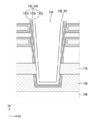
도 8 내지 13은 몇몇 실시예들에 따른 비휘발성 메모리 장치를 설명하기 위한 중간단계 도면들이다. 참고적으로, 도 8 내지 도 13은 도 2의 P 부분에 해당되는 도면일 수 있다. 8 to 13 are intermediate stage diagrams for describing a nonvolatile memory device according to some embodiments. For reference, FIGS. 8 to 13 may be diagrams corresponding to the P portion of FIG. 2.
도 8을 참고하면, 기판(100) 상에, 전극간 절연막(120) 및 희생 절연막(ILD_SC)이 교대로 적층된 몰드 구조체(MS)가 형성될 수 있다.Referring to FIG. 8, a mold structure MS in which an inter-electrode
몰드 구조체(MS) 내에, 몰드 구조체(MS)를 관통하는 하부 채널 구조체(CS_B)가 형성될 수 있다. 하부 채널 구조체(CS_B)는 하부 채널막(130_B), 하부 채널 절연막(132_BGI) 및 수직 절연 패턴(134)을 포함한다. 하부 채널막(130_B)은 수직 하부 채널막(130_BV)과 채널 패드 패턴(CH_PAD)을 포함한다.In the mold structure MS, a lower channel structure CS_B penetrating the mold structure MS may be formed. The lower channel structure CS_B includes a lower channel layer 130_B, a lower channel insulating layer 132_BGI, and a vertical
이어서, 하부 채널 구조체(CS_B) 상에, 구조체간 절연막(126), 상부 도전 전극(SSL) 및 제1 층간 절연막(121)이 순차적으로 적층된다.Subsequently, the inter-structure
상부 도전 전극(SSL) 내에 상부 채널 홀(CH_H)이 형성될 수 있다. 상부 채널 홀(CH_H)은 제1 층간 절연막(121), 상부 도전 전극(SSL) 및 구조체간 절연막(126)을 관통할 수 있다. 상부 채널 홀(CH_H)은 하부 채널 구조체(CS_B) 내의 채널 패드 패턴(CH_PAD)를 노출시킬 수 있다. An upper channel hole CH_H may be formed in the upper conductive electrode SSL. The upper channel hole CH_H may penetrate the first
도 9를 참고하면, 상부 채널 홀(CH_H)의 측벽을 따라 상부 채널 절연막(132_UGI)이 형성될 수 있다. 도면에는 상부 채널 절연막(132_UGI)을 단일막으로 도시하였지만, 이에 제한되는 것은 아니다. 상부 채널 절연막(132_UGI)는 다중막일 수 있고, 하부 채널 절연막(132_UGI)과 동일한 적층 구조일 수 있다.Referring to FIG. 9, an upper channel insulating layer 132_UGI may be formed along sidewalls of the upper channel hole CH_H. Although the upper channel insulating layer 132_UGI is illustrated as a single layer in the drawing, it is not limited thereto. The upper channel insulating film 132_UGI may be a multi-layer film, or may have the same layered structure as the lower channel insulating film 132_UGI.
이어서, 상부 채널 홀(CH_H) 내에, 상부 채널 절연막(132_UGI) 상에, 프리 상부 채널막(130_PR)이 형성될 수 있다. 프리 상부 채널막(130_PR)은 비정질 실리콘으로 형성될 수 있다. 프리 상부 채널막(130_PR)은 상부 채널 홀(CH_H)의 내부를 채울 수 있다. Subsequently, a free upper channel layer 130_PR may be formed on the upper channel insulating layer 132_UGI in the upper channel hole CH_H. The free upper channel layer 130_PR may be formed of amorphous silicon. The free upper channel layer 130_PR may fill the inside of the upper channel hole CH_H.
도 10을 참고하면, 프리 상부 채널막(130_PR)과 제1 층간 절연막(121) 상에 금속막(141)이 형성된다. 금속막(141)은 제2 방향(D2)로 연장된다. 금속막(141)은 예를 들어, 니켈(Ni), 팔라듐(Pd) 및 백금(Pt) 금속을 포함할 수 있지만, 금속의 종류는 이에 제한되지 않는다. Referring to FIG. 10, a
도 11을 참고하면, 실리사이드화 공정을 통해, 금속막(141)의 하부, 즉 금속막(141)과 프리 상부 채널막(130_PR) 사이에 실리사이드막(140)이 형성된다.Referring to FIG. 11, a
도 12를 참고하면, 실리사이드화 공정 후에 남아 있는 금속막(141)이 제거될 수 있다. Referring to FIG. 12, the
도 13을 참고하면, 단결정화 공정을 통해, 프리 상부 채널막(130_PR)은 상부 채널막(130_U)으로 변화될 수 있다. Referring to FIG. 13, through a single crystallization process, the free upper channel film 130_PR may be changed to an upper channel film 130_U.
단결정화 공정을 통해 형성된 상부 채널막(130_U)은 단결정 실리콘으로 형성된다. 단결정화 공정은 MILC(metal induced lateral crystallization) 공정을 이용할 수 있지만, 이에 제한되는 것은 아니다. MILC 공정을 이용하면, 실리사이드막(140)이 프리 상부 채널막(130_PR)의 측벽을 따라 내려가면서 비정질 실리콘이 단결정 실리콘으로 변화된다. 실리사이드막(140)은 하부 채널막(130_BV)과 프리 상부 채널막(130_PR)의 사이에서 멈추게 된다. The upper channel film 130_U formed through the single crystallization process is formed of single crystal silicon. The monocrystallization process may use a metal induced lateral crystallization (MILC) process, but is not limited thereto. When the MILC process is used, the amorphous silicon is changed to single crystal silicon while the
상술한 것과 달리, 단결정화 공정은 레이저 열 어닐링(laser thermal annealing) 공정을 이용할 수 있다. 이 경우에는 실리사이드막(140)이 형성되지 않을 수 있다.Unlike the above, the single crystallization process may use a laser thermal annealing process. In this case, the
도면에는 도시되지 않았지만, 도 3c 및 3d와 같은 비휘발성 메모리 장치를 제공하기 위해, 상부 프리 채널막(130_PR) 상에, 상부 채널 홀(CH_H)의 일부를 채우는 수직 절연 패턴(134)이 형성될 수 있다. 상부 프리 채널막(130_PR)은 제1 방향(D1)으로 연장되는 측벽부와, 상부 프리 채널막(130_PR)의 측벽부를 연결하는 바닥부를 포함할 수 있다. 상부 프리 채널막(130_PR)의 측벽부는 내부에 할로우 공간(hollow space)를 갖는 파이프 형상, 예를 들어, 원통 형상 또는 마카로니 형상을 가질 수 있다.Although not shown in the drawing, in order to provide a nonvolatile memory device as shown in FIGS. 3C and 3D, a vertical
상부 프리 채널막(130_PR)의 측벽부와 바닥부는 위에서 상술한 단결정화 공정을 통해, 비정질 실리콘에서 단결정 실리콘으로 변화할 수 있다.The sidewall portion and the bottom portion of the upper free channel layer 130_PR may be changed from amorphous silicon to single crystal silicon through the single crystallization process described above.
이어서, 도면에는 도시되지 않았지만, 수직 절연 패턴(134) 또는 상부 채널막(130_U) 상에, 상부 채널막(130_U)와 접촉하는 비트 라인 패드(BL_PAD)가 형성될 수 있다.Subsequently, although not illustrated in the drawing, a bit line pad BL_PAD in contact with the upper channel layer 130_U may be formed on the vertical insulating
도 2를 참고하면, 제1 층간 절연막(121) 상에, 비트 라인 패드(BL_PAD)를 덮는 제2 층간 절연막(122)이 형성될 수 있다. 제2 층간 절연막(122) 상에 제3 층간 절연막(123)이 형성될 수 있다.Referring to FIG. 2, a second
제3 층간 절연막(123) 상에 비트 라인(BL)이 형성될 수 있다.A bit line BL may be formed on the third
이어서, 희생 절연막(ILD_SC)를 하부 도전 전극으로 교체할 수 있다.Subsequently, the sacrificial insulating film ILD_SC may be replaced with a lower conductive electrode.
도 6a와 같은 비휘발성 메모리 장치를 제공하기 위해, 도면에 도시되지 않았지만, 상부 채널 홀(CH_H)을 형성하기 전에 채널 패드 패턴(CH_PAD)이 형성되지 않을 수 있다. 즉, 채널 패드 패턴(CH_PAD)을 형성하기 전에 상부 채널 홀(CH_H)이 형성될 수 있다. 이 경우에는 상부 채널 홀(CH_H)이 하부 채널 구조체(CS_B)와 일부분 중첩될 수 있다. 상부 채널 홀(CH_H)은 하부 채널 구조체(CS_B)의 수직 절연 패턴(134)을 노출시킬 수 있다. In order to provide a nonvolatile memory device as shown in FIG. 6A, although not illustrated in the drawing, a channel pad pattern CH_PAD may not be formed before forming the upper channel hole CH_H. That is, the upper channel hole CH_H may be formed before forming the channel pad pattern CH_PAD. In this case, the upper channel hole CH_H may partially overlap the lower channel structure CS_B. The upper channel hole CH_H may expose the vertical insulating
이어서, 상부 채널 구조체(CS_U)와 중첩되는 상부 채널 홀(CH_H)의 측벽을 따라 상부 채널 절연막(132_UGI)이 형성될 수 있다. 하부 채널 구조체(CS_B)와 중첩되는 상부 채널 홀(CH_H)의 측벽에는 상부 채널 절연막(132_UGI)이 형성되지 않을 수 있다.Subsequently, an upper channel insulating layer 132_UGI may be formed along sidewalls of the upper channel hole CH_H overlapping the upper channel structure CS_U. An upper channel insulating layer 132_UGI may not be formed on a sidewall of the upper channel hole CH_H overlapping the lower channel structure CS_B.
이어서, 상부 채널 홀(CH_H) 내에 프리 상부 채널막(130_PR)이 형성될 수 있다. 프리 상부 채널막(130_PR)은 비정질 실리콘으로 형성될 수 있다. Subsequently, a free upper channel layer 130_PR may be formed in the upper channel hole CH_H. The free upper channel layer 130_PR may be formed of amorphous silicon.
이어서, 프리 상부 채널막(130_PR)과 제1 층간 절연막(121) 상에 금속막(141)이 형성된다.Subsequently, a
이어서, 실리사이드화 공정을 통해, 금속막(141)의 하부, 즉 금속막(141)과 프리 상부 채널막(130_PR) 사이에 실리사이드막(140)이 형성된다. Subsequently, a
이어서, 실리사이드화 공정 후에 남아 있는 금속막(141)이 제거될 수 있다.Subsequently, the
이어서, 단결정화 공정을 통해, 프리 상부 채널막(130_PR)은 상부 채널막(130_U)으로 변화될 수 있다. 이 경우에는, 채널 패드 패턴(CH_PAD)이 단결정 실리콘으로 형성될 수 있다. 단결정화 공정은 MILC(metal induced lateral crystallization) 공정을 이용할 수 있지만, 이에 제한되는 것은 아니다. Subsequently, through the single crystallization process, the free upper channel film 130_PR may be changed to the upper channel film 130_U. In this case, the channel pad pattern CH_PAD may be formed of single crystal silicon. The monocrystallization process may use a metal induced lateral crystallization (MILC) process, but is not limited thereto.
MILC 공정을 이용하는 경우, 실리사이드막(140)은 프리 상부 채널막(130_PR)의 측벽을 따라 내려간다. 실리사이드막(140)은 채널 패드 패턴(CH_PAD)과 수직 하부 채널막(130_BV)의 경계에서 멈춘다. 실리사이드막(140)은 채널 패드 패턴(CH_PAD)의 하면을 따라 연장될 수 있다. When using the MILC process, the
프리 상부 채널막(130_PR)을 형성한 후에, 금속막(141)을 형성하지 않고, 레이저 열 어닐링(laser thermal annealing) 공정을 이용하여 상부 채널막(130_U)을 형성할 수 있음은 물론이다.After forming the free upper channel layer 130_PR, the
도면에 도시되지 않았지만, 도 9와 달리, 상부 채널 홀(CH_H) 내부에 프리 상부 채널막(130_PR)이 형성되지 않을 수 있다. 프리 상부 채널막(130_PR)을 형성하지 않고, 상부 채널홀(CH_H) 내부에 상부 채널막(130_U)을 형성할 수 있다. 이 경우에는 SEG(selective epitaxial growth) 공정을 이용할 수 있다. Although not shown in the drawing, unlike in FIG. 9, the free upper channel layer 130_PR may not be formed inside the upper channel hole CH_H. The upper channel layer 130_U may be formed inside the upper channel hole CH_H without forming the free upper channel layer 130_PR. In this case, a selective epitaxial growth (SEG) process can be used.
이상 첨부된 도면을 참조하여 본 발명의 실시예들을 설명하였으나, 본 발명은 상기 실시예들에 한정되는 것이 아니라 서로 다른 다양한 형태로 제조될 수 있으며, 본 발명이 속하는 기술분야에서 통상의 지식을 가진 자는 본 발명의 기술적 사상이나 필수적인 특징을 변경하지 않고서 다른 구체적인 형태로 실시될 수 있다는 것을 이해할 수 있을 것이다. 그러므로 이상에서 기술한 실시예들은 모든 면에서 예시적인 것이며 한정적이 아닌 것으로 이해해야만 한다.The embodiments of the present invention have been described above with reference to the accompanying drawings, but the present invention is not limited to the above embodiments, and may be manufactured in various different forms, and having ordinary knowledge in the technical field to which the present invention pertains. It will be understood that a person can be implemented in other specific forms without changing the technical spirit or essential features of the present invention. Therefore, it should be understood that the embodiments described above are illustrative in all respects and not restrictive.
100: 기판
ST: 적층 구조체
120: 절연막
CS: 채널 구조체
130_B: 하부 채널막
SSL: 상부 도전 전극
130_U: 상부 채널막
CH_PAD: 채널 패드 패턴
140: 실리사이드막
134: 수직 절연 패턴
100: substrate ST: laminated structure
120: insulating film CS: channel structure
130_B: lower channel film SSL: upper conductive electrode
130_U: Upper channel film CH_PAD: Channel pad pattern
140: silicide film 134: vertical insulation pattern
Claims (10)
상기 기판 상에, 제1 방향으로 적층된 복수의 하부 도전 전극을 포함하는 하부 적층 구조체;
상기 하부 적층 구조체 상에, 상부 도전 전극을 포함하는 상부 적층 구조체;
상기 하부 적층 구조체를 관통하여, 상기 제1 방향으로 연장되는 하부 채널막을 포함하는 하부 채널 구조체; 및
상기 상부 적층 구조체를 관통하여, 상기 제1 방향으로 연장되는 상부 채널막을 포함하는 상부 채널 구조체를 포함하고,
상기 상부 채널막은 상기 하부 채널막과 접촉하고,
상기 하부 채널막과 상기 상부 채널막 사이의 경계에서, 상기 하부 채널막의 제2 방향으로의 폭은 상기 상부 채널막의 상기 제2 방향으로의 폭보다 크고,
상기 상부 채널막은 단결정 실리콘으로 형성되고,
상기 하부 채널막은 다결정 실리콘을 포함하는 비휘발성 메모리 장치.Board;
A lower stacked structure including a plurality of lower conductive electrodes stacked on the substrate in a first direction;
An upper stacked structure including an upper conductive electrode on the lower stacked structure;
A lower channel structure including a lower channel film extending through the lower layered structure and extending in the first direction; And
And an upper channel structure including an upper channel film extending in the first direction through the upper stack structure.
The upper channel film is in contact with the lower channel film,
At a boundary between the lower channel film and the upper channel film, a width in the second direction of the lower channel film is greater than a width in the second direction of the upper channel film,
The upper channel film is formed of single crystal silicon,
The lower channel film is a non-volatile memory device comprising polycrystalline silicon.
상기 상부 도전 전극은 다결정 실리콘 도전막을 포함하고,
상기 하부 도전 전극은 금속성 도전막을 포함하는 비휘발성 메모리 장치.According to claim 1,
The upper conductive electrode includes a polycrystalline silicon conductive film,
The lower conductive electrode is a non-volatile memory device including a metallic conductive film.
상기 복수의 하부 도전 전극은 상기 상부 도전 전극에 최인접하는 제1 하부 도전 전극을 포함하고,
상기 하부 채널막과 상기 상부 채널막 사이의 경계는 상기 제1 하부 도전 전극의 상면과 상기 상부 도전 전극의 하면 사이에 위치하는 비휘발성 메모리 장치.According to claim 1,
The plurality of lower conductive electrodes include a first lower conductive electrode closest to the upper conductive electrode,
A boundary between the lower channel layer and the upper channel layer is located between the upper surface of the first lower conductive electrode and the lower surface of the upper conductive electrode.
상기 하부 채널막은 채널 패드 패턴을 포함하고,
상기 채널 패드 패턴은 다결정 실리콘을 포함하는 비휘발성 메모리 장치.According to claim 1,
The lower channel layer includes a channel pad pattern,
The channel pad pattern is a non-volatile memory device comprising polycrystalline silicon.
상기 채널 패드 패턴의 상면을 따라 연장된 실리사이드막을 더 포함하는 비휘발성 메모리 장치.The method of claim 4,
And a silicide film extending along an upper surface of the channel pad pattern.
상기 하부 채널막은 채널 패드 패턴을 포함하고,
상기 채널 패드 패턴은 단결정 실리콘을 포함하는 비휘발성 메모리 장치.According to claim 1,
The lower channel layer includes a channel pad pattern,
The channel pad pattern is a non-volatile memory device including single crystal silicon.
상기 채널 패드 패턴의 하면을 따라 연장된 실리사이드막을 더 포함하는 비휘발성 메모리 장치.The method of claim 6,
And a silicide film extending along a lower surface of the channel pad pattern.
상기 상부 채널 구조체는 상부 수직 절연 패턴을 더 포함하고,
상기 상부 채널막은 상기 상부 수직 절연 패턴의 측벽을 따라 연장되는 비휘발성 메모리 장치.According to claim 1,
The upper channel structure further includes an upper vertical insulation pattern,
The upper channel layer is a non-volatile memory device extending along a sidewall of the upper vertical insulating pattern.
상기 상부 채널막 상에 배치되고, 도핑된 불순물을 포함하는 비트 라인 패드를 더 포함하는 비휘발성 메모리 장치.According to claim 1,
And a bit line pad disposed on the upper channel layer and including doped impurities.
상기 하부 몰드 구조체를 관통하고, 하부 채널막을 포함하는 하부 채널 구조체를 형성하고,
상기 하부 몰드 구조체 상에, 상부 도전막을 포함하는 상부 몰드 구조체를 형성하고,
상기 상부 몰드 구조체를 관통하고, 상기 하부 채널막을 노출시키는 상부 채널 홀을 형성하고,
상기 상부 채널 홀 내에, 상기 하부 채널막과 접촉하는 프리 상부 채널막을 형성하고, 상기 프로 상부 채널막은 비정질 실리콘으로 형성되고,
단결정화 공정을 통해 상기 프리 상부 채널막을 변화시켜, 상기 상부 채널 홀 내에 상부 채널막을 형성하는 것을 포함하고,
상기 단결정화 공정은 MILC(metal induced lateral crystallization) 공정, 레이저 열 어닐링(laser thermal annealing) 공정 및 SEG(selective epitaxial growth) 공정 중 하나를 이용하는 비휘발성 메모리 장치의 제조 방법.
On the substrate, to form a lower mold structure in which a mold insulating film and a sacrificial insulating film are alternately stacked,
Penetrates the lower mold structure, forms a lower channel structure including a lower channel film,
On the lower mold structure, an upper mold structure including an upper conductive film is formed,
An upper channel hole penetrating the upper mold structure and exposing the lower channel film,
In the upper channel hole, a free upper channel film is formed in contact with the lower channel film, and the pro upper channel film is formed of amorphous silicon,
And changing the free upper channel film through a single crystallization process to form an upper channel film in the upper channel hole,
The single crystallization process is a method of manufacturing a nonvolatile memory device using one of a metal induced lateral crystallization (MILC) process, a laser thermal annealing process, and a selective epitaxial growth (SEG) process.
Priority Applications (1)
| Application Number | Priority Date | Filing Date | Title |
|---|---|---|---|
| KR1020200074210A KR102796609B1 (en) | 2020-06-18 | 2020-06-18 | Nonvolatile memory device and method for fabricating the same |
Applications Claiming Priority (1)
| Application Number | Priority Date | Filing Date | Title |
|---|---|---|---|
| KR1020200074210A KR102796609B1 (en) | 2020-06-18 | 2020-06-18 | Nonvolatile memory device and method for fabricating the same |
Publications (2)
| Publication Number | Publication Date |
|---|---|
| KR20200083395A true KR20200083395A (en) | 2020-07-08 |
| KR102796609B1 KR102796609B1 (en) | 2025-04-15 |
Family
ID=71601430
Family Applications (1)
| Application Number | Title | Priority Date | Filing Date |
|---|---|---|---|
| KR1020200074210A Active KR102796609B1 (en) | 2020-06-18 | 2020-06-18 | Nonvolatile memory device and method for fabricating the same |
Country Status (1)
| Country | Link |
|---|---|
| KR (1) | KR102796609B1 (en) |
Cited By (1)
| Publication number | Priority date | Publication date | Assignee | Title |
|---|---|---|---|---|
| US12557280B2 (en) | 2021-09-08 | 2026-02-17 | Samsung Electronics Co., Ltd. | Three-dimensional semiconductor memory device with increased electron mobility and electronic system including the same |
Citations (4)
| Publication number | Priority date | Publication date | Assignee | Title |
|---|---|---|---|---|
| US9397111B1 (en) * | 2015-10-30 | 2016-07-19 | Sandisk Technologies Llc | Select gate transistor with single crystal silicon for three-dimensional memory |
| US9449983B2 (en) * | 2013-12-19 | 2016-09-20 | Sandisk Technologies Llc | Three dimensional NAND device with channel located on three sides of lower select gate and method of making thereof |
| US9922987B1 (en) * | 2017-03-24 | 2018-03-20 | Sandisk Technologies Llc | Three-dimensional memory device containing separately formed drain select transistors and method of making thereof |
| KR20200033067A (en) * | 2018-09-19 | 2020-03-27 | 에스케이하이닉스 주식회사 | Semiconductor device and manufacturing method thereof |
-
2020
- 2020-06-18 KR KR1020200074210A patent/KR102796609B1/en active Active
Patent Citations (4)
| Publication number | Priority date | Publication date | Assignee | Title |
|---|---|---|---|---|
| US9449983B2 (en) * | 2013-12-19 | 2016-09-20 | Sandisk Technologies Llc | Three dimensional NAND device with channel located on three sides of lower select gate and method of making thereof |
| US9397111B1 (en) * | 2015-10-30 | 2016-07-19 | Sandisk Technologies Llc | Select gate transistor with single crystal silicon for three-dimensional memory |
| US9922987B1 (en) * | 2017-03-24 | 2018-03-20 | Sandisk Technologies Llc | Three-dimensional memory device containing separately formed drain select transistors and method of making thereof |
| KR20200033067A (en) * | 2018-09-19 | 2020-03-27 | 에스케이하이닉스 주식회사 | Semiconductor device and manufacturing method thereof |
Cited By (1)
| Publication number | Priority date | Publication date | Assignee | Title |
|---|---|---|---|---|
| US12557280B2 (en) | 2021-09-08 | 2026-02-17 | Samsung Electronics Co., Ltd. | Three-dimensional semiconductor memory device with increased electron mobility and electronic system including the same |
Also Published As
| Publication number | Publication date |
|---|---|
| KR102796609B1 (en) | 2025-04-15 |
Similar Documents
| Publication | Publication Date | Title |
|---|---|---|
| US12225725B2 (en) | Semiconductor devices and manufacturing methods of the same | |
| US12327757B2 (en) | Three-dimensional semiconductor device | |
| US11864382B2 (en) | Three-dimensional semiconductor memory device with vertical channels in a connection region having a lower channel pattern contacting the substrate | |
| US10615124B2 (en) | Three-dimensional semiconductor device including a cell array region and a contact region | |
| US11211402B2 (en) | Three-dimensional semiconductor memory device | |
| US11910611B2 (en) | Nonvolatile memory device and method for fabricating the same | |
| US12200936B2 (en) | 3D semiconductor memory device and method of fabricating same | |
| JP7743227B2 (en) | semiconductor memory device | |
| CN106558591A (en) | Three-dimensional semiconductor device | |
| US12310026B2 (en) | Semiconductor memory device and method of fabricating the same | |
| KR102850151B1 (en) | Semiconductor memory device | |
| KR102796609B1 (en) | Nonvolatile memory device and method for fabricating the same | |
| KR102801018B1 (en) | Semiconductor memory device and method of fabricating the same | |
| CN116419568A (en) | Storage device, manufacturing method thereof, and electronic equipment including storage device | |
| KR102926832B1 (en) | Semiconductor memory device and method of fabricating the same |
Legal Events
| Date | Code | Title | Description |
|---|---|---|---|
| PA0109 | Patent application |
St.27 status event code: A-0-1-A10-A12-nap-PA0109 |
|
| PG1501 | Laying open of application |
St.27 status event code: A-1-1-Q10-Q12-nap-PG1501 |
|
| P22-X000 | Classification modified |
St.27 status event code: A-2-2-P10-P22-nap-X000 |
|
| P22-X000 | Classification modified |
St.27 status event code: A-2-2-P10-P22-nap-X000 |
|
| A201 | Request for examination | ||
| PA0201 | Request for examination |
St.27 status event code: A-1-2-D10-D11-exm-PA0201 |
|
| E902 | Notification of reason for refusal | ||
| PE0902 | Notice of grounds for rejection |
St.27 status event code: A-1-2-D10-D21-exm-PE0902 |
|
| P11-X000 | Amendment of application requested |
St.27 status event code: A-2-2-P10-P11-nap-X000 |
|
| P13-X000 | Application amended |
St.27 status event code: A-2-2-P10-P13-nap-X000 |
|
| E701 | Decision to grant or registration of patent right | ||
| PE0701 | Decision of registration |
St.27 status event code: A-1-2-D10-D22-exm-PE0701 |
|
| GRNT | Written decision to grant | ||
| PR0701 | Registration of establishment |
St.27 status event code: A-2-4-F10-F11-exm-PR0701 |
|
| PR1002 | Payment of registration fee |
St.27 status event code: A-2-2-U10-U11-oth-PR1002 Fee payment year number: 1 |
|
| PG1601 | Publication of registration |
St.27 status event code: A-4-4-Q10-Q13-nap-PG1601 |
|
| P22-X000 | Classification modified |
St.27 status event code: A-4-4-P10-P22-nap-X000 |