KR20200084355A - 반도체 웨이퍼의 전면에 에피택셜 층을 증착하는 방법 및 이 방법을 수행하기 위한 장치 - Google Patents
반도체 웨이퍼의 전면에 에피택셜 층을 증착하는 방법 및 이 방법을 수행하기 위한 장치 Download PDFInfo
- Publication number
- KR20200084355A KR20200084355A KR1020207017835A KR20207017835A KR20200084355A KR 20200084355 A KR20200084355 A KR 20200084355A KR 1020207017835 A KR1020207017835 A KR 1020207017835A KR 20207017835 A KR20207017835 A KR 20207017835A KR 20200084355 A KR20200084355 A KR 20200084355A
- Authority
- KR
- South Korea
- Prior art keywords
- semiconductor wafer
- susceptor
- epitaxial layer
- partial region
- ring
- Prior art date
- Legal status (The legal status is an assumption and is not a legal conclusion. Google has not performed a legal analysis and makes no representation as to the accuracy of the status listed.)
- Granted
Links
Images



Classifications
-
- H01L21/0262—
-
- C—CHEMISTRY; METALLURGY
- C23—COATING METALLIC MATERIAL; COATING MATERIAL WITH METALLIC MATERIAL; CHEMICAL SURFACE TREATMENT; DIFFUSION TREATMENT OF METALLIC MATERIAL; COATING BY VACUUM EVAPORATION, BY SPUTTERING, BY ION IMPLANTATION OR BY CHEMICAL VAPOUR DEPOSITION, IN GENERAL; INHIBITING CORROSION OF METALLIC MATERIAL OR INCRUSTATION IN GENERAL
- C23C—COATING METALLIC MATERIAL; COATING MATERIAL WITH METALLIC MATERIAL; SURFACE TREATMENT OF METALLIC MATERIAL BY DIFFUSION INTO THE SURFACE, BY CHEMICAL CONVERSION OR SUBSTITUTION; COATING BY VACUUM EVAPORATION, BY SPUTTERING, BY ION IMPLANTATION OR BY CHEMICAL VAPOUR DEPOSITION, IN GENERAL
- C23C16/00—Chemical coating by decomposition of gaseous compounds, without leaving reaction products of surface material in the coating, i.e. chemical vapour deposition [CVD] processes
- C23C16/44—Chemical coating by decomposition of gaseous compounds, without leaving reaction products of surface material in the coating, i.e. chemical vapour deposition [CVD] processes characterised by the method of coating
- C23C16/458—Chemical coating by decomposition of gaseous compounds, without leaving reaction products of surface material in the coating, i.e. chemical vapour deposition [CVD] processes characterised by the method of coating characterised by the method used for supporting substrates in the reaction chamber
- C23C16/4582—Rigid and flat substrates, e.g. plates or discs
- C23C16/4583—Rigid and flat substrates, e.g. plates or discs the substrate being supported substantially horizontally
- C23C16/4585—Devices at or outside the perimeter of the substrate support, e.g. clamping rings, shrouds
-
- C—CHEMISTRY; METALLURGY
- C23—COATING METALLIC MATERIAL; COATING MATERIAL WITH METALLIC MATERIAL; CHEMICAL SURFACE TREATMENT; DIFFUSION TREATMENT OF METALLIC MATERIAL; COATING BY VACUUM EVAPORATION, BY SPUTTERING, BY ION IMPLANTATION OR BY CHEMICAL VAPOUR DEPOSITION, IN GENERAL; INHIBITING CORROSION OF METALLIC MATERIAL OR INCRUSTATION IN GENERAL
- C23C—COATING METALLIC MATERIAL; COATING MATERIAL WITH METALLIC MATERIAL; SURFACE TREATMENT OF METALLIC MATERIAL BY DIFFUSION INTO THE SURFACE, BY CHEMICAL CONVERSION OR SUBSTITUTION; COATING BY VACUUM EVAPORATION, BY SPUTTERING, BY ION IMPLANTATION OR BY CHEMICAL VAPOUR DEPOSITION, IN GENERAL
- C23C16/00—Chemical coating by decomposition of gaseous compounds, without leaving reaction products of surface material in the coating, i.e. chemical vapour deposition [CVD] processes
- C23C16/44—Chemical coating by decomposition of gaseous compounds, without leaving reaction products of surface material in the coating, i.e. chemical vapour deposition [CVD] processes characterised by the method of coating
- C23C16/458—Chemical coating by decomposition of gaseous compounds, without leaving reaction products of surface material in the coating, i.e. chemical vapour deposition [CVD] processes characterised by the method of coating characterised by the method used for supporting substrates in the reaction chamber
- C23C16/4582—Rigid and flat substrates, e.g. plates or discs
- C23C16/4583—Rigid and flat substrates, e.g. plates or discs the substrate being supported substantially horizontally
- C23C16/4586—Elements in the interior of the support, e.g. electrodes, heating or cooling devices
-
- C—CHEMISTRY; METALLURGY
- C23—COATING METALLIC MATERIAL; COATING MATERIAL WITH METALLIC MATERIAL; CHEMICAL SURFACE TREATMENT; DIFFUSION TREATMENT OF METALLIC MATERIAL; COATING BY VACUUM EVAPORATION, BY SPUTTERING, BY ION IMPLANTATION OR BY CHEMICAL VAPOUR DEPOSITION, IN GENERAL; INHIBITING CORROSION OF METALLIC MATERIAL OR INCRUSTATION IN GENERAL
- C23C—COATING METALLIC MATERIAL; COATING MATERIAL WITH METALLIC MATERIAL; SURFACE TREATMENT OF METALLIC MATERIAL BY DIFFUSION INTO THE SURFACE, BY CHEMICAL CONVERSION OR SUBSTITUTION; COATING BY VACUUM EVAPORATION, BY SPUTTERING, BY ION IMPLANTATION OR BY CHEMICAL VAPOUR DEPOSITION, IN GENERAL
- C23C16/00—Chemical coating by decomposition of gaseous compounds, without leaving reaction products of surface material in the coating, i.e. chemical vapour deposition [CVD] processes
- C23C16/44—Chemical coating by decomposition of gaseous compounds, without leaving reaction products of surface material in the coating, i.e. chemical vapour deposition [CVD] processes characterised by the method of coating
- C23C16/46—Chemical coating by decomposition of gaseous compounds, without leaving reaction products of surface material in the coating, i.e. chemical vapour deposition [CVD] processes characterised by the method of coating characterised by the method used for heating the substrate
-
- C—CHEMISTRY; METALLURGY
- C30—CRYSTAL GROWTH
- C30B—SINGLE-CRYSTAL GROWTH; UNIDIRECTIONAL SOLIDIFICATION OF EUTECTIC MATERIAL OR UNIDIRECTIONAL DEMIXING OF EUTECTOID MATERIAL; REFINING BY ZONE-MELTING OF MATERIAL; PRODUCTION OF A HOMOGENEOUS POLYCRYSTALLINE MATERIAL WITH DEFINED STRUCTURE; SINGLE CRYSTALS OR HOMOGENEOUS POLYCRYSTALLINE MATERIAL WITH DEFINED STRUCTURE; AFTER-TREATMENT OF SINGLE CRYSTALS OR A HOMOGENEOUS POLYCRYSTALLINE MATERIAL WITH DEFINED STRUCTURE; APPARATUS THEREFOR
- C30B25/00—Single-crystal growth by chemical reaction of reactive gases, e.g. chemical vapour-deposition growth
- C30B25/02—Epitaxial-layer growth
- C30B25/10—Heating of the reaction chamber or the substrate
- C30B25/105—Heating of the reaction chamber or the substrate by irradiation or electric discharge
-
- C—CHEMISTRY; METALLURGY
- C30—CRYSTAL GROWTH
- C30B—SINGLE-CRYSTAL GROWTH; UNIDIRECTIONAL SOLIDIFICATION OF EUTECTIC MATERIAL OR UNIDIRECTIONAL DEMIXING OF EUTECTOID MATERIAL; REFINING BY ZONE-MELTING OF MATERIAL; PRODUCTION OF A HOMOGENEOUS POLYCRYSTALLINE MATERIAL WITH DEFINED STRUCTURE; SINGLE CRYSTALS OR HOMOGENEOUS POLYCRYSTALLINE MATERIAL WITH DEFINED STRUCTURE; AFTER-TREATMENT OF SINGLE CRYSTALS OR A HOMOGENEOUS POLYCRYSTALLINE MATERIAL WITH DEFINED STRUCTURE; APPARATUS THEREFOR
- C30B25/00—Single-crystal growth by chemical reaction of reactive gases, e.g. chemical vapour-deposition growth
- C30B25/02—Epitaxial-layer growth
- C30B25/12—Substrate holders or susceptors
-
- C—CHEMISTRY; METALLURGY
- C30—CRYSTAL GROWTH
- C30B—SINGLE-CRYSTAL GROWTH; UNIDIRECTIONAL SOLIDIFICATION OF EUTECTIC MATERIAL OR UNIDIRECTIONAL DEMIXING OF EUTECTOID MATERIAL; REFINING BY ZONE-MELTING OF MATERIAL; PRODUCTION OF A HOMOGENEOUS POLYCRYSTALLINE MATERIAL WITH DEFINED STRUCTURE; SINGLE CRYSTALS OR HOMOGENEOUS POLYCRYSTALLINE MATERIAL WITH DEFINED STRUCTURE; AFTER-TREATMENT OF SINGLE CRYSTALS OR A HOMOGENEOUS POLYCRYSTALLINE MATERIAL WITH DEFINED STRUCTURE; APPARATUS THEREFOR
- C30B25/00—Single-crystal growth by chemical reaction of reactive gases, e.g. chemical vapour-deposition growth
- C30B25/02—Epitaxial-layer growth
- C30B25/18—Epitaxial-layer growth characterised by the substrate
- C30B25/20—Epitaxial-layer growth characterised by the substrate the substrate being of the same materials as the epitaxial layer
-
- C—CHEMISTRY; METALLURGY
- C30—CRYSTAL GROWTH
- C30B—SINGLE-CRYSTAL GROWTH; UNIDIRECTIONAL SOLIDIFICATION OF EUTECTIC MATERIAL OR UNIDIRECTIONAL DEMIXING OF EUTECTOID MATERIAL; REFINING BY ZONE-MELTING OF MATERIAL; PRODUCTION OF A HOMOGENEOUS POLYCRYSTALLINE MATERIAL WITH DEFINED STRUCTURE; SINGLE CRYSTALS OR HOMOGENEOUS POLYCRYSTALLINE MATERIAL WITH DEFINED STRUCTURE; AFTER-TREATMENT OF SINGLE CRYSTALS OR A HOMOGENEOUS POLYCRYSTALLINE MATERIAL WITH DEFINED STRUCTURE; APPARATUS THEREFOR
- C30B29/00—Single crystals or homogeneous polycrystalline material with defined structure characterised by the material or by their shape
- C30B29/02—Elements
- C30B29/06—Silicon
-
- H01L21/02381—
-
- H01L21/02433—
-
- H01L21/02532—
-
- H—ELECTRICITY
- H10—SEMICONDUCTOR DEVICES; ELECTRIC SOLID-STATE DEVICES NOT OTHERWISE PROVIDED FOR
- H10P—GENERIC PROCESSES OR APPARATUS FOR THE MANUFACTURE OR TREATMENT OF DEVICES COVERED BY CLASS H10
- H10P14/00—Formation of materials, e.g. in the shape of layers or pillars
- H10P14/20—Formation of materials, e.g. in the shape of layers or pillars of semiconductor materials
- H10P14/24—Formation of materials, e.g. in the shape of layers or pillars of semiconductor materials using chemical vapour deposition [CVD]
-
- H—ELECTRICITY
- H10—SEMICONDUCTOR DEVICES; ELECTRIC SOLID-STATE DEVICES NOT OTHERWISE PROVIDED FOR
- H10P—GENERIC PROCESSES OR APPARATUS FOR THE MANUFACTURE OR TREATMENT OF DEVICES COVERED BY CLASS H10
- H10P14/00—Formation of materials, e.g. in the shape of layers or pillars
- H10P14/20—Formation of materials, e.g. in the shape of layers or pillars of semiconductor materials
- H10P14/29—Formation of materials, e.g. in the shape of layers or pillars of semiconductor materials characterised by the substrates
- H10P14/2901—Materials
- H10P14/2902—Materials being Group IVA materials
- H10P14/2905—Silicon, silicon germanium or germanium
-
- H—ELECTRICITY
- H10—SEMICONDUCTOR DEVICES; ELECTRIC SOLID-STATE DEVICES NOT OTHERWISE PROVIDED FOR
- H10P—GENERIC PROCESSES OR APPARATUS FOR THE MANUFACTURE OR TREATMENT OF DEVICES COVERED BY CLASS H10
- H10P14/00—Formation of materials, e.g. in the shape of layers or pillars
- H10P14/20—Formation of materials, e.g. in the shape of layers or pillars of semiconductor materials
- H10P14/29—Formation of materials, e.g. in the shape of layers or pillars of semiconductor materials characterised by the substrates
- H10P14/2926—Crystal orientations
-
- H—ELECTRICITY
- H10—SEMICONDUCTOR DEVICES; ELECTRIC SOLID-STATE DEVICES NOT OTHERWISE PROVIDED FOR
- H10P—GENERIC PROCESSES OR APPARATUS FOR THE MANUFACTURE OR TREATMENT OF DEVICES COVERED BY CLASS H10
- H10P14/00—Formation of materials, e.g. in the shape of layers or pillars
- H10P14/20—Formation of materials, e.g. in the shape of layers or pillars of semiconductor materials
- H10P14/34—Deposited materials, e.g. layers
- H10P14/3402—Deposited materials, e.g. layers characterised by the chemical composition
- H10P14/3404—Deposited materials, e.g. layers characterised by the chemical composition being Group IVA materials
- H10P14/3411—Silicon, silicon germanium or germanium
-
- H—ELECTRICITY
- H10—SEMICONDUCTOR DEVICES; ELECTRIC SOLID-STATE DEVICES NOT OTHERWISE PROVIDED FOR
- H10P—GENERIC PROCESSES OR APPARATUS FOR THE MANUFACTURE OR TREATMENT OF DEVICES COVERED BY CLASS H10
- H10P72/00—Handling or holding of wafers, substrates or devices during manufacture or treatment thereof
- H10P72/04—Apparatus for manufacture or treatment
- H10P72/0431—Apparatus for thermal treatment
- H10P72/0436—Apparatus for thermal treatment mainly by radiation
-
- H—ELECTRICITY
- H10—SEMICONDUCTOR DEVICES; ELECTRIC SOLID-STATE DEVICES NOT OTHERWISE PROVIDED FOR
- H10P—GENERIC PROCESSES OR APPARATUS FOR THE MANUFACTURE OR TREATMENT OF DEVICES COVERED BY CLASS H10
- H10P72/00—Handling or holding of wafers, substrates or devices during manufacture or treatment thereof
- H10P72/70—Handling or holding of wafers, substrates or devices during manufacture or treatment thereof for supporting or gripping
- H10P72/76—Handling or holding of wafers, substrates or devices during manufacture or treatment thereof for supporting or gripping using mechanical means, e.g. clamps or pinches
- H10P72/7604—Handling or holding of wafers, substrates or devices during manufacture or treatment thereof for supporting or gripping using mechanical means, e.g. clamps or pinches the wafers being placed on a susceptor, stage or support
- H10P72/7611—Handling or holding of wafers, substrates or devices during manufacture or treatment thereof for supporting or gripping using mechanical means, e.g. clamps or pinches the wafers being placed on a susceptor, stage or support characterised by edge profile or support profile
-
- H—ELECTRICITY
- H10—SEMICONDUCTOR DEVICES; ELECTRIC SOLID-STATE DEVICES NOT OTHERWISE PROVIDED FOR
- H10P—GENERIC PROCESSES OR APPARATUS FOR THE MANUFACTURE OR TREATMENT OF DEVICES COVERED BY CLASS H10
- H10P72/00—Handling or holding of wafers, substrates or devices during manufacture or treatment thereof
- H10P72/70—Handling or holding of wafers, substrates or devices during manufacture or treatment thereof for supporting or gripping
- H10P72/76—Handling or holding of wafers, substrates or devices during manufacture or treatment thereof for supporting or gripping using mechanical means, e.g. clamps or pinches
- H10P72/7604—Handling or holding of wafers, substrates or devices during manufacture or treatment thereof for supporting or gripping using mechanical means, e.g. clamps or pinches the wafers being placed on a susceptor, stage or support
- H10P72/7624—Handling or holding of wafers, substrates or devices during manufacture or treatment thereof for supporting or gripping using mechanical means, e.g. clamps or pinches the wafers being placed on a susceptor, stage or support characterised by the mechanical construction of the susceptor, stage or support
Landscapes
- Chemical & Material Sciences (AREA)
- Metallurgy (AREA)
- Engineering & Computer Science (AREA)
- Materials Engineering (AREA)
- Organic Chemistry (AREA)
- Chemical Kinetics & Catalysis (AREA)
- General Chemical & Material Sciences (AREA)
- Crystallography & Structural Chemistry (AREA)
- Mechanical Engineering (AREA)
- Chemical Vapour Deposition (AREA)
- Container, Conveyance, Adherence, Positioning, Of Wafer (AREA)
- Health & Medical Sciences (AREA)
- Toxicology (AREA)
Abstract
Description
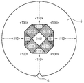
도 2는 <100>-배향을 가지는 반도체 웨이퍼를 평면도로 예시하고, 도 3은 <110>-배향을 가지는 반도체 웨이퍼의 도면이다.
도 4는 본 발명에 따른 장치를 단면도로 예시한다.
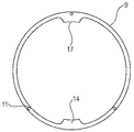
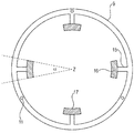
도 5, 도 6 및 도 7은 각각 본 발명에 따른 장치의 특징부인 링을 평면도로 예시한다.
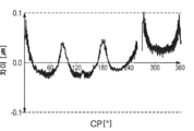
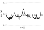
도 8 및 도 9는 각각 둘레 방향 위치(CP)의 함수로서 반도체 웨이퍼의 엣지로부터 1mm 거리의 에피택셜 코팅된 반도체 웨이퍼의 두께와 코팅된 반도체 웨이퍼의 평균 두께 사이의 차이(Diff)를 예시하며, 여기서 에피택셜 층은 기존 방식(도 8) 또는 본 발명에 따른 방식(도 9)으로 증착된 것이다.
2 서셉터 링
3 서셉터 베이스
4 렛지
5 반도체 웨이퍼
6 배향 노치
7 서셉터 유지 샤프트
8 서셉터 유지 아암
9 링
10 서셉터 지지핀
11 구멍
12 웨이퍼 리프팅 샤프트
13 웨이퍼 리프팅 핀
14 돌출부
15 웹
16 링 세그먼트
17 돌출부의 내부 엣지
Claims (7)
- 단결정 재료로 구성된 반도체 웨이퍼의 전면(front side) 상에 에피택셜 층을 증착하는 방법으로서,
반도체 웨이퍼를 제공하는 단계;
상기 반도체 웨이퍼를 서셉터 상에 배치하는 단계;
상기 반도체 웨이퍼의 전면 및 후면으로 유도되는 열복사에 의해 상기 반도체 웨이퍼를 증착 온도로 가열하는 단계;
상기 반도체 웨이퍼의 전면에 걸쳐 증착 가스를 안내하는 단계;
상기 반도체 웨이퍼의 엣지에 있는 제1 부분 영역으로서, 상기 단결정 재료의 배향으로 인해, 상기 반도체 웨이퍼의 온도가 균일한 경우, 인접한 제2 부분 영역에서보다 상기 에피택셜 층의 성장 속도가 더 빠른 것인 제1 부분 영역이 더 약하게 가열되도록, 상기 반도체 웨이퍼의 후면으로 유도되는 열복사의 일부의 강도를 선택적으로 감소시키는 단계
를 포함하는 것을 특징으로 하는 방법. - 제1항에 있어서, 스펙트럼의 IR 범위에서 낮은 투과율을 가지는 재료를 상기 열복사의 빔 경로에 배치하는 것에 의해 상기 열복사의 일부의 강도를 선택적으로 감소시키는 것을 특징으로 하는 방법.
- 단결정 재료로 구성된 반도체 웨이퍼의 전면 상에 에피택셜 층을 증착하는 장치로서,
서셉터;
서셉터 유지 샤프트 및 서셉터 유지 아암을 가지는 서셉터를 유지 및 회전시키는 기구;
상기 서셉터 상에 배치된 반도체 웨이퍼의 엣지에 있는 제1 부분 영역으로서, 상기 단결정 재료의 배향으로 인해, 상기 반도체 웨이퍼의 온도가 균일한 경우, 인접한 제2 부분 영역에서보다 상기 에피택셜 층의 성장 속도가 더 빠른 것인 제1 부분 영역이 더 약하게 가열되도록, 통과되는 열복사의 강도를 선택적으로 감소시키는 내향 돌출부를 구비하고 상기 서셉터 유지 아암에 의해 유지된 링
을 포함하는 것을 특징으로 하는 장치. - 제3항에 있어서, 상기 링은 석영 유리로 구성된 것을 특징으로 하는 장치.
- 제3항 또는 제4항에 있어서, 상기 내향 돌출부는 각각 웹(web) 및 링 세그먼트를 포함하고, 상기 링 세그먼트는 스펙트럼의 IR 범위에서 낮은 투과율을 가지는 재료로 구성되고, 개구 각도(α)로 표현되는 15°이상 25°이하의 둘레 방향 폭을 가지는 것을 특징으로 하는 장치.
- 제3항 내지 제5항 중 어느 항에 있어서,
인접한 돌출부까지의 거리가 90°인 4개의 돌출부
를 포함하는 것을 특징으로 하는 장치. - 제3항 내지 제5항 중 어느 항에 있어서,
인접한 돌출부까지의 거리가 180°인 2개의 돌출부
를 포함하는 것을 특징으로 하는 장치.
Applications Claiming Priority (3)
| Application Number | Priority Date | Filing Date | Title |
|---|---|---|---|
| DE102017222279.4A DE102017222279A1 (de) | 2017-12-08 | 2017-12-08 | Verfahren zum Abscheiden einer epitaktischen Schicht auf einer Vorderseite einer Halbleiterscheibe und Vorrichtung zur Durchführung des Verfahrens |
| DE102017222279.4 | 2017-12-08 | ||
| PCT/EP2018/082820 WO2019110386A1 (de) | 2017-12-08 | 2018-11-28 | Verfahren zum abscheiden einer epitaktischen schicht auf einer vorderseite einer halbleiterscheibe und vorrichtung zur durchführung des verfahrens |
Publications (2)
| Publication Number | Publication Date |
|---|---|
| KR20200084355A true KR20200084355A (ko) | 2020-07-10 |
| KR102370949B1 KR102370949B1 (ko) | 2022-03-08 |
Family
ID=64556919
Family Applications (1)
| Application Number | Title | Priority Date | Filing Date |
|---|---|---|---|
| KR1020207017835A Active KR102370949B1 (ko) | 2017-12-08 | 2018-11-28 | 반도체 웨이퍼의 전면에 에피택셜 층을 증착하는 방법 및 이 방법을 수행하기 위한 장치 |
Country Status (10)
| Country | Link |
|---|---|
| US (1) | US11538683B2 (ko) |
| EP (1) | EP3721469B1 (ko) |
| JP (1) | JP7026795B2 (ko) |
| KR (1) | KR102370949B1 (ko) |
| CN (1) | CN111433891B (ko) |
| DE (1) | DE102017222279A1 (ko) |
| IL (1) | IL275116B2 (ko) |
| SG (1) | SG11202005075RA (ko) |
| TW (1) | TWI704253B (ko) |
| WO (1) | WO2019110386A1 (ko) |
Families Citing this family (9)
| Publication number | Priority date | Publication date | Assignee | Title |
|---|---|---|---|---|
| DE102019207772A1 (de) * | 2019-05-28 | 2020-12-03 | Siltronic Ag | Verfahren zum Abscheiden einer epitaktischen Schicht auf einer Vorderseite einer Halbleiterscheibe und Vorrichtung zur Durchführung des Verfahrens |
| EP3835281A1 (de) | 2019-12-13 | 2021-06-16 | Siltronic AG | Verfahren zur herstellung eines plattenförmigen formkörpers mit einer siliziumkarbid-matrix |
| CN110981172A (zh) * | 2019-12-21 | 2020-04-10 | 张忠恕 | 一种外延工艺石英焊件组件及其加工工艺 |
| CN112501688B (zh) * | 2020-10-30 | 2022-03-15 | 松山湖材料实验室 | 用于生长大尺寸外延片的石墨盘及其使用方法 |
| EP3996130B1 (de) * | 2020-11-09 | 2023-03-08 | Siltronic AG | Verfahren zum abscheiden einer epitaktischen schicht auf einer substratscheibe |
| CN115161623A (zh) | 2021-03-18 | 2022-10-11 | Asm Ip私人控股有限公司 | 用于膜沉积期间衬底温度控制的双高温计系统 |
| KR20220130621A (ko) | 2021-03-18 | 2022-09-27 | 에이에스엠 아이피 홀딩 비.브이. | 램프 뱅크 정렬을 갖는 웨이퍼 외곽 에지 온도 측정 시스템 |
| CN115233191A (zh) * | 2022-08-03 | 2022-10-25 | 拓荆科技股份有限公司 | 一种反应腔及镀膜设备 |
| JP1746404S (ja) * | 2023-01-11 | 2023-06-15 | サセプタカバーベース |
Citations (4)
| Publication number | Priority date | Publication date | Assignee | Title |
|---|---|---|---|---|
| US20070227441A1 (en) * | 2006-03-30 | 2007-10-04 | Kazuhiro Narahara | Method of manufacturing epitaxial silicon wafer and apparatus thereof |
| WO2011075563A2 (en) * | 2009-12-18 | 2011-06-23 | Applied Materials, Inc. | Substrate processing apparatus having a radiant cavity |
| WO2013155073A1 (en) * | 2012-04-10 | 2013-10-17 | Memc Electronic Materials, Inc. | Susceptor for improved epitaxial wafer flatness and methods for fabricating a semiconductor wafer processing device |
| US20150275395A1 (en) * | 2012-10-16 | 2015-10-01 | Lg Siltron Inc. | Susceptor for epitaxial growing and method for epitaxial growing |
Family Cites Families (15)
| Publication number | Priority date | Publication date | Assignee | Title |
|---|---|---|---|---|
| RU2099808C1 (ru) * | 1996-04-01 | 1997-12-20 | Евгений Инвиевич Гиваргизов | Способ выращивания ориентированных систем нитевидных кристаллов и устройство для его осуществления (варианты) |
| JP2001010894A (ja) | 1999-06-24 | 2001-01-16 | Mitsubishi Materials Silicon Corp | 結晶成長用サセプタとこれを用いた結晶成長装置、およびエピタキシャル・ウェーハとその製造方法 |
| JP2002164300A (ja) * | 2000-11-29 | 2002-06-07 | Shin Etsu Handotai Co Ltd | 半導体ウェーハの製造方法 |
| JP2007251078A (ja) * | 2006-03-20 | 2007-09-27 | Nuflare Technology Inc | 気相成長装置 |
| JP4868522B2 (ja) * | 2006-03-30 | 2012-02-01 | Sumco Techxiv株式会社 | エピタキシャルウェーハの製造方法及び製造装置 |
| DE102006055038B4 (de) | 2006-11-22 | 2012-12-27 | Siltronic Ag | Epitaxierte Halbleiterscheibe sowie Vorrichtung und Verfahren zur Herstellung einer epitaxierten Halbleiterscheibe |
| JP2009088088A (ja) * | 2007-09-28 | 2009-04-23 | Sharp Corp | 基板処理装置および基板処理方法 |
| JP5254295B2 (ja) * | 2010-09-22 | 2013-08-07 | 株式会社東芝 | 成膜装置 |
| DE102011083245B4 (de) * | 2011-09-22 | 2019-04-25 | Siltronic Ag | Verfahren und Vorrichtung zum Abscheiden einer epitaktischen Schicht aus Silizium auf einer Halbleiterscheibe aus einkristallinem Silizium durch Gasphasenabscheidung in einer Prozesskammer |
| US9401271B2 (en) * | 2012-04-19 | 2016-07-26 | Sunedison Semiconductor Limited (Uen201334164H) | Susceptor assemblies for supporting wafers in a reactor apparatus |
| JP6035982B2 (ja) | 2012-08-09 | 2016-11-30 | 株式会社Sumco | エピタキシャルシリコンウェーハの製造方法およびエピタキシャルシリコンウェーハ |
| US9123765B2 (en) | 2013-03-11 | 2015-09-01 | Applied Materials, Inc. | Susceptor support shaft for improved wafer temperature uniformity and process repeatability |
| JP6115445B2 (ja) | 2013-10-24 | 2017-04-19 | 信越半導体株式会社 | エピタキシャル成長装置 |
| JP6438330B2 (ja) * | 2015-03-16 | 2018-12-12 | 株式会社Screenホールディングス | 熱処理装置 |
| DE102016210203B3 (de) | 2016-06-09 | 2017-08-31 | Siltronic Ag | Suszeptor zum Halten einer Halbleiterscheibe, Verfahren zum Abscheiden einer epitaktischen Schicht auf einer Vorderseite einer Halbleiterscheibe und Halbleiterscheibe mit epitaktischer Schicht |
-
2017
- 2017-12-08 DE DE102017222279.4A patent/DE102017222279A1/de not_active Withdrawn
-
2018
- 2018-11-26 TW TW107142039A patent/TWI704253B/zh active
- 2018-11-28 IL IL275116A patent/IL275116B2/en unknown
- 2018-11-28 WO PCT/EP2018/082820 patent/WO2019110386A1/de not_active Ceased
- 2018-11-28 EP EP18811247.8A patent/EP3721469B1/de active Active
- 2018-11-28 SG SG11202005075RA patent/SG11202005075RA/en unknown
- 2018-11-28 JP JP2020530995A patent/JP7026795B2/ja active Active
- 2018-11-28 CN CN201880079351.2A patent/CN111433891B/zh active Active
- 2018-11-28 KR KR1020207017835A patent/KR102370949B1/ko active Active
- 2018-11-28 US US16/765,479 patent/US11538683B2/en active Active
Patent Citations (4)
| Publication number | Priority date | Publication date | Assignee | Title |
|---|---|---|---|---|
| US20070227441A1 (en) * | 2006-03-30 | 2007-10-04 | Kazuhiro Narahara | Method of manufacturing epitaxial silicon wafer and apparatus thereof |
| WO2011075563A2 (en) * | 2009-12-18 | 2011-06-23 | Applied Materials, Inc. | Substrate processing apparatus having a radiant cavity |
| WO2013155073A1 (en) * | 2012-04-10 | 2013-10-17 | Memc Electronic Materials, Inc. | Susceptor for improved epitaxial wafer flatness and methods for fabricating a semiconductor wafer processing device |
| US20150275395A1 (en) * | 2012-10-16 | 2015-10-01 | Lg Siltron Inc. | Susceptor for epitaxial growing and method for epitaxial growing |
Also Published As
| Publication number | Publication date |
|---|---|
| US11538683B2 (en) | 2022-12-27 |
| IL275116B (en) | 2022-12-01 |
| US20200294794A1 (en) | 2020-09-17 |
| EP3721469A1 (de) | 2020-10-14 |
| EP3721469B1 (de) | 2026-03-18 |
| CN111433891A (zh) | 2020-07-17 |
| KR102370949B1 (ko) | 2022-03-08 |
| TW201936982A (zh) | 2019-09-16 |
| SG11202005075RA (en) | 2020-06-29 |
| IL275116A (en) | 2020-09-30 |
| JP7026795B2 (ja) | 2022-02-28 |
| IL275116B2 (en) | 2023-04-01 |
| DE102017222279A1 (de) | 2019-06-13 |
| CN111433891B (zh) | 2023-06-02 |
| WO2019110386A1 (de) | 2019-06-13 |
| TWI704253B (zh) | 2020-09-11 |
| JP2021506125A (ja) | 2021-02-18 |
Similar Documents
| Publication | Publication Date | Title |
|---|---|---|
| KR102370949B1 (ko) | 반도체 웨이퍼의 전면에 에피택셜 층을 증착하는 방법 및 이 방법을 수행하기 위한 장치 | |
| TWI649781B (zh) | 用於化學氣相沈積之自定中心晶圓載具系統 | |
| TWI488258B (zh) | 增強之晶圓載體 | |
| US20050092439A1 (en) | Low/high temperature substrate holder to reduce edge rolloff and backside damage | |
| EP3863043A1 (en) | Susceptor | |
| KR20130037688A (ko) | 열 특징부를 갖는 웨이퍼 캐리어 | |
| KR20120118416A (ko) | 공정 가스에서 발생된 재료 층을 기판 웨이퍼상에 증착하는 방법 및 장치 | |
| JP7532417B2 (ja) | ウェハの表面にエピタキシャル層を堆積させる方法、およびこの方法を実施するための装置 | |
| US20190106809A1 (en) | Susceptor for holding a semiconductor wafer, method for depositing an epitaxial layer on a front side of a semiconductor wafer, and semiconductor wafer with epitaxial layer | |
| JP3004846B2 (ja) | 気相成長装置用サセプタ | |
| JP3596710B2 (ja) | 気相成長装置用サセプタ | |
| JP7828348B2 (ja) | 半導体ウエハリアクタ中の輻射熱キャップのためのシステムと方法 | |
| KR102335880B1 (ko) | 반도체 웨이퍼의 정면 상에 층의 성막 중에 방위 노치를 갖는 반도체 웨이퍼를 유지하는 서셉터, 및 이 서셉터를 사용하여 층을 성막하는 방법 | |
| US3419424A (en) | Method of influencing the surface profile of semiconductor layers precipitated from the gas phase | |
| JP2008091615A (ja) | 被加工処理基板、その製造方法およびその加工処理方法 | |
| KR20110087440A (ko) | 반도체 제조용 서셉터 및 이를 포함하는 반도체 제조 장치 | |
| KR102622605B1 (ko) | 서셉터 및 반도체 제조장치 | |
| JP2004172392A (ja) | 半導体エピタキシャルウェーハの製造装置およびサセプタ並びにサセプタの支持装置 | |
| KR20150093495A (ko) | 반도체 제조 장치 | |
| KR20180092673A (ko) | 대구경 웨이퍼용 웨이퍼 캐리어 |
Legal Events
| Date | Code | Title | Description |
|---|---|---|---|
| PA0105 | International application |
St.27 status event code: A-0-1-A10-A15-nap-PA0105 |
|
| PA0201 | Request for examination |
St.27 status event code: A-1-2-D10-D11-exm-PA0201 |
|
| P11-X000 | Amendment of application requested |
St.27 status event code: A-2-2-P10-P11-nap-X000 |
|
| P13-X000 | Application amended |
St.27 status event code: A-2-2-P10-P13-nap-X000 |
|
| PG1501 | Laying open of application |
St.27 status event code: A-1-1-Q10-Q12-nap-PG1501 |
|
| R18-X000 | Changes to party contact information recorded |
St.27 status event code: A-3-3-R10-R18-oth-X000 |
|
| E902 | Notification of reason for refusal | ||
| PE0902 | Notice of grounds for rejection |
St.27 status event code: A-1-2-D10-D21-exm-PE0902 |
|
| E13-X000 | Pre-grant limitation requested |
St.27 status event code: A-2-3-E10-E13-lim-X000 |
|
| P11-X000 | Amendment of application requested |
St.27 status event code: A-2-2-P10-P11-nap-X000 |
|
| P13-X000 | Application amended |
St.27 status event code: A-2-2-P10-P13-nap-X000 |
|
| E701 | Decision to grant or registration of patent right | ||
| PE0701 | Decision of registration |
St.27 status event code: A-1-2-D10-D22-exm-PE0701 |
|
| GRNT | Written decision to grant | ||
| PR0701 | Registration of establishment |
St.27 status event code: A-2-4-F10-F11-exm-PR0701 |
|
| PR1002 | Payment of registration fee |
St.27 status event code: A-2-2-U10-U12-oth-PR1002 Fee payment year number: 1 |
|
| PG1601 | Publication of registration |
St.27 status event code: A-4-4-Q10-Q13-nap-PG1601 |
|
| P22-X000 | Classification modified |
St.27 status event code: A-4-4-P10-P22-nap-X000 |
|
| PR1001 | Payment of annual fee |
St.27 status event code: A-4-4-U10-U11-oth-PR1001 Fee payment year number: 4 |
|
| U11 | Full renewal or maintenance fee paid |
Free format text: ST27 STATUS EVENT CODE: A-4-4-U10-U11-OTH-PR1001 (AS PROVIDED BY THE NATIONAL OFFICE) Year of fee payment: 4 |