KR20200087155A - 광학 부재 - Google Patents
광학 부재 Download PDFInfo
- Publication number
- KR20200087155A KR20200087155A KR1020207013877A KR20207013877A KR20200087155A KR 20200087155 A KR20200087155 A KR 20200087155A KR 1020207013877 A KR1020207013877 A KR 1020207013877A KR 20207013877 A KR20207013877 A KR 20207013877A KR 20200087155 A KR20200087155 A KR 20200087155A
- Authority
- KR
- South Korea
- Prior art keywords
- adhesive layer
- light
- meth
- optical member
- optical
- Prior art date
- Legal status (The legal status is an assumption and is not a legal conclusion. Google has not performed a legal analysis and makes no representation as to the accuracy of the status listed.)
- Granted
Links
Images


Classifications
-
- G—PHYSICS
- G02—OPTICS
- G02B—OPTICAL ELEMENTS, SYSTEMS OR APPARATUS
- G02B6/00—Light guides; Structural details of arrangements comprising light guides and other optical elements, e.g. couplings
- G02B6/0001—Light guides; Structural details of arrangements comprising light guides and other optical elements, e.g. couplings specially adapted for lighting devices or systems
- G02B6/0011—Light guides; Structural details of arrangements comprising light guides and other optical elements, e.g. couplings specially adapted for lighting devices or systems the light guides being planar or of plate-like form
- G02B6/0033—Means for improving the coupling-out of light from the light guide
- G02B6/005—Means for improving the coupling-out of light from the light guide provided by one optical element, or plurality thereof, placed on the light output side of the light guide
-
- G—PHYSICS
- G02—OPTICS
- G02B—OPTICAL ELEMENTS, SYSTEMS OR APPARATUS
- G02B5/00—Optical elements other than lenses
- G02B5/02—Diffusing elements; Afocal elements
-
- G—PHYSICS
- G02—OPTICS
- G02B—OPTICAL ELEMENTS, SYSTEMS OR APPARATUS
- G02B5/00—Optical elements other than lenses
- G02B5/02—Diffusing elements; Afocal elements
- G02B5/0205—Diffusing elements; Afocal elements characterised by the diffusing properties
- G02B5/021—Diffusing elements; Afocal elements characterised by the diffusing properties the diffusion taking place at the element's surface, e.g. by means of surface roughening or microprismatic structures
- G02B5/0221—Diffusing elements; Afocal elements characterised by the diffusing properties the diffusion taking place at the element's surface, e.g. by means of surface roughening or microprismatic structures the surface having an irregular structure
-
- G—PHYSICS
- G02—OPTICS
- G02B—OPTICAL ELEMENTS, SYSTEMS OR APPARATUS
- G02B5/00—Optical elements other than lenses
- G02B5/02—Diffusing elements; Afocal elements
- G02B5/0205—Diffusing elements; Afocal elements characterised by the diffusing properties
- G02B5/021—Diffusing elements; Afocal elements characterised by the diffusing properties the diffusion taking place at the element's surface, e.g. by means of surface roughening or microprismatic structures
- G02B5/0231—Diffusing elements; Afocal elements characterised by the diffusing properties the diffusion taking place at the element's surface, e.g. by means of surface roughening or microprismatic structures the surface having microprismatic or micropyramidal shape
-
- G—PHYSICS
- G02—OPTICS
- G02B—OPTICAL ELEMENTS, SYSTEMS OR APPARATUS
- G02B5/00—Optical elements other than lenses
- G02B5/02—Diffusing elements; Afocal elements
- G02B5/0273—Diffusing elements; Afocal elements characterized by the use
- G02B5/0278—Diffusing elements; Afocal elements characterized by the use used in transmission
-
- G—PHYSICS
- G02—OPTICS
- G02B—OPTICAL ELEMENTS, SYSTEMS OR APPARATUS
- G02B5/00—Optical elements other than lenses
- G02B5/12—Reflex reflectors
-
- G—PHYSICS
- G02—OPTICS
- G02B—OPTICAL ELEMENTS, SYSTEMS OR APPARATUS
- G02B7/00—Mountings, adjusting means, or light-tight connections, for optical elements
-
- G—PHYSICS
- G02—OPTICS
- G02F—OPTICAL DEVICES OR ARRANGEMENTS FOR THE CONTROL OF LIGHT BY MODIFICATION OF THE OPTICAL PROPERTIES OF THE MEDIA OF THE ELEMENTS INVOLVED THEREIN; NON-LINEAR OPTICS; FREQUENCY-CHANGING OF LIGHT; OPTICAL LOGIC ELEMENTS; OPTICAL ANALOGUE/DIGITAL CONVERTERS
- G02F1/00—Devices or arrangements for the control of the intensity, colour, phase, polarisation or direction of light arriving from an independent light source, e.g. switching, gating or modulating; Non-linear optics
- G02F1/01—Devices or arrangements for the control of the intensity, colour, phase, polarisation or direction of light arriving from an independent light source, e.g. switching, gating or modulating; Non-linear optics for the control of the intensity, phase, polarisation or colour
- G02F1/13—Devices or arrangements for the control of the intensity, colour, phase, polarisation or direction of light arriving from an independent light source, e.g. switching, gating or modulating; Non-linear optics for the control of the intensity, phase, polarisation or colour based on liquid crystals, e.g. single liquid crystal display cells
- G02F1/133—Constructional arrangements; Operation of liquid crystal cells; Circuit arrangements
- G02F1/1333—Constructional arrangements; Manufacturing methods
- G02F1/1335—Structural association of cells with optical devices, e.g. polarisers or reflectors
-
- G—PHYSICS
- G02—OPTICS
- G02F—OPTICAL DEVICES OR ARRANGEMENTS FOR THE CONTROL OF LIGHT BY MODIFICATION OF THE OPTICAL PROPERTIES OF THE MEDIA OF THE ELEMENTS INVOLVED THEREIN; NON-LINEAR OPTICS; FREQUENCY-CHANGING OF LIGHT; OPTICAL LOGIC ELEMENTS; OPTICAL ANALOGUE/DIGITAL CONVERTERS
- G02F1/00—Devices or arrangements for the control of the intensity, colour, phase, polarisation or direction of light arriving from an independent light source, e.g. switching, gating or modulating; Non-linear optics
- G02F1/01—Devices or arrangements for the control of the intensity, colour, phase, polarisation or direction of light arriving from an independent light source, e.g. switching, gating or modulating; Non-linear optics for the control of the intensity, phase, polarisation or colour
- G02F1/13—Devices or arrangements for the control of the intensity, colour, phase, polarisation or direction of light arriving from an independent light source, e.g. switching, gating or modulating; Non-linear optics for the control of the intensity, phase, polarisation or colour based on liquid crystals, e.g. single liquid crystal display cells
- G02F1/133—Constructional arrangements; Operation of liquid crystal cells; Circuit arrangements
- G02F1/1333—Constructional arrangements; Manufacturing methods
- G02F1/1335—Structural association of cells with optical devices, e.g. polarisers or reflectors
- G02F1/133504—Diffusing, scattering, diffracting elements
-
- G—PHYSICS
- G02—OPTICS
- G02F—OPTICAL DEVICES OR ARRANGEMENTS FOR THE CONTROL OF LIGHT BY MODIFICATION OF THE OPTICAL PROPERTIES OF THE MEDIA OF THE ELEMENTS INVOLVED THEREIN; NON-LINEAR OPTICS; FREQUENCY-CHANGING OF LIGHT; OPTICAL LOGIC ELEMENTS; OPTICAL ANALOGUE/DIGITAL CONVERTERS
- G02F1/00—Devices or arrangements for the control of the intensity, colour, phase, polarisation or direction of light arriving from an independent light source, e.g. switching, gating or modulating; Non-linear optics
- G02F1/01—Devices or arrangements for the control of the intensity, colour, phase, polarisation or direction of light arriving from an independent light source, e.g. switching, gating or modulating; Non-linear optics for the control of the intensity, phase, polarisation or colour
- G02F1/13—Devices or arrangements for the control of the intensity, colour, phase, polarisation or direction of light arriving from an independent light source, e.g. switching, gating or modulating; Non-linear optics for the control of the intensity, phase, polarisation or colour based on liquid crystals, e.g. single liquid crystal display cells
- G02F1/133—Constructional arrangements; Operation of liquid crystal cells; Circuit arrangements
- G02F1/1333—Constructional arrangements; Manufacturing methods
- G02F1/1335—Structural association of cells with optical devices, e.g. polarisers or reflectors
- G02F1/133504—Diffusing, scattering, diffracting elements
- G02F1/133507—Films for enhancing the luminance
-
- G—PHYSICS
- G02—OPTICS
- G02F—OPTICAL DEVICES OR ARRANGEMENTS FOR THE CONTROL OF LIGHT BY MODIFICATION OF THE OPTICAL PROPERTIES OF THE MEDIA OF THE ELEMENTS INVOLVED THEREIN; NON-LINEAR OPTICS; FREQUENCY-CHANGING OF LIGHT; OPTICAL LOGIC ELEMENTS; OPTICAL ANALOGUE/DIGITAL CONVERTERS
- G02F1/00—Devices or arrangements for the control of the intensity, colour, phase, polarisation or direction of light arriving from an independent light source, e.g. switching, gating or modulating; Non-linear optics
- G02F1/01—Devices or arrangements for the control of the intensity, colour, phase, polarisation or direction of light arriving from an independent light source, e.g. switching, gating or modulating; Non-linear optics for the control of the intensity, phase, polarisation or colour
- G02F1/13—Devices or arrangements for the control of the intensity, colour, phase, polarisation or direction of light arriving from an independent light source, e.g. switching, gating or modulating; Non-linear optics for the control of the intensity, phase, polarisation or colour based on liquid crystals, e.g. single liquid crystal display cells
- G02F1/133—Constructional arrangements; Operation of liquid crystal cells; Circuit arrangements
- G02F1/1333—Constructional arrangements; Manufacturing methods
- G02F1/1335—Structural association of cells with optical devices, e.g. polarisers or reflectors
- G02F1/133528—Polarisers
- G02F1/133531—Polarisers characterised by the arrangement of polariser or analyser axes
-
- G—PHYSICS
- G02—OPTICS
- G02F—OPTICAL DEVICES OR ARRANGEMENTS FOR THE CONTROL OF LIGHT BY MODIFICATION OF THE OPTICAL PROPERTIES OF THE MEDIA OF THE ELEMENTS INVOLVED THEREIN; NON-LINEAR OPTICS; FREQUENCY-CHANGING OF LIGHT; OPTICAL LOGIC ELEMENTS; OPTICAL ANALOGUE/DIGITAL CONVERTERS
- G02F1/00—Devices or arrangements for the control of the intensity, colour, phase, polarisation or direction of light arriving from an independent light source, e.g. switching, gating or modulating; Non-linear optics
- G02F1/01—Devices or arrangements for the control of the intensity, colour, phase, polarisation or direction of light arriving from an independent light source, e.g. switching, gating or modulating; Non-linear optics for the control of the intensity, phase, polarisation or colour
- G02F1/13—Devices or arrangements for the control of the intensity, colour, phase, polarisation or direction of light arriving from an independent light source, e.g. switching, gating or modulating; Non-linear optics for the control of the intensity, phase, polarisation or colour based on liquid crystals, e.g. single liquid crystal display cells
- G02F1/133—Constructional arrangements; Operation of liquid crystal cells; Circuit arrangements
- G02F1/1333—Constructional arrangements; Manufacturing methods
- G02F1/1335—Structural association of cells with optical devices, e.g. polarisers or reflectors
- G02F1/133528—Polarisers
- G02F1/133536—Reflective polarizers
-
- G—PHYSICS
- G02—OPTICS
- G02F—OPTICAL DEVICES OR ARRANGEMENTS FOR THE CONTROL OF LIGHT BY MODIFICATION OF THE OPTICAL PROPERTIES OF THE MEDIA OF THE ELEMENTS INVOLVED THEREIN; NON-LINEAR OPTICS; FREQUENCY-CHANGING OF LIGHT; OPTICAL LOGIC ELEMENTS; OPTICAL ANALOGUE/DIGITAL CONVERTERS
- G02F2202/00—Materials and properties
- G02F2202/28—Adhesive materials or arrangements
-
- G—PHYSICS
- G02—OPTICS
- G02F—OPTICAL DEVICES OR ARRANGEMENTS FOR THE CONTROL OF LIGHT BY MODIFICATION OF THE OPTICAL PROPERTIES OF THE MEDIA OF THE ELEMENTS INVOLVED THEREIN; NON-LINEAR OPTICS; FREQUENCY-CHANGING OF LIGHT; OPTICAL LOGIC ELEMENTS; OPTICAL ANALOGUE/DIGITAL CONVERTERS
- G02F2202/00—Materials and properties
- G02F2202/36—Micro- or nanomaterials
Landscapes
- Physics & Mathematics (AREA)
- General Physics & Mathematics (AREA)
- Optics & Photonics (AREA)
- Nonlinear Science (AREA)
- Mathematical Physics (AREA)
- Chemical & Material Sciences (AREA)
- Crystallography & Structural Chemistry (AREA)
- Liquid Crystal (AREA)
- Optical Elements Other Than Lenses (AREA)
- Mounting And Adjusting Of Optical Elements (AREA)
- Glass Compositions (AREA)
Abstract
Description
도 2 는, 본 발명의 실시형태에 사용될 수 있는 접착층의 공극부의 평면에서 본 형상의 예를 설명하는 개략 평면도이다.
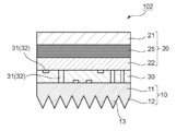
도 3 은, 본 발명의 다른 실시형태에 의한 광학 부재를 설명하는 개략 단면도이다.
도 4 는, 본 발명의 또 다른 실시형태에 의한 광학 부재를 설명하는 개략 단면도이다.
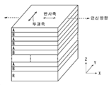
도 5 는, 본 발명의 광학 부재의 제 2 부재로서 사용될 수 있는 반사형 편광자의 일례의 개략 사시도이다.

20 : 제 2 부재
30 : 접착층
100 : 광학 부재
101 : 광학 부재
102 : 광학 부재
Claims (8)
- 광의 방향 변환 기능을 갖는 제 1 부재와, 그 제 1 부재에 접착층을 개재하여 적층된 제 2 부재를 갖고,
그 접착층이 공극부를 가지며, 그 접착층과 그 제 1 부재 및/또는 제 2 부재의 계면에 비접촉부가 규정되어 있고,
그 접착층과 그 제 1 부재 및 그 제 2 부재가, 평면에서 본 경우의 4 개의 모퉁이부에 있어서 접촉하고 있는, 광학 부재. - 제 1 항에 있어서,
상기 접착층과 상기 제 1 부재 및 상기 제 2 부재가, 평면에서 본 경우의 둘레 가장자리부 전체에 걸쳐서 접촉하고 있는, 광학 부재. - 제 1 항 또는 제 2 항에 있어서,
상기 접착층의 공극부가, 그 접착층의 표면 요철 구조의 오목부에 의해 규정되어 있는, 광학 부재. - 제 1 항 내지 제 3 항 중 어느 한 항에 있어서,
상기 접착층의 공극부가, 그 접착층의 두께 방향으로 관통된 관통공을 포함하는, 광학 부재. - 제 1 항 내지 제 4 항 중 어느 한 항에 있어서,
상기 접착층을 평면에서 본 경우의 공극률이 70 % ∼ 90 % 인, 광학 부재. - 제 1 항 내지 제 5 항 중 어느 한 항에 있어서,
상기 제 2 부재의 상기 제 1 부재와 반대측에, 확산판을 추가로 갖는, 광학 부재. - 제 6 항에 있어서,
상기 확산판이, 상기 제 2 부재로부터 이간하여 배치되어 있는, 광학 부재. - 제 1 항 내지 제 5 항 중 어느 한 항에 있어서,
상기 제 2 부재가, 다른 접착층을 개재하여 적층된 2 개의 광학 필름의 적층체이고, 그 다른 접착층이 광 확산성을 갖는, 광학 부재.
Applications Claiming Priority (3)
| Application Number | Priority Date | Filing Date | Title |
|---|---|---|---|
| JP2017221172A JP6993187B2 (ja) | 2017-11-16 | 2017-11-16 | 光学部材 |
| JPJP-P-2017-221172 | 2017-11-16 | ||
| PCT/JP2018/038411 WO2019097930A1 (ja) | 2017-11-16 | 2018-10-16 | 光学部材 |
Publications (2)
| Publication Number | Publication Date |
|---|---|
| KR20200087155A true KR20200087155A (ko) | 2020-07-20 |
| KR102655465B1 KR102655465B1 (ko) | 2024-04-09 |
Family
ID=66538942
Family Applications (1)
| Application Number | Title | Priority Date | Filing Date |
|---|---|---|---|
| KR1020207013877A Active KR102655465B1 (ko) | 2017-11-16 | 2018-10-16 | 광학 부재 |
Country Status (7)
| Country | Link |
|---|---|
| US (1) | US11112640B2 (ko) |
| EP (1) | EP3712662A4 (ko) |
| JP (1) | JP6993187B2 (ko) |
| KR (1) | KR102655465B1 (ko) |
| CN (1) | CN111356944A (ko) |
| TW (1) | TWI802611B (ko) |
| WO (1) | WO2019097930A1 (ko) |
Families Citing this family (2)
| Publication number | Priority date | Publication date | Assignee | Title |
|---|---|---|---|---|
| JP7686565B2 (ja) * | 2019-09-30 | 2025-06-02 | 日東電工株式会社 | 偏光板のセットおよび該セットを含む画像表示装置 |
| KR102819945B1 (ko) | 2019-10-08 | 2025-06-13 | 주식회사 브이씨 | 홀 위치 업데이트 장치, 홀 위치 업데이트 시스템 및 홀 커터 |
Citations (4)
| Publication number | Priority date | Publication date | Assignee | Title |
|---|---|---|---|---|
| JPS5346066U (ko) | 1976-09-24 | 1978-04-19 | ||
| JP2003084137A (ja) * | 2001-07-02 | 2003-03-19 | Sumitomo Chem Co Ltd | 半透過半反射性偏光素子及びそれの光学装置への適用 |
| CN1656395A (zh) * | 2002-05-28 | 2005-08-17 | 3M创新有限公司 | 多功能光学组件 |
| JP2017090578A (ja) * | 2015-11-05 | 2017-05-25 | サンテックオプト株式会社 | 額縁状の封し部を有する積層光学フィルムシート |
Family Cites Families (26)
| Publication number | Priority date | Publication date | Assignee | Title |
|---|---|---|---|---|
| JPS5346066B2 (ko) | 1972-04-14 | 1978-12-11 | ||
| JP3042842B2 (ja) | 1987-11-12 | 2000-05-22 | 三菱レイヨン株式会社 | 面光源素子 |
| KR100344364B1 (ko) | 1993-12-21 | 2002-11-30 | 미네소타 마이닝 앤드 매뉴팩춰링 캄파니 | 광학편광자및디스플레이장치 |
| WO2001037007A1 (en) | 1999-11-12 | 2001-05-25 | Kaneka Corporation | Transparent film |
| JP2001343529A (ja) | 2000-03-30 | 2001-12-14 | Kanegafuchi Chem Ind Co Ltd | 偏光子保護フィルムおよびその製造方法 |
| JP2003215570A (ja) * | 2002-01-22 | 2003-07-30 | Sumitomo Chem Co Ltd | 半透過半反射型液晶表示装置とそれ用の光源装置及びフィルム |
| TW557371B (en) * | 2001-07-02 | 2003-10-11 | Sumitomo Chemical Co | Semi-transparent-semi-reflectivity film, semi- transparent-semi-reflectivity polarized film, polarized light device using these films, and liquid crystal display device using these films |
| US6846089B2 (en) | 2003-05-16 | 2005-01-25 | 3M Innovative Properties Company | Method for stacking surface structured optical films |
| US7497973B2 (en) | 2005-02-02 | 2009-03-03 | Lumination Llc | Red line emitting phosphor materials for use in LED applications |
| EP2463354B1 (en) | 2005-12-08 | 2017-03-29 | National Institute for Materials Science | Phosphor, Process for producing the same, and luminescent device |
| US7924368B2 (en) * | 2005-12-08 | 2011-04-12 | 3M Innovative Properties Company | Diffuse multilayer optical assembly |
| JP2007294465A (ja) * | 2007-05-17 | 2007-11-08 | Epson Imaging Devices Corp | 照明装置、電気光学装置及び電子機器 |
| JP2010533976A (ja) | 2007-07-18 | 2010-10-28 | キユーデイー・ビジヨン・インコーポレーテツド | 固体照明に有用な量子ドットベースの光シート |
| JP5157294B2 (ja) | 2007-07-24 | 2013-03-06 | 凸版印刷株式会社 | レンズシート、ディスプレイ用光学シート及びそれを用いたバックライトユニット、ディスプレイ装置 |
| JP5104459B2 (ja) | 2008-03-27 | 2012-12-19 | 凸版印刷株式会社 | 光学部材とそれを用いたバックライト・ユニット、ディスプレイ |
| US8870436B2 (en) * | 2008-09-17 | 2014-10-28 | 3M Innovative Properties Company | Patterned adhesives for reflectors |
| JP5529665B2 (ja) * | 2009-11-16 | 2014-06-25 | 住友化学株式会社 | 偏光板、ならびにこれを用いた液晶パネルおよび液晶表示装置 |
| JP5414738B2 (ja) | 2010-09-03 | 2014-02-12 | 日東電工株式会社 | 薄型偏光膜の製造方法 |
| EP2638321B1 (en) | 2010-11-10 | 2019-05-08 | Nanosys, Inc. | Quantum dot films, lighting devices, and lighting methods |
| KR20120092322A (ko) | 2011-02-11 | 2012-08-21 | 엘지이노텍 주식회사 | 표시장치 |
| JP5812444B2 (ja) * | 2012-04-13 | 2015-11-11 | 日東電工株式会社 | 光学部材、偏光板のセットおよび液晶表示装置 |
| JP6230974B2 (ja) | 2013-08-26 | 2017-11-15 | 富士フイルム株式会社 | 光変換部材、バックライトユニット、および液晶表示装置、ならびに光変換部材の製造方法 |
| JP2015102857A (ja) | 2013-11-28 | 2015-06-04 | 富士フイルム株式会社 | 光変換部材、バックライトユニット、および液晶表示装置、ならびに光変換部材の製造方法 |
| KR20180036999A (ko) * | 2015-08-05 | 2018-04-10 | 쓰리엠 이노베이티브 프로퍼티즈 컴파니 | 광학 확산 필름 라미네이트 및 제조 방법 |
| JP6829969B2 (ja) | 2015-09-28 | 2021-02-17 | 日東電工株式会社 | 光学部材、ならびに、該光学部材を用いた偏光板のセットおよび液晶表示装置 |
| KR102679539B1 (ko) * | 2016-12-06 | 2024-06-28 | 삼성디스플레이 주식회사 | 표시 장치 |
-
2017
- 2017-11-16 JP JP2017221172A patent/JP6993187B2/ja active Active
-
2018
- 2018-10-16 WO PCT/JP2018/038411 patent/WO2019097930A1/ja not_active Ceased
- 2018-10-16 KR KR1020207013877A patent/KR102655465B1/ko active Active
- 2018-10-16 EP EP18877848.4A patent/EP3712662A4/en not_active Withdrawn
- 2018-10-16 CN CN201880074298.7A patent/CN111356944A/zh active Pending
- 2018-10-16 US US16/764,738 patent/US11112640B2/en not_active Expired - Fee Related
- 2018-11-15 TW TW107140509A patent/TWI802611B/zh active
Patent Citations (4)
| Publication number | Priority date | Publication date | Assignee | Title |
|---|---|---|---|---|
| JPS5346066U (ko) | 1976-09-24 | 1978-04-19 | ||
| JP2003084137A (ja) * | 2001-07-02 | 2003-03-19 | Sumitomo Chem Co Ltd | 半透過半反射性偏光素子及びそれの光学装置への適用 |
| CN1656395A (zh) * | 2002-05-28 | 2005-08-17 | 3M创新有限公司 | 多功能光学组件 |
| JP2017090578A (ja) * | 2015-11-05 | 2017-05-25 | サンテックオプト株式会社 | 額縁状の封し部を有する積層光学フィルムシート |
Also Published As
| Publication number | Publication date |
|---|---|
| US20210181570A1 (en) | 2021-06-17 |
| WO2019097930A1 (ja) | 2019-05-23 |
| KR102655465B1 (ko) | 2024-04-09 |
| US11112640B2 (en) | 2021-09-07 |
| TWI802611B (zh) | 2023-05-21 |
| EP3712662A4 (en) | 2021-08-04 |
| JP2019090970A (ja) | 2019-06-13 |
| TW201923436A (zh) | 2019-06-16 |
| JP6993187B2 (ja) | 2022-01-13 |
| EP3712662A1 (en) | 2020-09-23 |
| CN111356944A (zh) | 2020-06-30 |
Similar Documents
| Publication | Publication Date | Title |
|---|---|---|
| US8619363B1 (en) | Light redirecting element comprising a forward diffracting region and a scattering region | |
| JP6780987B2 (ja) | 光学部材 | |
| JP6872330B2 (ja) | 光学部材、ならびに、該光学部材を用いた偏光板のセットおよび液晶表示装置 | |
| JP6829969B2 (ja) | 光学部材、ならびに、該光学部材を用いた偏光板のセットおよび液晶表示装置 | |
| JP3681343B2 (ja) | 積層光学フィルムとその製造方法及びこれを用いた液晶表示装置 | |
| KR20160105442A (ko) | 시준 반사 편광기를 포함하는 광학 필름 | |
| KR20100103555A (ko) | 프리즘 구조체를 가진 백라이트 반사기 | |
| KR101251702B1 (ko) | 광학 필름 및 이것을 사용한 백라이트 장치 | |
| JP7555394B2 (ja) | 均一な照明のためのバックライト | |
| US11112640B2 (en) | Optical member | |
| KR20180110022A (ko) | 일체형 광학 필름 조립체 | |
| JP2000075136A (ja) | 光拡散偏光板 | |
| JP2000075135A (ja) | 光拡散偏光板 | |
| CN107111037A (zh) | 光学片以及包括其的偏光板和液晶显示器 | |
| KR102543293B1 (ko) | 광학 부재 및 도광 시스템 | |
| KR102315475B1 (ko) | 광학 부재 | |
| JP2000162440A (ja) | 偏光板 | |
| JP5982816B2 (ja) | 有機エレクトロルミネッセンス表示装置 | |
| TW201234056A (en) | Optical sheet | |
| KR102603101B1 (ko) | 적층체, 적층체의 제조 방법, 광학체의 형성 방법 및 카메라 모듈 탑재 장치 | |
| EP3605169A1 (en) | Optical filter and optical communication device |
Legal Events
| Date | Code | Title | Description |
|---|---|---|---|
| PA0105 | International application |
Patent event date: 20200514 Patent event code: PA01051R01D Comment text: International Patent Application |
|
| PG1501 | Laying open of application | ||
| A201 | Request for examination | ||
| PA0201 | Request for examination |
Patent event code: PA02012R01D Patent event date: 20210702 Comment text: Request for Examination of Application |
|
| E902 | Notification of reason for refusal | ||
| PE0902 | Notice of grounds for rejection |
Comment text: Notification of reason for refusal Patent event date: 20230811 Patent event code: PE09021S01D |
|
| E701 | Decision to grant or registration of patent right | ||
| PE0701 | Decision of registration |
Patent event code: PE07011S01D Comment text: Decision to Grant Registration Patent event date: 20240201 |
|
| GRNT | Written decision to grant | ||
| PR0701 | Registration of establishment |
Comment text: Registration of Establishment Patent event date: 20240403 Patent event code: PR07011E01D |
|
| PR1002 | Payment of registration fee |
Payment date: 20240403 End annual number: 3 Start annual number: 1 |
|
| PG1601 | Publication of registration |