KR20200093650A - 표시 장치 - Google Patents
표시 장치 Download PDFInfo
- Publication number
- KR20200093650A KR20200093650A KR1020207019643A KR20207019643A KR20200093650A KR 20200093650 A KR20200093650 A KR 20200093650A KR 1020207019643 A KR1020207019643 A KR 1020207019643A KR 20207019643 A KR20207019643 A KR 20207019643A KR 20200093650 A KR20200093650 A KR 20200093650A
- Authority
- KR
- South Korea
- Prior art keywords
- potential
- transistor
- display device
- electrode
- wiring
- Prior art date
- Legal status (The legal status is an assumption and is not a legal conclusion. Google has not performed a legal analysis and makes no representation as to the accuracy of the status listed.)
- Granted
Links
Images








Classifications
-
- G—PHYSICS
- G09—EDUCATION; CRYPTOGRAPHY; DISPLAY; ADVERTISING; SEALS
- G09G—ARRANGEMENTS OR CIRCUITS FOR CONTROL OF INDICATING DEVICES USING STATIC MEANS TO PRESENT VARIABLE INFORMATION
- G09G3/00—Control arrangements or circuits, of interest only in connection with visual indicators other than cathode-ray tubes
- G09G3/20—Control arrangements or circuits, of interest only in connection with visual indicators other than cathode-ray tubes for presentation of an assembly of a number of characters, e.g. a page, by composing the assembly by combination of individual elements arranged in a matrix no fixed position being assigned to or needed to be assigned to the individual characters or partial characters
- G09G3/34—Control arrangements or circuits, of interest only in connection with visual indicators other than cathode-ray tubes for presentation of an assembly of a number of characters, e.g. a page, by composing the assembly by combination of individual elements arranged in a matrix no fixed position being assigned to or needed to be assigned to the individual characters or partial characters by control of light from an independent source
- G09G3/36—Control arrangements or circuits, of interest only in connection with visual indicators other than cathode-ray tubes for presentation of an assembly of a number of characters, e.g. a page, by composing the assembly by combination of individual elements arranged in a matrix no fixed position being assigned to or needed to be assigned to the individual characters or partial characters by control of light from an independent source using liquid crystals
- G09G3/3611—Control of matrices with row and column drivers
- G09G3/3614—Control of polarity reversal in general
-
- G—PHYSICS
- G02—OPTICS
- G02F—OPTICAL DEVICES OR ARRANGEMENTS FOR THE CONTROL OF LIGHT BY MODIFICATION OF THE OPTICAL PROPERTIES OF THE MEDIA OF THE ELEMENTS INVOLVED THEREIN; NON-LINEAR OPTICS; FREQUENCY-CHANGING OF LIGHT; OPTICAL LOGIC ELEMENTS; OPTICAL ANALOGUE/DIGITAL CONVERTERS
- G02F1/00—Devices or arrangements for the control of the intensity, colour, phase, polarisation or direction of light arriving from an independent light source, e.g. switching, gating or modulating; Non-linear optics
- G02F1/01—Devices or arrangements for the control of the intensity, colour, phase, polarisation or direction of light arriving from an independent light source, e.g. switching, gating or modulating; Non-linear optics for the control of the intensity, phase, polarisation or colour
- G02F1/13—Devices or arrangements for the control of the intensity, colour, phase, polarisation or direction of light arriving from an independent light source, e.g. switching, gating or modulating; Non-linear optics for the control of the intensity, phase, polarisation or colour based on liquid crystals, e.g. single liquid crystal display cells
- G02F1/133—Constructional arrangements; Operation of liquid crystal cells; Circuit arrangements
-
- G—PHYSICS
- G02—OPTICS
- G02F—OPTICAL DEVICES OR ARRANGEMENTS FOR THE CONTROL OF LIGHT BY MODIFICATION OF THE OPTICAL PROPERTIES OF THE MEDIA OF THE ELEMENTS INVOLVED THEREIN; NON-LINEAR OPTICS; FREQUENCY-CHANGING OF LIGHT; OPTICAL LOGIC ELEMENTS; OPTICAL ANALOGUE/DIGITAL CONVERTERS
- G02F1/00—Devices or arrangements for the control of the intensity, colour, phase, polarisation or direction of light arriving from an independent light source, e.g. switching, gating or modulating; Non-linear optics
- G02F1/01—Devices or arrangements for the control of the intensity, colour, phase, polarisation or direction of light arriving from an independent light source, e.g. switching, gating or modulating; Non-linear optics for the control of the intensity, phase, polarisation or colour
- G02F1/13—Devices or arrangements for the control of the intensity, colour, phase, polarisation or direction of light arriving from an independent light source, e.g. switching, gating or modulating; Non-linear optics for the control of the intensity, phase, polarisation or colour based on liquid crystals, e.g. single liquid crystal display cells
- G02F1/133—Constructional arrangements; Operation of liquid crystal cells; Circuit arrangements
- G02F1/136—Liquid crystal cells structurally associated with a semi-conducting layer or substrate, e.g. cells forming part of an integrated circuit
- G02F1/1362—Active matrix addressed cells
- G02F1/13624—Active matrix addressed cells having more than one switching element per pixel
-
- G—PHYSICS
- G09—EDUCATION; CRYPTOGRAPHY; DISPLAY; ADVERTISING; SEALS
- G09G—ARRANGEMENTS OR CIRCUITS FOR CONTROL OF INDICATING DEVICES USING STATIC MEANS TO PRESENT VARIABLE INFORMATION
- G09G3/00—Control arrangements or circuits, of interest only in connection with visual indicators other than cathode-ray tubes
- G09G3/20—Control arrangements or circuits, of interest only in connection with visual indicators other than cathode-ray tubes for presentation of an assembly of a number of characters, e.g. a page, by composing the assembly by combination of individual elements arranged in a matrix no fixed position being assigned to or needed to be assigned to the individual characters or partial characters
-
- G—PHYSICS
- G09—EDUCATION; CRYPTOGRAPHY; DISPLAY; ADVERTISING; SEALS
- G09G—ARRANGEMENTS OR CIRCUITS FOR CONTROL OF INDICATING DEVICES USING STATIC MEANS TO PRESENT VARIABLE INFORMATION
- G09G3/00—Control arrangements or circuits, of interest only in connection with visual indicators other than cathode-ray tubes
- G09G3/20—Control arrangements or circuits, of interest only in connection with visual indicators other than cathode-ray tubes for presentation of an assembly of a number of characters, e.g. a page, by composing the assembly by combination of individual elements arranged in a matrix no fixed position being assigned to or needed to be assigned to the individual characters or partial characters
- G09G3/34—Control arrangements or circuits, of interest only in connection with visual indicators other than cathode-ray tubes for presentation of an assembly of a number of characters, e.g. a page, by composing the assembly by combination of individual elements arranged in a matrix no fixed position being assigned to or needed to be assigned to the individual characters or partial characters by control of light from an independent source
- G09G3/36—Control arrangements or circuits, of interest only in connection with visual indicators other than cathode-ray tubes for presentation of an assembly of a number of characters, e.g. a page, by composing the assembly by combination of individual elements arranged in a matrix no fixed position being assigned to or needed to be assigned to the individual characters or partial characters by control of light from an independent source using liquid crystals
-
- G—PHYSICS
- G09—EDUCATION; CRYPTOGRAPHY; DISPLAY; ADVERTISING; SEALS
- G09G—ARRANGEMENTS OR CIRCUITS FOR CONTROL OF INDICATING DEVICES USING STATIC MEANS TO PRESENT VARIABLE INFORMATION
- G09G3/00—Control arrangements or circuits, of interest only in connection with visual indicators other than cathode-ray tubes
- G09G3/20—Control arrangements or circuits, of interest only in connection with visual indicators other than cathode-ray tubes for presentation of an assembly of a number of characters, e.g. a page, by composing the assembly by combination of individual elements arranged in a matrix no fixed position being assigned to or needed to be assigned to the individual characters or partial characters
- G09G3/34—Control arrangements or circuits, of interest only in connection with visual indicators other than cathode-ray tubes for presentation of an assembly of a number of characters, e.g. a page, by composing the assembly by combination of individual elements arranged in a matrix no fixed position being assigned to or needed to be assigned to the individual characters or partial characters by control of light from an independent source
- G09G3/36—Control arrangements or circuits, of interest only in connection with visual indicators other than cathode-ray tubes for presentation of an assembly of a number of characters, e.g. a page, by composing the assembly by combination of individual elements arranged in a matrix no fixed position being assigned to or needed to be assigned to the individual characters or partial characters by control of light from an independent source using liquid crystals
- G09G3/3611—Control of matrices with row and column drivers
- G09G3/3648—Control of matrices with row and column drivers using an active matrix
-
- G—PHYSICS
- G09—EDUCATION; CRYPTOGRAPHY; DISPLAY; ADVERTISING; SEALS
- G09G—ARRANGEMENTS OR CIRCUITS FOR CONTROL OF INDICATING DEVICES USING STATIC MEANS TO PRESENT VARIABLE INFORMATION
- G09G3/00—Control arrangements or circuits, of interest only in connection with visual indicators other than cathode-ray tubes
- G09G3/20—Control arrangements or circuits, of interest only in connection with visual indicators other than cathode-ray tubes for presentation of an assembly of a number of characters, e.g. a page, by composing the assembly by combination of individual elements arranged in a matrix no fixed position being assigned to or needed to be assigned to the individual characters or partial characters
- G09G3/34—Control arrangements or circuits, of interest only in connection with visual indicators other than cathode-ray tubes for presentation of an assembly of a number of characters, e.g. a page, by composing the assembly by combination of individual elements arranged in a matrix no fixed position being assigned to or needed to be assigned to the individual characters or partial characters by control of light from an independent source
- G09G3/36—Control arrangements or circuits, of interest only in connection with visual indicators other than cathode-ray tubes for presentation of an assembly of a number of characters, e.g. a page, by composing the assembly by combination of individual elements arranged in a matrix no fixed position being assigned to or needed to be assigned to the individual characters or partial characters by control of light from an independent source using liquid crystals
- G09G3/3611—Control of matrices with row and column drivers
- G09G3/3685—Details of drivers for data electrodes
- G09G3/3688—Details of drivers for data electrodes suitable for active matrices only
-
- G—PHYSICS
- G02—OPTICS
- G02F—OPTICAL DEVICES OR ARRANGEMENTS FOR THE CONTROL OF LIGHT BY MODIFICATION OF THE OPTICAL PROPERTIES OF THE MEDIA OF THE ELEMENTS INVOLVED THEREIN; NON-LINEAR OPTICS; FREQUENCY-CHANGING OF LIGHT; OPTICAL LOGIC ELEMENTS; OPTICAL ANALOGUE/DIGITAL CONVERTERS
- G02F1/00—Devices or arrangements for the control of the intensity, colour, phase, polarisation or direction of light arriving from an independent light source, e.g. switching, gating or modulating; Non-linear optics
- G02F1/01—Devices or arrangements for the control of the intensity, colour, phase, polarisation or direction of light arriving from an independent light source, e.g. switching, gating or modulating; Non-linear optics for the control of the intensity, phase, polarisation or colour
- G02F1/13—Devices or arrangements for the control of the intensity, colour, phase, polarisation or direction of light arriving from an independent light source, e.g. switching, gating or modulating; Non-linear optics for the control of the intensity, phase, polarisation or colour based on liquid crystals, e.g. single liquid crystal display cells
- G02F1/133—Constructional arrangements; Operation of liquid crystal cells; Circuit arrangements
- G02F1/1333—Constructional arrangements; Manufacturing methods
- G02F1/1343—Electrodes
- G02F1/134309—Electrodes characterised by their geometrical arrangement
- G02F1/134372—Electrodes characterised by their geometrical arrangement for fringe field switching [FFS] where the common electrode is not patterned
-
- G—PHYSICS
- G02—OPTICS
- G02F—OPTICAL DEVICES OR ARRANGEMENTS FOR THE CONTROL OF LIGHT BY MODIFICATION OF THE OPTICAL PROPERTIES OF THE MEDIA OF THE ELEMENTS INVOLVED THEREIN; NON-LINEAR OPTICS; FREQUENCY-CHANGING OF LIGHT; OPTICAL LOGIC ELEMENTS; OPTICAL ANALOGUE/DIGITAL CONVERTERS
- G02F1/00—Devices or arrangements for the control of the intensity, colour, phase, polarisation or direction of light arriving from an independent light source, e.g. switching, gating or modulating; Non-linear optics
- G02F1/01—Devices or arrangements for the control of the intensity, colour, phase, polarisation or direction of light arriving from an independent light source, e.g. switching, gating or modulating; Non-linear optics for the control of the intensity, phase, polarisation or colour
- G02F1/13—Devices or arrangements for the control of the intensity, colour, phase, polarisation or direction of light arriving from an independent light source, e.g. switching, gating or modulating; Non-linear optics for the control of the intensity, phase, polarisation or colour based on liquid crystals, e.g. single liquid crystal display cells
- G02F1/133—Constructional arrangements; Operation of liquid crystal cells; Circuit arrangements
- G02F1/136—Liquid crystal cells structurally associated with a semi-conducting layer or substrate, e.g. cells forming part of an integrated circuit
- G02F1/1362—Active matrix addressed cells
- G02F1/1368—Active matrix addressed cells in which the switching element is a three-electrode device
-
- G—PHYSICS
- G09—EDUCATION; CRYPTOGRAPHY; DISPLAY; ADVERTISING; SEALS
- G09G—ARRANGEMENTS OR CIRCUITS FOR CONTROL OF INDICATING DEVICES USING STATIC MEANS TO PRESENT VARIABLE INFORMATION
- G09G2300/00—Aspects of the constitution of display devices
- G09G2300/04—Structural and physical details of display devices
- G09G2300/0421—Structural details of the set of electrodes
- G09G2300/0426—Layout of electrodes and connections
-
- G—PHYSICS
- G09—EDUCATION; CRYPTOGRAPHY; DISPLAY; ADVERTISING; SEALS
- G09G—ARRANGEMENTS OR CIRCUITS FOR CONTROL OF INDICATING DEVICES USING STATIC MEANS TO PRESENT VARIABLE INFORMATION
- G09G2300/00—Aspects of the constitution of display devices
- G09G2300/08—Active matrix structure, i.e. with use of active elements, inclusive of non-linear two terminal elements, in the pixels together with light emitting or modulating elements
- G09G2300/0809—Several active elements per pixel in active matrix panels
-
- G—PHYSICS
- G09—EDUCATION; CRYPTOGRAPHY; DISPLAY; ADVERTISING; SEALS
- G09G—ARRANGEMENTS OR CIRCUITS FOR CONTROL OF INDICATING DEVICES USING STATIC MEANS TO PRESENT VARIABLE INFORMATION
- G09G2310/00—Command of the display device
- G09G2310/06—Details of flat display driving waveforms
-
- G—PHYSICS
- G09—EDUCATION; CRYPTOGRAPHY; DISPLAY; ADVERTISING; SEALS
- G09G—ARRANGEMENTS OR CIRCUITS FOR CONTROL OF INDICATING DEVICES USING STATIC MEANS TO PRESENT VARIABLE INFORMATION
- G09G3/00—Control arrangements or circuits, of interest only in connection with visual indicators other than cathode-ray tubes
- G09G3/20—Control arrangements or circuits, of interest only in connection with visual indicators other than cathode-ray tubes for presentation of an assembly of a number of characters, e.g. a page, by composing the assembly by combination of individual elements arranged in a matrix no fixed position being assigned to or needed to be assigned to the individual characters or partial characters
- G09G3/34—Control arrangements or circuits, of interest only in connection with visual indicators other than cathode-ray tubes for presentation of an assembly of a number of characters, e.g. a page, by composing the assembly by combination of individual elements arranged in a matrix no fixed position being assigned to or needed to be assigned to the individual characters or partial characters by control of light from an independent source
- G09G3/36—Control arrangements or circuits, of interest only in connection with visual indicators other than cathode-ray tubes for presentation of an assembly of a number of characters, e.g. a page, by composing the assembly by combination of individual elements arranged in a matrix no fixed position being assigned to or needed to be assigned to the individual characters or partial characters by control of light from an independent source using liquid crystals
- G09G3/3611—Control of matrices with row and column drivers
- G09G3/3674—Details of drivers for scan electrodes
- G09G3/3677—Details of drivers for scan electrodes suitable for active matrices only
-
- H—ELECTRICITY
- H10—SEMICONDUCTOR DEVICES; ELECTRIC SOLID-STATE DEVICES NOT OTHERWISE PROVIDED FOR
- H10D—INORGANIC ELECTRIC SEMICONDUCTOR DEVICES
- H10D30/00—Field-effect transistors [FET]
- H10D30/60—Insulated-gate field-effect transistors [IGFET]
- H10D30/67—Thin-film transistors [TFT]
- H10D30/674—Thin-film transistors [TFT] characterised by the active materials
- H10D30/6755—Oxide semiconductors, e.g. zinc oxide, copper aluminium oxide or cadmium stannate
-
- H—ELECTRICITY
- H10—SEMICONDUCTOR DEVICES; ELECTRIC SOLID-STATE DEVICES NOT OTHERWISE PROVIDED FOR
- H10D—INORGANIC ELECTRIC SEMICONDUCTOR DEVICES
- H10D62/00—Semiconductor bodies, or regions thereof, of devices having potential barriers
- H10D62/80—Semiconductor bodies, or regions thereof, of devices having potential barriers characterised by the materials
-
- H—ELECTRICITY
- H10—SEMICONDUCTOR DEVICES; ELECTRIC SOLID-STATE DEVICES NOT OTHERWISE PROVIDED FOR
- H10D—INORGANIC ELECTRIC SEMICONDUCTOR DEVICES
- H10D86/00—Integrated devices formed in or on insulating or conducting substrates, e.g. formed in silicon-on-insulator [SOI] substrates or on stainless steel or glass substrates
- H10D86/40—Integrated devices formed in or on insulating or conducting substrates, e.g. formed in silicon-on-insulator [SOI] substrates or on stainless steel or glass substrates characterised by multiple TFTs
- H10D86/421—Integrated devices formed in or on insulating or conducting substrates, e.g. formed in silicon-on-insulator [SOI] substrates or on stainless steel or glass substrates characterised by multiple TFTs having a particular composition, shape or crystalline structure of the active layer
- H10D86/423—Integrated devices formed in or on insulating or conducting substrates, e.g. formed in silicon-on-insulator [SOI] substrates or on stainless steel or glass substrates characterised by multiple TFTs having a particular composition, shape or crystalline structure of the active layer comprising semiconductor materials not belonging to the Group IV, e.g. InGaZnO
-
- H—ELECTRICITY
- H10—SEMICONDUCTOR DEVICES; ELECTRIC SOLID-STATE DEVICES NOT OTHERWISE PROVIDED FOR
- H10D—INORGANIC ELECTRIC SEMICONDUCTOR DEVICES
- H10D86/00—Integrated devices formed in or on insulating or conducting substrates, e.g. formed in silicon-on-insulator [SOI] substrates or on stainless steel or glass substrates
- H10D86/40—Integrated devices formed in or on insulating or conducting substrates, e.g. formed in silicon-on-insulator [SOI] substrates or on stainless steel or glass substrates characterised by multiple TFTs
- H10D86/441—Interconnections, e.g. scanning lines
-
- H—ELECTRICITY
- H10—SEMICONDUCTOR DEVICES; ELECTRIC SOLID-STATE DEVICES NOT OTHERWISE PROVIDED FOR
- H10D—INORGANIC ELECTRIC SEMICONDUCTOR DEVICES
- H10D86/00—Integrated devices formed in or on insulating or conducting substrates, e.g. formed in silicon-on-insulator [SOI] substrates or on stainless steel or glass substrates
- H10D86/40—Integrated devices formed in or on insulating or conducting substrates, e.g. formed in silicon-on-insulator [SOI] substrates or on stainless steel or glass substrates characterised by multiple TFTs
- H10D86/481—Integrated devices formed in or on insulating or conducting substrates, e.g. formed in silicon-on-insulator [SOI] substrates or on stainless steel or glass substrates characterised by multiple TFTs integrated with passive devices, e.g. auxiliary capacitors
-
- H—ELECTRICITY
- H10—SEMICONDUCTOR DEVICES; ELECTRIC SOLID-STATE DEVICES NOT OTHERWISE PROVIDED FOR
- H10D—INORGANIC ELECTRIC SEMICONDUCTOR DEVICES
- H10D86/00—Integrated devices formed in or on insulating or conducting substrates, e.g. formed in silicon-on-insulator [SOI] substrates or on stainless steel or glass substrates
- H10D86/40—Integrated devices formed in or on insulating or conducting substrates, e.g. formed in silicon-on-insulator [SOI] substrates or on stainless steel or glass substrates characterised by multiple TFTs
- H10D86/60—Integrated devices formed in or on insulating or conducting substrates, e.g. formed in silicon-on-insulator [SOI] substrates or on stainless steel or glass substrates characterised by multiple TFTs wherein the TFTs are in active matrices
Landscapes
- Physics & Mathematics (AREA)
- Engineering & Computer Science (AREA)
- General Physics & Mathematics (AREA)
- Chemical & Material Sciences (AREA)
- Crystallography & Structural Chemistry (AREA)
- Nonlinear Science (AREA)
- Computer Hardware Design (AREA)
- Theoretical Computer Science (AREA)
- Mathematical Physics (AREA)
- Optics & Photonics (AREA)
- Microelectronics & Electronic Packaging (AREA)
- Control Of Indicators Other Than Cathode Ray Tubes (AREA)
- Liquid Crystal Display Device Control (AREA)
- Liquid Crystal (AREA)
Abstract
Description
도 2는 화소의 동작의 일례를 도시한 도면.
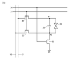
도 3은 화소의 일례를 도시한 도면.
도 4는 화소의 동작의 일례를 도시한 도면.
도 5는 화소의 일례를 도시한 도면.
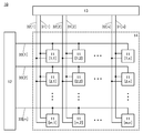
도 6은 표시 장치의 일례를 도시한 도면.
도 7은 소스 드라이버 회로의 일례를 도시한 도면 및 패스 트랜지스터 로직 회로의 특성의 일례를 도시한 도면.
도 8은 소스 드라이버 회로의 일례를 도시한 도면 및 패스 트랜지스터 로직 회로의 특성의 일례를 도시한 도면.
도 9는 표시 장치의 일례를 도시한 도면.
도 10은 트랜지스터의 일례를 도시한 도면.
도 11은 트랜지스터의 일례를 도시한 도면.
도 12는 트랜지스터의 일례를 도시한 도면.
도 13은 트랜지스터의 일례를 도시한 도면.
도 14는 전자 기기의 일례를 도시한 도면.
도 15는 실시예 1에서 사용한 회로를 도시한 도면.
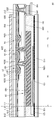
도 16은 실시예 1에서 사용한 화소를 도시한 도면.
도 17은 실시예 1에서의 계산 조건을 나타낸 도면.
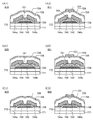
도 18은 실시예 1에서의 계산 결과를 나타낸 도면.
Claims (13)
- 화소 및 소스 드라이버 회로를 가지는 표시 장치로서,
상기 화소는 제 1 트랜지스터, 제 2 트랜지스터, 용량 소자, 및 표시 디바이스를 가지고,
상기 제 1 트랜지스터의 소스 및 드레인 중 한쪽은 상기 용량 소자의 한쪽 전극에 전기적으로 접속되고,
상기 용량 소자의 한쪽 전극은 상기 표시 디바이스의 한쪽 전극에 전기적으로 접속되고,
상기 제 2 트랜지스터의 소스 및 드레인 중 한쪽은 상기 용량 소자의 다른 쪽 전극에 전기적으로 접속되고,
상기 용량 소자의 다른 쪽 전극은 상기 표시 디바이스의 다른 쪽 전극에 전기적으로 접속되고,
상기 제 1 트랜지스터의 소스 및 드레인 중 다른 쪽은 제 1 배선을 통하여 상기 소스 드라이버 회로에 전기적으로 접속되고,
상기 제 2 트랜지스터의 소스 및 드레인 중 다른 쪽은 제 2 배선을 통하여 상기 소스 드라이버 회로에 전기적으로 접속되는, 표시 장치. - 제 1 항에 있어서,
상기 소스 드라이버 회로는 상기 제 2 배선에 제 1 전위 또는 제 2 전위를 공급하는 기능을 가지고,
상기 소스 드라이버 회로는 제 1 저항 소자 및 제 2 저항 소자를 가지고,
상기 제 1 저항 소자의 한쪽 단자에는 상기 제 1 전위가 공급되고,
상기 제 2 저항 소자의 한쪽 단자에는 상기 제 2 전위가 공급되는, 표시 장치. - 제 2 항에 있어서,
상기 소스 드라이버 회로는 제 1 스위치 및 제 2 스위치를 가지고,
상기 제 1 저항 소자의 한쪽 단자는 상기 제 1 스위치의 한쪽 단자에 전기적으로 접속되고,
상기 제 1 스위치의 다른 쪽 단자는 상기 제 2 배선에 전기적으로 접속되고,
상기 제 2 저항 소자의 한쪽 단자는 상기 제 2 스위치의 한쪽 단자에 전기적으로 접속되고,
상기 제 2 스위치의 다른 쪽 단자는 상기 제 2 배선에 전기적으로 접속되는, 표시 장치. - 제 2 항 또는 제 3 항에 있어서,
상기 제 1 전위는 양의 전위이고,
상기 제 2 전위는 음의 전위인, 표시 장치. - 제 4 항에 있어서,
상기 제 1 전위의 절댓값과 상기 제 2 전위의 절댓값은 동일 또는 대략 동일한, 표시 장치. - 제 1 항 내지 제 5 항 중 어느 한 항에 있어서,
상기 제 1 트랜지스터의 게이트 및 상기 제 2 트랜지스터의 게이트는 제 3 배선에 전기적으로 접속되는, 표시 장치. - 제 1 항 내지 제 6 항 중 어느 한 항에 있어서,
상기 표시 장치는 게이트 드라이버 회로를 가지고,
상기 제 3 배선은 상기 게이트 드라이버 회로에 전기적으로 접속되는, 표시 장치. - 제 1 항 내지 제 7 항 중 어느 한 항에 있어서,
상기 표시 디바이스는 액정 디바이스인, 표시 장치. - 제 8 항에 있어서,
상기 표시 디바이스는 수평 전계 방식이 적용된 액정 디바이스인, 표시 장치. - 제 9 항에 있어서,
상기 표시 디바이스는 블루상을 나타내는 액정을 가지는, 표시 장치. - 제 1 항 내지 제 10 항 중 어느 한 항에 있어서,
상기 제 1 트랜지스터 및 상기 제 2 트랜지스터는 채널 형성 영역에 금속 산화물을 가지고,
상기 금속 산화물은 In, Zn, 및 M(M은 Al, Ti, Ga, Sn, Y, Zr, La, Ce, Nd, 또는 Hf)을 가지는, 표시 장치. - 제 1 항 내지 제 11 항 중 어느 한 항에 있어서,
상기 화소는 제 3 트랜지스터를 가지고,
상기 제 3 트랜지스터의 소스 및 드레인 중 한쪽은 상기 표시 디바이스의 다른 쪽 전극에 전기적으로 접속되고,
상기 제 3 트랜지스터의 소스 및 드레인 중 한쪽은 공통 배선에 전기적으로 접속되는, 표시 장치. - 제 12 항에 있어서,
상기 제 3 트랜지스터는 채널 형성 영역에 금속 산화물을 가지고,
상기 금속 산화물은 In, Zn, 및 M(M은 Al, Ti, Ga, Sn, Y, Zr, La, Ce, Nd, 또는 Hf)을 가지는, 표시 장치.
Applications Claiming Priority (3)
| Application Number | Priority Date | Filing Date | Title |
|---|---|---|---|
| JPJP-P-2017-245734 | 2017-12-22 | ||
| JP2017245734 | 2017-12-22 | ||
| PCT/IB2018/059983 WO2019123130A1 (ja) | 2017-12-22 | 2018-12-13 | 表示装置 |
Publications (2)
| Publication Number | Publication Date |
|---|---|
| KR20200093650A true KR20200093650A (ko) | 2020-08-05 |
| KR102599913B1 KR102599913B1 (ko) | 2023-11-07 |
Family
ID=66994526
Family Applications (1)
| Application Number | Title | Priority Date | Filing Date |
|---|---|---|---|
| KR1020207019643A Active KR102599913B1 (ko) | 2017-12-22 | 2018-12-13 | 표시 장치 |
Country Status (6)
| Country | Link |
|---|---|
| US (1) | US11217190B2 (ko) |
| EP (1) | EP3731008A4 (ko) |
| JP (1) | JP7321942B2 (ko) |
| KR (1) | KR102599913B1 (ko) |
| CN (2) | CN117008384A (ko) |
| WO (1) | WO2019123130A1 (ko) |
Families Citing this family (3)
| Publication number | Priority date | Publication date | Assignee | Title |
|---|---|---|---|---|
| JP7291631B2 (ja) | 2017-12-21 | 2023-06-15 | 株式会社半導体エネルギー研究所 | 表示装置 |
| CN115208167A (zh) * | 2022-07-08 | 2022-10-18 | 武汉华星光电技术有限公司 | 半导体器件和电子终端 |
| JP2025104949A (ja) * | 2023-12-28 | 2025-07-10 | エルジー ディスプレイ カンパニー リミテッド | 空間光変調装置 |
Citations (6)
| Publication number | Priority date | Publication date | Assignee | Title |
|---|---|---|---|---|
| JPH11119193A (ja) | 1997-10-16 | 1999-04-30 | Sony Corp | 液晶表示装置 |
| JP2005258417A (ja) * | 2004-02-09 | 2005-09-22 | Advanced Lcd Technologies Development Center Co Ltd | 液晶画素メモリ、液晶表示装置およびこれらの駆動方法 |
| KR20080013736A (ko) * | 2006-08-07 | 2008-02-13 | 세이코 엡슨 가부시키가이샤 | 전기 광학 소자의 구동 방법, 화소 회로, 전기 광학 장치및 전자 기기 |
| KR20090077707A (ko) * | 2008-01-11 | 2009-07-15 | 도시바 모바일 디스플레이 가부시키가이샤 | 액정 표시 장치 |
| KR20100063660A (ko) * | 2008-12-03 | 2010-06-11 | 가부시키가이샤 한도오따이 에네루기 켄큐쇼 | 액정 표시 장치 |
| KR20100100243A (ko) * | 2009-03-05 | 2010-09-15 | 삼성전자주식회사 | 액정 표시 장치 및 액정 표시 장치의 구동 방법 |
Family Cites Families (20)
| Publication number | Priority date | Publication date | Assignee | Title |
|---|---|---|---|---|
| DE69428363T2 (de) | 1994-06-24 | 2002-04-18 | Hitachi Ltd | Flüssigkristallanzeigevorrichtung mit aktiver matrix und steuerverfahren dafür |
| US6198464B1 (en) | 1995-01-13 | 2001-03-06 | Hitachi, Ltd. | Active matrix type liquid crystal display system and driving method therefor |
| DE10303427A1 (de) | 2002-02-06 | 2003-10-16 | Nec Corp Tokio Tokyo | Verstärker-Schaltung, Treiber-Schaltung für ein Anzeigegerät , tragbares Telefon und tragbares elektronisches Gerät |
| JP4487488B2 (ja) * | 2002-03-13 | 2010-06-23 | 日本電気株式会社 | 表示装置の駆動回路、携帯電話機及び携帯用電子機器 |
| JP2003302942A (ja) | 2002-04-09 | 2003-10-24 | Hitachi Displays Ltd | 画像表示装置 |
| US7425940B2 (en) | 2004-02-09 | 2008-09-16 | Advanced Lcd Technologies Development Center Co., Ltd. | Liquid crystal pixel memory, liquid crystal display, and methods of driving the same |
| CN100414596C (zh) * | 2005-12-02 | 2008-08-27 | 群康科技(深圳)有限公司 | 液晶显示器及其驱动电路与驱动方法 |
| KR101245944B1 (ko) * | 2006-05-10 | 2013-03-21 | 엘지디스플레이 주식회사 | 액정패널, 이를 구비한 액정표시장치 및 그 구동 방법 |
| JP2008250118A (ja) * | 2007-03-30 | 2008-10-16 | Seiko Epson Corp | 液晶装置、液晶装置の駆動回路、液晶装置の駆動方法および電子機器 |
| CN100483241C (zh) * | 2007-06-28 | 2009-04-29 | 友达光电股份有限公司 | 液晶显示装置、栅极驱动电路及其驱动电路单元 |
| JP5093730B2 (ja) * | 2007-07-09 | 2012-12-12 | Nltテクノロジー株式会社 | 液晶表示装置 |
| KR101046929B1 (ko) | 2008-06-16 | 2011-07-06 | 삼성전자주식회사 | 액정 표시 장치 |
| US8760479B2 (en) | 2008-06-16 | 2014-06-24 | Samsung Display Co., Ltd. | Liquid crystal display |
| JP2011107692A (ja) * | 2009-10-20 | 2011-06-02 | Semiconductor Energy Lab Co Ltd | 表示装置の駆動方法、表示装置、及び電子機器。 |
| US8373621B2 (en) * | 2009-12-01 | 2013-02-12 | Samsung Display Co., Ltd. | Array substrate and liquid crystal display device having the same |
| US20110279427A1 (en) | 2010-05-14 | 2011-11-17 | Semiconductor Energy Laboratory Co., Ltd. | Liquid crystal display device and electronic appliance |
| JP5775357B2 (ja) | 2010-05-21 | 2015-09-09 | 株式会社半導体エネルギー研究所 | 液晶表示装置 |
| JP6698321B2 (ja) | 2014-12-02 | 2020-05-27 | 株式会社半導体エネルギー研究所 | 表示装置 |
| US10140940B2 (en) | 2015-07-24 | 2018-11-27 | Japan Display Inc. | Display device |
| US10007161B2 (en) * | 2015-10-26 | 2018-06-26 | Semiconductor Energy Laboratory Co., Ltd. | Display device |
-
2018
- 2018-12-13 JP JP2019560507A patent/JP7321942B2/ja active Active
- 2018-12-13 CN CN202310769449.3A patent/CN117008384A/zh active Pending
- 2018-12-13 CN CN201880077376.9A patent/CN111417895B/zh active Active
- 2018-12-13 KR KR1020207019643A patent/KR102599913B1/ko active Active
- 2018-12-13 US US16/770,998 patent/US11217190B2/en not_active Expired - Fee Related
- 2018-12-13 WO PCT/IB2018/059983 patent/WO2019123130A1/ja not_active Ceased
- 2018-12-13 EP EP18890303.3A patent/EP3731008A4/en not_active Withdrawn
Patent Citations (6)
| Publication number | Priority date | Publication date | Assignee | Title |
|---|---|---|---|---|
| JPH11119193A (ja) | 1997-10-16 | 1999-04-30 | Sony Corp | 液晶表示装置 |
| JP2005258417A (ja) * | 2004-02-09 | 2005-09-22 | Advanced Lcd Technologies Development Center Co Ltd | 液晶画素メモリ、液晶表示装置およびこれらの駆動方法 |
| KR20080013736A (ko) * | 2006-08-07 | 2008-02-13 | 세이코 엡슨 가부시키가이샤 | 전기 광학 소자의 구동 방법, 화소 회로, 전기 광학 장치및 전자 기기 |
| KR20090077707A (ko) * | 2008-01-11 | 2009-07-15 | 도시바 모바일 디스플레이 가부시키가이샤 | 액정 표시 장치 |
| KR20100063660A (ko) * | 2008-12-03 | 2010-06-11 | 가부시키가이샤 한도오따이 에네루기 켄큐쇼 | 액정 표시 장치 |
| KR20100100243A (ko) * | 2009-03-05 | 2010-09-15 | 삼성전자주식회사 | 액정 표시 장치 및 액정 표시 장치의 구동 방법 |
Also Published As
| Publication number | Publication date |
|---|---|
| CN111417895B (zh) | 2023-06-16 |
| CN111417895A (zh) | 2020-07-14 |
| JPWO2019123130A1 (ja) | 2021-01-14 |
| WO2019123130A1 (ja) | 2019-06-27 |
| CN117008384A (zh) | 2023-11-07 |
| KR102599913B1 (ko) | 2023-11-07 |
| EP3731008A1 (en) | 2020-10-28 |
| EP3731008A4 (en) | 2021-07-21 |
| US20200372868A1 (en) | 2020-11-26 |
| US11217190B2 (en) | 2022-01-04 |
| JP7321942B2 (ja) | 2023-08-07 |
Similar Documents
| Publication | Publication Date | Title |
|---|---|---|
| JP7410110B2 (ja) | 半導体装置 | |
| CN111406280B (zh) | 半导体装置、显示装置、电子设备及工作方法 | |
| KR102403389B1 (ko) | 표시 장치 및 전자 기기 | |
| JP2023171396A (ja) | 半導体装置 | |
| CN110651358A (zh) | 半导体装置、显示装置以及半导体装置的制造方法 | |
| KR102915517B1 (ko) | 반도체 장치의 제작 방법 | |
| WO2017115222A1 (en) | Metal oxide film and semiconductor device | |
| KR102567675B1 (ko) | 화상 처리 방법 | |
| JP2024037777A (ja) | 半導体装置の作製方法 | |
| US12353105B2 (en) | Display apparatus | |
| KR102599913B1 (ko) | 표시 장치 | |
| JP2023111947A (ja) | 表示装置の動作方法 | |
| JP6983597B2 (ja) | 表示装置および電子機器 | |
| TW201727910A (zh) | 氧化物半導體膜,半導體裝置,及顯示裝置 | |
| JP7289793B2 (ja) | 表示装置およびその補正方法 | |
| JP7374886B2 (ja) | 表示装置 |
Legal Events
| Date | Code | Title | Description |
|---|---|---|---|
| PA0105 | International application |
Patent event date: 20200707 Patent event code: PA01051R01D Comment text: International Patent Application |
|
| PG1501 | Laying open of application | ||
| A201 | Request for examination | ||
| PA0201 | Request for examination |
Patent event code: PA02012R01D Patent event date: 20211118 Comment text: Request for Examination of Application |
|
| E902 | Notification of reason for refusal | ||
| PE0902 | Notice of grounds for rejection |
Comment text: Notification of reason for refusal Patent event date: 20230224 Patent event code: PE09021S01D |
|
| E701 | Decision to grant or registration of patent right | ||
| PE0701 | Decision of registration |
Patent event code: PE07011S01D Comment text: Decision to Grant Registration Patent event date: 20230829 |
|
| GRNT | Written decision to grant | ||
| PR0701 | Registration of establishment |
Comment text: Registration of Establishment Patent event date: 20231103 Patent event code: PR07011E01D |
|
| PR1002 | Payment of registration fee |
Payment date: 20231103 End annual number: 3 Start annual number: 1 |
|
| PG1601 | Publication of registration |