KR20210117536A - An electronic device including a plurality of antennas - Google Patents

An electronic device including a plurality of antennas Download PDF

Info

Publication number
KR20210117536A
KR20210117536A KR1020200033851A KR20200033851A KR20210117536A KR 20210117536 A KR20210117536 A KR 20210117536A KR 1020200033851 A KR1020200033851 A KR 1020200033851A KR 20200033851 A KR20200033851 A KR 20200033851A KR 20210117536 A KR20210117536 A KR 20210117536A
Authority
KR
South Korea
Prior art keywords
antenna
conductive pattern
disposed
frequency band
dielectric substrate
Prior art date
Legal status (The legal status is an assumption and is not a legal conclusion. Google has not performed a legal analysis and makes no representation as to the accuracy of the status listed.)
Granted
Application number
KR1020200033851A
Other languages
Korean (ko)
Other versions
KR102732974B1 (en
Inventor
박우진
최동욱
서정훈
이종인
최휘경
Original Assignee
삼성전자주식회사
Priority date (The priority date is an assumption and is not a legal conclusion. Google has not performed a legal analysis and makes no representation as to the accuracy of the date listed.)
Filing date
Publication date
Application filed by 삼성전자주식회사 filed Critical 삼성전자주식회사
Priority to KR1020200033851A priority Critical patent/KR102732974B1/en
Priority to EP21771921.0A priority patent/EP4123831A4/en
Priority to PCT/KR2021/002947 priority patent/WO2021187794A1/en
Publication of KR20210117536A publication Critical patent/KR20210117536A/en
Priority to US17/943,679 priority patent/US12100899B2/en
Application granted granted Critical
Publication of KR102732974B1 publication Critical patent/KR102732974B1/en
Active legal-status Critical Current
Anticipated expiration legal-status Critical

Links

Images

Classifications

    • HELECTRICITY
    • H01ELECTRIC ELEMENTS
    • H01QANTENNAS, i.e. RADIO AERIALS
    • H01Q1/00Details of, or arrangements associated with, antennas
    • H01Q1/36Structural form of radiating elements, e.g. cone, spiral, umbrella; Particular materials used therewith
    • H01Q1/38Structural form of radiating elements, e.g. cone, spiral, umbrella; Particular materials used therewith formed by a conductive layer on an insulating support
    • HELECTRICITY
    • H01ELECTRIC ELEMENTS
    • H01QANTENNAS, i.e. RADIO AERIALS
    • H01Q21/00Antenna arrays or systems
    • H01Q21/06Arrays of individually energised antenna units similarly polarised and spaced apart
    • H01Q21/20Arrays of individually energised antenna units similarly polarised and spaced apart the units being spaced along or adjacent to a curvilinear path
    • H01Q21/205Arrays of individually energised antenna units similarly polarised and spaced apart the units being spaced along or adjacent to a curvilinear path providing an omnidirectional coverage
    • HELECTRICITY
    • H01ELECTRIC ELEMENTS
    • H01QANTENNAS, i.e. RADIO AERIALS
    • H01Q1/00Details of, or arrangements associated with, antennas
    • H01Q1/12Supports; Mounting means
    • H01Q1/22Supports; Mounting means by structural association with other equipment or articles
    • H01Q1/2291Supports; Mounting means by structural association with other equipment or articles used in Bluetooth® or Wi-Fi® devices of Wireless Local Area Networks [WLAN]
    • HELECTRICITY
    • H01ELECTRIC ELEMENTS
    • H01QANTENNAS, i.e. RADIO AERIALS
    • H01Q1/00Details of, or arrangements associated with, antennas
    • H01Q1/12Supports; Mounting means
    • H01Q1/22Supports; Mounting means by structural association with other equipment or articles
    • H01Q1/24Supports; Mounting means by structural association with other equipment or articles with receiving set
    • H01Q1/241Supports; Mounting means by structural association with other equipment or articles with receiving set used in mobile communications, e.g. GSM
    • H01Q1/242Supports; Mounting means by structural association with other equipment or articles with receiving set used in mobile communications, e.g. GSM specially adapted for hand-held use
    • H01Q1/243Supports; Mounting means by structural association with other equipment or articles with receiving set used in mobile communications, e.g. GSM specially adapted for hand-held use with built-in antennas
    • HELECTRICITY
    • H01ELECTRIC ELEMENTS
    • H01QANTENNAS, i.e. RADIO AERIALS
    • H01Q21/00Antenna arrays or systems
    • H01Q21/24Combinations of antenna units polarised in different directions for transmitting or receiving circularly and elliptically polarised waves or waves linearly polarised in any direction
    • HELECTRICITY
    • H01ELECTRIC ELEMENTS
    • H01QANTENNAS, i.e. RADIO AERIALS
    • H01Q21/00Antenna arrays or systems
    • H01Q21/28Combinations of substantially independent non-interacting antenna units or systems
    • HELECTRICITY
    • H01ELECTRIC ELEMENTS
    • H01QANTENNAS, i.e. RADIO AERIALS
    • H01Q5/00Arrangements for simultaneous operation of antennas on two or more different wavebands, e.g. dual-band or multi-band arrangements
    • H01Q5/30Arrangements for providing operation on different wavebands
    • H01Q5/307Individual or coupled radiating elements, each element being fed in an unspecified way
    • H01Q5/342Individual or coupled radiating elements, each element being fed in an unspecified way for different propagation modes
    • H01Q5/357Individual or coupled radiating elements, each element being fed in an unspecified way for different propagation modes using a single feed point
    • HELECTRICITY
    • H01ELECTRIC ELEMENTS
    • H01QANTENNAS, i.e. RADIO AERIALS
    • H01Q9/00Electrically-short antennas having dimensions not more than twice the operating wavelength and consisting of conductive active radiating elements
    • H01Q9/04Resonant antennas
    • H01Q9/06Details
    • H01Q9/065Microstrip dipole antennas
    • HELECTRICITY
    • H04ELECTRIC COMMUNICATION TECHNIQUE
    • H04BTRANSMISSION
    • H04B7/00Radio transmission systems, i.e. using radiation field
    • H04B7/02Diversity systems; Multi-antenna system, i.e. transmission or reception using multiple antennas
    • H04B7/04Diversity systems; Multi-antenna system, i.e. transmission or reception using multiple antennas using two or more spaced independent antennas
    • H04B7/0413MIMO systems

Landscapes

  • Engineering & Computer Science (AREA)
  • Computer Networks & Wireless Communication (AREA)
  • Signal Processing (AREA)
  • Support Of Aerials (AREA)
  • Transceivers (AREA)
  • Telephone Set Structure (AREA)
  • Details Of Aerials (AREA)

Abstract

본 개시는 복수의 안테나를 포함하는 전자 장치에 관한 것으로, 본 개시의 일 실시예에 따른 전자 장치는, 하우징, 상기 하우징 내에 배치되는 제1 안테나, 상기 하우징 내에 배치되고, 상기 제1 안테나와 이격되어 배치되는 제2 안테나, 상기 하우징 내에 배치되는 인쇄 회로 기판 및 상기 인쇄 회로 기판에 배치되고, 상기 제1 안테나와 상기 제2 안테나를 통해 지정된 주파수 대역의 RF 신호를 송신 또는 수신하는 무선 통신 회로를 포함하고, 상기 제1 안테나는, 제1 면과 상기 제1 면과 반대 방향을 향하는 제2 면을 포함하는 제1 유전체 기판, 상기 제1 면에 배치되고, 제1 주파수 대역의 RF 신호를 송신 또는 수신하는 안테나 방사체로 동작하는 제1 도전성 패턴 및 상기 제2 면에 배치되고, 제1 주파수 대역의 RF 신호를 송신 또는 수신하는 안테나 방사체로 동작하는 제2 도전성 패턴을 포함하고, 상기 제2 안테나는, 제3 면과 상기 제3 면과 반대 방향을 향하는 제4 면을 포함하는 제2 유전체 기판, 상기 제3 면에 배치되고, 제1 주파수 대역의 RF 신호를 송신 또는 수신하는 안테나 방사체로 동작하는 제3 도전성 패턴 및 상기 제4 면에 배치되고, 제1 주파수 대역의 RF 신호를 송신 또는 수신하는 안테나 방사체로 동작하는 제4 도전성 패턴을 포함하고, 상기 제1 안테나의 상기 제1 면 상에서 봤을 때, 상기 제1 도전성 패턴과 상기 제2 도전성 패턴은 서로 수직을 이루고, 상기 제2 안테나의 상기 제4 면 상에서 봤을 때, 상기 제3 도전성 패턴과 상기 제4 도전성 패턴은 서로 수직을 이루며, 상기 제1 안테나의 상기 제2 면과 상기 제2 안테나의 제3 면은 서로 마주보도록 배치될 수 있다.The present disclosure relates to an electronic device including a plurality of antennas, and an electronic device according to an embodiment of the present disclosure includes a housing, a first antenna disposed in the housing, disposed in the housing, and spaced apart from the first antenna a second antenna disposed as being disposed, a printed circuit board disposed in the housing, and a wireless communication circuit disposed on the printed circuit board and transmitting or receiving an RF signal of a specified frequency band through the first antenna and the second antenna; a first dielectric substrate including a first surface and a second surface facing in a direction opposite to the first surface, the first antenna being disposed on the first surface, and transmitting an RF signal of a first frequency band or a first conductive pattern serving as an antenna radiator for receiving and a second conductive pattern disposed on the second surface and operating as an antenna radiator for transmitting or receiving an RF signal of a first frequency band, the second antenna is a second dielectric substrate including a third surface and a fourth surface facing in a direction opposite to the third surface, and is disposed on the third surface and operates as an antenna radiator for transmitting or receiving an RF signal of a first frequency band and a third conductive pattern disposed on the fourth surface, and a fourth conductive pattern operating as an antenna radiator for transmitting or receiving an RF signal of a first frequency band, wherein when viewed from the first surface of the first antenna when the first conductive pattern and the second conductive pattern are perpendicular to each other, when viewed from the fourth surface of the second antenna, the third conductive pattern and the fourth conductive pattern are perpendicular to each other, The second surface of the first antenna and the third surface of the second antenna may be disposed to face each other.

Description

복수의 안테나를 포함하는 전자 장치{AN ELECTRONIC DEVICE INCLUDING A PLURALITY OF ANTENNAS}Electronic device including a plurality of antennas

본 개시의 다양한 실시예들은 복수의 안테나를 포함하는 전자 장치에 관한 것이다.Various embodiments of the present disclosure relate to an electronic device including a plurality of antennas.

액세스 포인트(AP: access point)(또는 무선 접속 장치)는 무선 장치들을 네트워크에 연결할 수 있도록 도와주는 전자 장치를 의미한다. 사용자들은 액세스 포인트를 통해 특정 서비스 제공 지역 내에서 모바일 전자 장치, 컴퓨터, 또는 휴대용 멀티미디어 기기와 같은 전자 장치를 네트워크에 연결할 수 있으며, 네트워크에 연결된 전자 장치는 무선 주파수를 통해 데이터를 송신 또는 수신할 수 있다.An access point (AP) (or wireless access device) refers to an electronic device that helps wireless devices connect to a network. The access point allows users to connect electronic devices such as mobile electronic devices, computers, or portable multimedia devices to the network within a specific service area, and the electronic devices connected to the network can transmit or receive data via radio frequencies. have.

무선 통신 기술을 사용하여 네트워크에 연결하는 전자 장치가 증가함에 따라, 무선 주파수를 통해 송신 또는 수신되는 데이터의 용량이 급격하게 증가하게 되었다. 데이터 용량의 증가함에 따라, 최근의 액세스 포인트에는 송신 또는 수신되는 데이터 용량을 높일 수 있는 다중 입출력(MIMO: multiple input and multiple output) 기술이 적용될 수 있다.As the number of electronic devices connecting to a network using a wireless communication technology increases, the capacity of data transmitted or received through a radio frequency has rapidly increased. As the data capacity increases, a multiple input and multiple output (MIMO) technology capable of increasing the data capacity to be transmitted or received may be applied to recent access points.

다중 입출력(MIMO) 기술을 구현하기 위해서는 전자 장치(예: 액세스 포인트) 내에 복수의 안테나가 배치되어야 한다. 예를 들어, 4x4 다중 입출력(MIMO) 기술의 구현을 위해서는 액세스 포인트 내에 4개의 안테나가 배치되어야 하며, 8x8 다중 입출력(MIMO) 기술의 구현을 위해서는 전자 장치 내에 8개의 안테나가 배치되어야 한다.In order to implement multiple input/output (MIMO) technology, a plurality of antennas must be disposed within an electronic device (eg, an access point). For example, in order to implement a 4x4 multiple input/output (MIMO) technology, four antennas should be arranged in an access point, and to implement an 8x8 multiple input/output (MIMO) technology, eight antennas should be arranged in an electronic device.

전자 장치는, 무선 주파수를 통한 데이터 송신 또는 수신되는 IEEE(institute of electrical and electronics engineers)에서 정의된 표준을 지원할 수 있다. IEEE 802.11ax(또는 "WiFi 6") 표준에 의하면, 전자 장치는 2.4 GHz, 5 GHz 로우 밴드(LB), 및/또는 5 GHz 하이 밴드(HB)의 3개의 주파수 대역(tri band)을 지원할 수 있다. The electronic device may support a standard defined by an Institute of Electrical and Electronics Engineers (IEEE) in which data is transmitted or received through a radio frequency. According to the IEEE 802.11ax (or "WiFi 6") standard, an electronic device can support three frequency bands (tri bands): 2.4 GHz, 5 GHz low band (LB), and/or 5 GHz high band (HB). have.

다중 입출력(MIMO) 기술을 구현하면서, IEEE 802.11ax 표준에서 지원하는 주파수 대역까지 지원하기 위해서는, 전자 장치 내에 배치되어야 하는 안테나의 개수가 급수적으로 증가할 수 있다. 일 예시에서, 전자 장치 내에 배치되어야 하는 안테나의 개수가 증가할수록 전자 장치의 부피가 증가할 수 있다. 다른 예시에서, 전자 장치 내에 배치되어야 하는 안테나의 개수가 증가할수록 안테나가 배치될 수 있는 공간이 줄어들어, 전자 장치 내에 복수의 안테나가 인접하게 배치될 수 있으며, 이에 따라 안테나 사이의 간섭이 발생하여 액세스 포인트의 성능(예: 방사 성능) 열화가 발생할 수 있다.In order to support up to a frequency band supported by the IEEE 802.11ax standard while implementing the multiple input/output (MIMO) technology, the number of antennas to be disposed in the electronic device may increase exponentially. In one example, as the number of antennas to be disposed in the electronic device increases, the volume of the electronic device may increase. In another example, as the number of antennas to be disposed in the electronic device increases, the space in which the antennas can be disposed decreases, so that a plurality of antennas may be disposed adjacently in the electronic device, thereby causing interference between the antennas to access Degradation of the point's performance (eg radiant performance) may occur.

본 개시의 다양한 실시예들은 안테나 개수를 줄이면서, 다중 입출력(MIMO) 기술 및 IEEE 표준을 지원할 수 있는 전자 장치(또는 액세스 포인트)를 제공하고자 한다.Various embodiments of the present disclosure provide an electronic device (or access point) capable of supporting multiple input/output (MIMO) technology and IEEE standards while reducing the number of antennas.

본 개시의 일 실시예에 따른 전자 장치는, 하우징, 상기 하우징 내에 배치되는 제1 안테나, 상기 하우징 내에 배치되고, 상기 제1 안테나와 이격되어 배치되는 제2 안테나, 상기 하우징 내에 배치되는 인쇄 회로 기판 및 상기 인쇄 회로 기판에 배치되고, 상기 제1 안테나와 상기 제2 안테나를 통해 지정된 주파수 대역의 RF 신호를 송신 또는 수신하는 무선 통신 회로를 포함하고, 상기 제1 안테나는, 제1 면과 상기 제1 면과 반대 방향을 향하는 제2 면을 포함하는 제1 유전체 기판, 상기 제1 면에 배치되고, 제1 주파수 대역의 RF 신호를 송신 또는 수신하는 안테나 방사체로 동작하는 제1 도전성 패턴 및 상기 제2 면에 배치되고, 제1 주파수 대역의 RF 신호를 송신 또는 수신하는 안테나 방사체로 동작하는 제2 도전성 패턴을 포함하고, 상기 제2 안테나는, 제3 면과 상기 제3 면과 반대 방향을 향하는 제4 면을 포함하는 제2 유전체 기판, 상기 제3 면에 배치되고, 제1 주파수 대역의 RF 신호를 송신 또는 수신하는 안테나 방사체로 동작하는 제3 도전성 패턴 및 상기 제4 면에 배치되고, 제1 주파수 대역의 RF 신호를 송신 또는 수신하는 안테나 방사체로 동작하는 제4 도전성 패턴을 포함하고, 상기 제1 안테나의 상기 제1 면 상에서 봤을 때, 상기 제1 도전성 패턴과 상기 제2 도전성 패턴은 서로 수직을 이루고, 상기 제2 안테나의 상기 제4 면 상에서 봤을 때, 상기 제3 도전성 패턴과 상기 제4 도전성 패턴은 서로 수직을 이루며, 상기 제1 안테나의 상기 제2 면과 상기 제2 안테나의 제3 면은 서로 마주보도록 배치될 수 있다.An electronic device according to an embodiment of the present disclosure includes a housing, a first antenna disposed in the housing, a second antenna disposed in the housing and spaced apart from the first antenna, and a printed circuit board disposed in the housing. and a wireless communication circuit disposed on the printed circuit board and configured to transmit or receive an RF signal of a specified frequency band through the first antenna and the second antenna, wherein the first antenna includes a first surface and the second antenna A first dielectric substrate including a second surface facing in a direction opposite to the first surface, a first conductive pattern disposed on the first surface and operating as an antenna radiator for transmitting or receiving an RF signal of a first frequency band; and a second conductive pattern disposed on two surfaces and operating as an antenna radiator for transmitting or receiving an RF signal of a first frequency band, wherein the second antenna has a third surface and a direction opposite to the third surface A second dielectric substrate including a fourth surface, a third conductive pattern disposed on the third surface and operating as an antenna radiator for transmitting or receiving an RF signal of a first frequency band, and disposed on the fourth surface, and a fourth conductive pattern operating as an antenna radiator for transmitting or receiving an RF signal of a first frequency band, wherein when viewed from the first surface of the first antenna, the first conductive pattern and the second conductive pattern are mutually is perpendicular, and when viewed from the fourth surface of the second antenna, the third conductive pattern and the fourth conductive pattern are perpendicular to each other, and the second surface of the first antenna and the second surface of the second antenna The three surfaces may be disposed to face each other.

본 개시의 다른 실시예에 따른 전자 장치는, 하우징, 상기 하우징 내에 배치되는 제1 안테나, 상기 하우징 내에 배치되고, 상기 제1 안테나와 이격되어 배치되는 제2 안테나, 상기 하우징 내에 배치되는 인쇄 회로 기판 및 상기 인쇄 회로 기판에 배치되고, 상기 제1 안테나와 상기 제2 안테나를 통해 지정된 주파수 대역의 RF 신호를 송신 또는 수신하는 무선 통신 회로를 포함하고, 상기 제1 안테나는, 제1 유전체 기판, 상기 제1 유전체 기판의 일면에 배치되고, 제1 주파수 대역의 RF 신호를 송신 또는 수신하는 안테나 방사체로 동작하는 제1 도전성 패턴 및 상기 제1 유전체 기판의 상기 일면과 반대 방향을 향하는 다른 일면에 배치되고, 제2 주파수 대역의 RF 신호를 송신 또는 수신하는 안테나 방사체로 동작하는 제2 도전성 패턴을 포함하고, 상기 제2 안테나는, 제2 유전체 기판, 상기 제2 유전체 기판의 일면에 배치되고, 상기 제1 주파수 대역의 RF 신호를 송신 또는 수신하는 안테나 방사체로 동작하는 제3 도전성 패턴 및 상기 제2 유전체 기판의 상기 일면과 반대 방향을 향하는 다른 일면에 배치되고, 상기 제2 주파수 대역의 RF 신호를 송신 또는 수신하는 안테나 방사체로 동작하는 제4 도전성 패턴을 포함하고, 상기 제1 유전체 기판의 적어도 일면은 상기 제2 유전체 기판의 적어도 일면을 마주보도록 배치될 수 있다.An electronic device according to another embodiment of the present disclosure includes a housing, a first antenna disposed in the housing, a second antenna disposed in the housing and spaced apart from the first antenna, and a printed circuit board disposed in the housing. and a wireless communication circuit disposed on the printed circuit board and configured to transmit or receive an RF signal of a specified frequency band through the first antenna and the second antenna, wherein the first antenna comprises: a first dielectric substrate; A first conductive pattern disposed on one surface of the first dielectric substrate and operating as an antenna radiator for transmitting or receiving an RF signal of a first frequency band and disposed on the other surface of the first dielectric substrate facing in a direction opposite to the one surface, , a second conductive pattern operating as an antenna radiator for transmitting or receiving an RF signal of a second frequency band, wherein the second antenna is disposed on a second dielectric substrate and one surface of the second dielectric substrate, A third conductive pattern serving as an antenna radiator for transmitting or receiving an RF signal of one frequency band and disposed on the other surface of the second dielectric substrate facing the opposite direction to the one surface, transmitting the RF signal of the second frequency band Alternatively, a fourth conductive pattern serving as a receiving antenna radiator may be included, and at least one surface of the first dielectric substrate may be disposed to face at least one surface of the second dielectric substrate.

본 개시의 또 다른 실시예에 따른 전자 장치는, 하우징, 상기 하우징 내에 배치되는 제1 안테나, 상기 하우징 내에 배치되고, 상기 제1 안테나와 이격되어 배치되는 제2 안테나, 상기 하우징 내에 배치되고, 상기 제1 안테나 및 상기 제2 안테나와 이격되어 배치되는 제3 안테나, 상기 하우징 내에 배치되고, 상기 제3 안테나와 마주보도록 배치되는 제4 안테나, 상기 하우징 내에 배치되는 인쇄 회로 기판 및 상기 인쇄 회로 기판에 배치되고, 상기 제1 안테나, 상기 제2 안테나 및 상기 제3 안테나를 통하여 지정된 주파수 대역의 RF 신호를 송신 또는 수신하는 무선 통신 회로를 포함하고, 상기 제1 안테나는, 제1 면과 상기 제1 면과 반대 방향을 향하는 제2 면을 포함하는 제1 유전체 기판, 상기 제1 면에 배치되고, 제1 주파수 대역의 RF 신호를 송신 또는 수신하는 안테나 방사체로 동작하는 제1 도전성 패턴 및 상기 제2 면에 배치되고, 상기 제1 주파수 대역의 RF 신호를 송신 또는 수신하는 안테나 방사체로 동작하는 제2 도전성 패턴을 포함하고, 상기 제2 안테나는, 제3 면과 상기 제3 면과 반대 방향을 향하는 제4 면을 포함하는 제2 유전체 기판, 상기 제3 면에 배치되고, 제2 주파수 대역의 RF 신호를 송신 또는 수신하는 안테나 방사체로 동작하는 제3 도전성 패턴 및 상기 제4 면에 배치되고, 상기 제2 주파수 대역의 RF 신호를 송신 또는 수신하는 안테나 방사체로 동작하는 제4 도전성 패턴을 포함하고, 상기 제3 안테나는, 제5 면과 상기 제5 면과 반대 방향을 향하는 제6 면을 포함하는 제3 유전체 기판, 상기 제5 면에 배치되고, 상기 제2 주파수 대역의 RF 신호를 송신 또는 수신하는 안테나 방사체로 동작하는 제5 도전성 패턴 및 상기 제6 면에 배치되고, 상기 제2 주파수 대역의 RF 신호를 송신 또는 수신하는 안테나 방사체로 동작하는 제6 도전성 패턴을 포함하고, 상기 제1 안테나, 상기 제2 안테나 및 상기 제3 안테나는, 상기 하우징의 가상의 중심을 기준으로 방사형으로 배치될 수 있다.An electronic device according to another embodiment of the present disclosure includes a housing, a first antenna disposed in the housing, a second antenna disposed in the housing and spaced apart from the first antenna, disposed in the housing, and the A third antenna disposed to be spaced apart from the first antenna and the second antenna, a fourth antenna disposed in the housing and disposed to face the third antenna, a printed circuit board disposed in the housing, and the printed circuit board and a wireless communication circuit configured to transmit or receive an RF signal of a specified frequency band through the first antenna, the second antenna, and the third antenna, wherein the first antenna includes a first surface and the first A first dielectric substrate including a second surface facing in a direction opposite to the surface, a first conductive pattern disposed on the first surface and operating as an antenna radiator for transmitting or receiving an RF signal of a first frequency band, and the second and a second conductive pattern disposed on a surface and operating as an antenna radiator for transmitting or receiving an RF signal of the first frequency band, wherein the second antenna has a third surface and a direction opposite to the third surface A second dielectric substrate including a fourth surface, a third conductive pattern disposed on the third surface and operating as an antenna radiator for transmitting or receiving an RF signal of a second frequency band, and disposed on the fourth surface, wherein and a fourth conductive pattern operating as an antenna radiator for transmitting or receiving an RF signal of a second frequency band, wherein the third antenna includes a fifth surface and a sixth surface facing in a direction opposite to the fifth surface a third dielectric substrate, a fifth conductive pattern disposed on the fifth surface and operating as an antenna radiator for transmitting or receiving an RF signal of the second frequency band, and a fifth conductive pattern disposed on the sixth surface, the second frequency band and a sixth conductive pattern operating as an antenna radiator for transmitting or receiving an RF signal, wherein the first antenna, the second antenna, and the third antenna include the housing may be radially arranged based on an imaginary center of .

본 개시의 일 실시예에 따른 전자 장치는, 다중 입출력(MIMO) 기술 및 IEEE 표준 주파수를 지원하면서 안테나의 개수를 줄일 수 있으며, 그 결과 전자 장치의 부피를 줄일 수 있다.The electronic device according to an embodiment of the present disclosure may reduce the number of antennas while supporting multiple input/output (MIMO) technology and IEEE standard frequencies, and as a result, the volume of the electronic device may be reduced.

본 개시의 일 실시예에 따른 전자 장치는, 전자 장치 내부의 안테나 배치 공간을 확보하여 전자 장치 내부에 배치된 안테나 사이의 간섭이 발생하는 것을 줄일 수 있으며, 이를 통해 안테나 성능(예: 방사 성능)을 향상시킬 수 있다.The electronic device according to an embodiment of the present disclosure may reduce interference between antennas disposed inside the electronic device by securing an antenna arrangement space inside the electronic device, and through this, antenna performance (eg, radiation performance) can improve

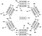
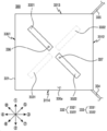
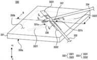
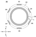
도 1은, 일 실시예에 따른 전자 장치의 분해 사시도 및 결합도이다.
도 2는, 일 실시예에 따른 전자 장치의 일부 구성을 제거한 측면도이다.
도 3a는, 일 실시예에 따른 전자 장치의 안테나 조립체의 정면도이다.
도 3b는, 도 3a의 안테나 조립체의 측면도이다.
도 4는, 일 실시예에 따른 전자 장치 내부의 안테나의 배치 구조를 나타내는 도면이다.
도 5는, 일 실시예에 따른 전자 장치의 안테나와 무선 통신 회로 사이의 전기적 연결 관계를 나타내는 도면이다.
도 6a는, 일 실시예에 따른 전자 장치의 제1 안테나 모듈의 일면을 나타내는 도면이다.
도 6b는, 도 6a의 제1 안테나 모듈의 다른 일면을 나타내는 도면이다.
도 6c는, 도 6a의 제1 안테나 모듈의 사시도이다.
도 6d는, 도 6c의 제1 안테나 모듈을 A-A' 방향으로 절단한 단면도이다.
도 7a는, 일 실시예에 따른 전자 장치의 제3 안테나 모듈의 일면을 나타내는 도면이다.
도 7b는, 도 7a의 제3 안테나 모듈의 다른 일면을 나타내는 도면이다.
도 7c는, 도 7a의 제3 안테나 모듈의 사시도이다.
도 7d는, 도 7c의 제3 안테나 모듈을 B-B' 방향으로 절단한 단면도이다.
도 8a는, 일 실시예에 따른 전자 장치의 제1 주파수 대역에서의 S 파라미터(S parameter)를 나타내는 그래프이다.
도 8b는, 일 실시예에 따른 전자 장치의 제2 주파수 대역 및 제3 주파수 대역에서의 S 파라미터(S parameter)를 나타내는 그래프이다.
도 9a는, 일 실시예에 따른 전자 장치의 내부에 배치되는 유전체를 나타내는 도면이다.
도 9b는, 다른 실시예에 따른 전자 장치의 내부에 배치되는 유전체를 나타내는 도면이다.
도 9c는, 또 다른 실시예에 따른 전자 장치의 내부에 배치되는 유전체를 나타내는 도면이다.
도 10은, 다른 실시예에 따른 전자 장치 내부의 안테나의 배치 구조를 나타내는 도면이다.
도 11은, 다른 실시예에 따른 전자 장치의 안테나와 무선 통신 회로 사이의 전기적 연결 관계를 나타내는 도면이다.
도 12a는, 다른 실시예에 따른 전자 장치의 제1 안테나 모듈의 일면을 나타내는 도면이다.
도 12b는, 도 12a의 제1 안테나 모듈의 다른 일면을 나타내는 도면이다.
도 12c는, 도 12a의 제1 안테나 모듈의 사시도이다.
도 12d는, 도 12c의 제1 안테나 모듈을 C-C' 방향으로 절단한 단면도이다.
도 13은, 다른 실시예에 따른 전자 장치의 안테나 조립체의 정면도이다.
도 14는, 다른 실시예에 따른 전자 장치 내부의 안테나의 배치 구조를 나타내는 도면이다.
도 15는, 다른 실시예에 따른 전자 장치의 안테나와 무선 통신 회로 사이의 전기적 연결 관계를 나타내는 도면이다.
1 is an exploded perspective view and a combined view of an electronic device according to an exemplary embodiment;
2 is a side view with some components removed of an electronic device according to an exemplary embodiment.
3A is a front view of an antenna assembly of an electronic device according to an exemplary embodiment.
3B is a side view of the antenna assembly of FIG. 3A ;
4 is a diagram illustrating an arrangement structure of an antenna inside an electronic device according to an exemplary embodiment.
5 is a diagram illustrating an electrical connection relationship between an antenna of an electronic device and a wireless communication circuit according to an exemplary embodiment.
6A is a diagram illustrating one surface of a first antenna module of an electronic device according to an exemplary embodiment.
FIG. 6B is a diagram illustrating another surface of the first antenna module of FIG. 6A .
6C is a perspective view of the first antenna module of FIG. 6A .
FIG. 6D is a cross-sectional view of the first antenna module of FIG. 6C taken in the AA′ direction.
7A is a diagram illustrating one surface of a third antenna module of an electronic device according to an exemplary embodiment.
FIG. 7B is a diagram illustrating another surface of the third antenna module of FIG. 7A .
7C is a perspective view of the third antenna module of FIG. 7A .
7D is a cross-sectional view of the third antenna module of FIG. 7C taken in the BB' direction.
8A is a graph illustrating an S parameter in a first frequency band of an electronic device according to an exemplary embodiment.
8B is a graph illustrating an S parameter in a second frequency band and a third frequency band of an electronic device according to an exemplary embodiment.
9A is a diagram illustrating a dielectric disposed inside an electronic device according to an exemplary embodiment.
9B is a diagram illustrating a dielectric disposed inside an electronic device according to another exemplary embodiment.
9C is a diagram illustrating a dielectric disposed inside an electronic device according to another exemplary embodiment.
10 is a diagram illustrating an arrangement structure of an antenna inside an electronic device according to another exemplary embodiment.
11 is a diagram illustrating an electrical connection relationship between an antenna of an electronic device and a wireless communication circuit according to another exemplary embodiment.
12A is a diagram illustrating one surface of a first antenna module of an electronic device according to another exemplary embodiment.
12B is a diagram illustrating another surface of the first antenna module of FIG. 12A .
12C is a perspective view of the first antenna module of FIG. 12A .
12D is a cross-sectional view of the first antenna module of FIG. 12C taken in the CC' direction.
13 is a front view of an antenna assembly of an electronic device according to another embodiment.
14 is a diagram illustrating an arrangement structure of an antenna inside an electronic device according to another exemplary embodiment.
15 is a diagram illustrating an electrical connection relationship between an antenna of an electronic device and a wireless communication circuit according to another exemplary embodiment.

본 문서의 다양한 실시예들 및 이에 사용된 용어들은 본 문서에 기재된 기술적 특징들을 특정한 실시예들로 한정하려는 것이 아니며, 해당 실시예의 다양한 변경, 균등물, 또는 대체물을 포함하는 것으로 이해되어야 한다. 도면의 설명과 관련하여, 유사한 또는 관련된 구성요소에 대해서는 유사한 참조 부호가 사용될 수 있다. 아이템에 대응하는 명사의 단수 형은 관련된 문맥상 명백하게 다르게 지시하지 않는 한, 상기 아이템 한 개 또는 복수 개를 포함할 수 있다. 본 문서에서, "A 또는 B", "A 및 B 중 적어도 하나","A 또는 B 중 적어도 하나", "A, B 또는 C", "A, B 및 C 중 적어도 하나" 및 "A, B, 또는 C 중 적어도 하나"와 같은 문구들 각각은 그 문구들 중 해당하는 문구에 함께 나열된 항목들 중 어느 하나, 또는 그들의 모든 가능한 조합을 포함할 수 있다. "제 1", "제 2", 또는 "첫째" 또는 "둘째"와 같은 용어들은 단순히 해당 구성요소를 다른 해당 구성요소와 구분하기 위해 사용될 수 있으며, 해당 구성요소들을 다른 측면(예: 중요성 또는 순서)에서 한정하지 않는다. 어떤(예: 제 1) 구성요소가 다른(예: 제 2) 구성요소에, "기능적으로" 또는 "통신적으로"라는 용어와 함께 또는 이런 용어 없이, "커플드" 또는 "커넥티드"라고 언급된 경우, 그것은 상기 어떤 구성요소가 상기 다른 구성요소에 직접적으로(예: 유선으로), 무선으로, 또는 제 3 구성요소를 통하여 연결될 수 있다는 것을 의미한다. 이하 본 개시의 다양한 실시예를 첨부된 도면을 참조하여 상세히 설명한다.It should be understood that the various embodiments of this document and the terms used therein are not intended to limit the technical features described in this document to specific embodiments, and include various modifications, equivalents, or substitutions of the embodiments. In connection with the description of the drawings, like reference numerals may be used for similar or related components. The singular form of the noun corresponding to the item may include one or more of the item, unless the relevant context clearly dictates otherwise. As used herein, "A or B", "at least one of A and B", "at least one of A or B", "A, B or C", "at least one of A, B and C" and "A; Each of the phrases "at least one of B, or C" may include any one of, or all possible combinations of, items listed together in the corresponding one of the phrases. Terms such as “first”, “second”, or “first” or “second” may simply be used to distinguish the component from other components in question, and may refer to components in other aspects (e.g., importance or order) is not limited. It is said that one (eg, first) component is "coupled" or "connected" to another (eg, second) component, with or without the terms "functionally" or "communicatively". When referenced, it means that one component can be connected to the other component directly (eg by wire), wirelessly, or through a third component. Hereinafter, various embodiments of the present disclosure will be described in detail with reference to the accompanying drawings.

도 1은, 일 실시예에 따른 전자 장치(100)의 분해 사시도 및 결합도이고, 도 2는, 일 실시예에 따른 전자 장치(100)의 일부 구성(예: 측면 커버(112))을 제거한 측면도이다. 도 2는 도 1의 전자 장치(100)를 -y 방향에서 바라본 전자 장치(100)의 측면을 나타내는 도면이다.1 is an exploded perspective view and a combined view of an electronic device 100 according to an embodiment, and FIG. 2 is an exploded perspective view of an electronic device 100 according to an embodiment. It is a side view. FIG. 2 is a diagram illustrating a side surface of the electronic device 100 of FIG. 1 when viewed from the -y direction.

도 1 및 도 2를 참조하면, 일 실시예에 따른 전자 장치(100)는, 하우징(110), 적어도 하나의 인쇄 회로 기판(120), 적어도 하나의 방열판(130), 전원 보드(140), 안테나 조립체(200)를 포함할 수 있다. 본 개시의 일 실시예에 따른 전자 장치(100)는, 예를 들어, 액세스 포인트(AP: access point)일 수 있으나, 이에 한정되는 것은 아니다.1 and 2 , an electronic device 100 according to an embodiment includes a housing 110 , at least one printed circuit board 120 , at least one heat sink 130 , a power board 140 , An antenna assembly 200 may be included. The electronic device 100 according to an embodiment of the present disclosure may be, for example, an access point (AP), but is not limited thereto.

일 실시예에 따르면, 하우징(110)은 상단 커버(111), 측면 커버(112), 고정 부재(113)를 포함하고, 전자 장치(100)의 외관을 형성할 수 있다. 일 예시에서, 상단 커버(111)는 전자 장치(100)의 제1 방향(예: (예: 도 1의 +z 방향)을 향하는 제1 면(또는 "상단면")을 형성할 수 있고, 고정 부재(113)는 제1 방향과 반대 방향(예: 도 1의 -z 방향)을 향하는 제2 면(또는 "하단면")을 형성할 수 있으며, 측면 커버(112)는 제1 면 및/또는 제2 면과 수직한 제3 면(또는 "측면")을 형성할 수 있다. 일 예시에서, 상단 커버(111), 측면 커버(112), 및 고정 부재(113)에 의해 하우징(110) 내부에는 공간(도 2의 A 영역)(이하 "내부 공간")이 형성될 수 있으며, 내부 공간(A)에는 전자 장치(100)의 구성 요소들(예: 적어도 하나의 인쇄 회로 기판(120), 적어도 하나의 방열판(130), 전원 보드(140), 및/또는 안테나 조립체(200))이 배치될 수 있다. 일 예시에서, 상단 커버(111) 및/또는 측면 커버(112)는 상단 커버(111), 측면 커버(112) 및 고정 부재(113)에 의해 하우징(110) 내부에 형성되는 내부 공간(A)에 배치된 전자 장치(100)의 구성 요소들이 외부 충격에 의해 손상되는 것을 방지할 수 있다. 다른 예시에서, 고정 부재(113)는 전자 장치(100)가 지정된 위치(예: 지면)에 고정되도록 할 수 있다. 일 실시예에 따르면, 하우징(110)은 원기둥 형상으로 형성될 수 있으나 이에 한정되는 것은 아니며, 다른 실시예(미도시)에 따른 하우징(110)은 밑면이 다각형인 다각 기둥(예: 삼각 기둥, 및/또는 사각 기둥) 형상으로 형성될 수도 있다.According to an embodiment, the housing 110 may include a top cover 111 , a side cover 112 , and a fixing member 113 , and may form an exterior of the electronic device 100 . In one example, the top cover 111 may form a first surface (or "top surface") facing the first direction (eg, (eg, +z direction in FIG. 1)) of the electronic device 100, The fixing member 113 may form a second surface (or "lower surface") facing the direction opposite to the first direction (eg, -z direction in FIG. 1 ), and the side cover 112 may include the first surface and and/or a third face (or “side”) perpendicular to the second face, in one example, the housing 110 by the top cover 111 , the side cover 112 , and the fixing member 113 . ) A space (region A in FIG. 2 ) (hereinafter, “internal space”) may be formed inside, and components of the electronic device 100 (eg, at least one printed circuit board 120 ) may be formed in the interior space (A). ), at least one heat sink 130 , a power board 140 , and/or an antenna assembly 200. In one example, the top cover 111 and/or the side cover 112 are disposed on the top The components of the electronic device 100 disposed in the inner space A formed inside the housing 110 by the cover 111 , the side cover 112 , and the fixing member 113 are prevented from being damaged by external impact. In another example, the fixing member 113 may allow the electronic device 100 to be fixed to a designated position (eg, the ground). According to an embodiment, the housing 110 may be formed in a cylindrical shape. However, the present invention is not limited thereto, and the housing 110 according to another embodiment (not shown) may be formed in the shape of a polygonal pole (eg, a triangular pole and/or a quadrangular pole) having a polygonal bottom surface.

일 실시예에 따르면, 적어도 하나의 인쇄 회로 기판(120)은 내부 공간(A) 내에 배치될 수 있으며, 적어도 하나의 인쇄 회로 기판(120)에는 전자 장치(100)의 기능을 수행하기 위한 전자 부품들이 배치될 수 있다. 일 예시에서, 적어도 하나의 인쇄 회로 기판(120)에는 무선 통신을 수행하기 위한 무선 통신 회로(예: 도 5의 무선 통신 회로(400))가 배치될 수 있다. 무선 통신 회로는 안테나 조립체(200)의 적어도 하나의 안테나 모듈(300)과 전기적으로 연결되어 RF 신호를 송신 또는 수신할 수 있으며, 이에 대한 설명은 후술하도록 한다. 일 예시에서, 적어도 하나의 인쇄 회로 기판(120)은 복수 개로 구성될 수 있으며, 예를 들어, 제1 인쇄 회로 기판(121) 및 제2 인쇄 회로 기판(122)을 포함할 수 있다. 다른 예시(미도시)에서, 적어도 하나의 인쇄 회로 기판(120)은 하나의 인쇄 회로 기판으로 구성될 수도 있다.According to an embodiment, the at least one printed circuit board 120 may be disposed in the inner space A, and the at least one printed circuit board 120 includes an electronic component for performing a function of the electronic device 100 . can be placed. In one example, a wireless communication circuit (eg, the wireless communication circuit 400 of FIG. 5 ) for performing wireless communication may be disposed on the at least one printed circuit board 120 . The wireless communication circuit may be electrically connected to at least one antenna module 300 of the antenna assembly 200 to transmit or receive an RF signal, and a description thereof will be provided later. In one example, the at least one printed circuit board 120 may be configured in plurality, and may include, for example, a first printed circuit board 121 and a second printed circuit board 122 . In another example (not shown), the at least one printed circuit board 120 may be configured as one printed circuit board.

일 실시예에 따르면, 적어도 하나의 방열판(130)은 전자 장치(100)의 내부 공간(A)에서 발생되는 열을 방열할 수 있다. 일 예시에서, 적어도 하나의 방열판(130)은 적어도 하나의 인쇄 회로 기판(120)과 인접한 위치에 배치되어, 적어도 하나의 인쇄 회로 기판(120)에 배치된 전자 부품들의 작동 과정에서 발생되는 열을 방열할 수 있다. 예를 들어, 적어도 하나의 인쇄 회로 기판(120)에 배치된 무선 통신 회로와 안테나 조립체(200)의 적어도 하나의 안테나 모듈(300) 사이에서 RF 신호가 송신 또는 수신되는 과정에서 열이 발생할 수 있으며, 적어도 하나의 방열판(130)은 무선 통신 회로에 의해 발생된 열을 방열할 수 있다. 일 예시에서, 적어도 하나의 방열판(130)은 제1 인쇄 회로 기판(121)과 제2 인쇄 회로 기판(122) 사이에 배치되는 제1 방열판(131) 및 제1 인쇄 회로 기판(121)과 인접한 제2 방열판(132)을 포함할 수 있다. 다만, 상술한 실시예에 한정되는 것은 아니며, 실시예에 따라 적어도 하나의 방열판(130)은 하나의 방열판으로 구성되거나, 복수 개(예: 3개, 4개 또는 4개 이상)의 방열판으로 구성될 수도 있다.According to an embodiment, the at least one heat sink 130 may radiate heat generated in the internal space A of the electronic device 100 . In one example, the at least one heat sink 130 is disposed adjacent to the at least one printed circuit board 120 to dissipate heat generated during the operation of electronic components disposed on the at least one printed circuit board 120 . can heat up. For example, heat may be generated in the process of transmitting or receiving an RF signal between the wireless communication circuit disposed on the at least one printed circuit board 120 and the at least one antenna module 300 of the antenna assembly 200, , the at least one heat sink 130 may dissipate heat generated by the wireless communication circuit. In one example, the at least one heat sink 130 is adjacent to the first heat sink 131 and the first printed circuit board 121 disposed between the first printed circuit board 121 and the second printed circuit board 122 . A second heat sink 132 may be included. However, it is not limited to the above-described embodiment, and according to the embodiment, at least one heat sink 130 is composed of one heat sink or a plurality of heat sinks (eg, 3, 4, or 4 or more). could be

일 실시예에 따르면, 전원 보드(140)는 내부 공간(A) 내에 배치되어, 전자 장치(100)의 구성 요소들에 전원을 공급할 수 있다. 일 예시에서, 전원 보드(140)는 적어도 하나의 인쇄 회로 기판(120)에 배치된 무선 통신 회로와 전기적으로 연결될 수 있고, 그 결과 전원 보드(140)는 무선 통신 회로에 전원을 공급할 수 있다.According to an embodiment, the power board 140 may be disposed in the internal space A to supply power to components of the electronic device 100 . In one example, the power board 140 may be electrically connected to a wireless communication circuit disposed on the at least one printed circuit board 120 , and as a result, the power board 140 may supply power to the wireless communication circuit.

일 실시예에 따르면, 안테나 조립체(200)는 내부 공간(A) 내에 배치되고, 고정 브라켓(210) 및/또는 적어도 하나의 안테나 모듈(300)를 포함할 수 있다. 일 예시에서, 고정 브라켓(210)은 내부 공간(A)의 상단 영역(예: 도 1, 도 2의 +z 방향의 영역)에 배치되어, 적어도 하나의 안테나 모듈(300)을 내부 공간(A)의 상단 영역에 고정시킬 수 있다. 예를 들어, 고정 브라켓(210)의 일 영역에는 적어도 하나의 고정 홈(미도시)이 형성될 수 있으며, 적어도 하나의 안테나 모듈(300)은 고정 브라켓(210)의 적어도 하나의 고정 홈에 위치함으로써, 내부 공간(A)의 상단 영역에 고정될 수 있다. 일 실시예에 따른 전자 장치(100)에서는, 적어도 하나의 안테나 모듈(300)이 적어도 하나의 다른 전자 부품들(예: 적어도 하나의 인쇄 회로 기판(120), 적어도 하나의 방열판(130) 및/또는 전원 보드(140))의 상단(예: 도 2의 +z 방향)에 위치함으로써, 다른 전자 부품들에 의한 안테나(300)의 방사 성능 열화를 줄일 수 있다.According to an embodiment, the antenna assembly 200 is disposed in the inner space A, and may include a fixing bracket 210 and/or at least one antenna module 300 . In one example, the fixing bracket 210 is disposed in the upper area (eg, the area in the +z direction of FIGS. 1 and 2) of the inner space (A), at least one antenna module 300 is installed in the inner space (A) ) can be fixed to the upper area of the For example, at least one fixing groove (not shown) may be formed in one region of the fixing bracket 210 , and the at least one antenna module 300 is positioned in the at least one fixing groove of the fixing bracket 210 . By doing so, it can be fixed to the upper region of the inner space (A). In the electronic device 100 according to an embodiment, at least one antenna module 300 includes at least one other electronic component (eg, at least one printed circuit board 120 , at least one heat sink 130 , and/or Alternatively, by being positioned at the upper end (eg, in the +z direction in FIG. 2 ) of the power board 140 , deterioration in radiation performance of the antenna 300 due to other electronic components may be reduced.

일 예시에서, 적어도 하나의 안테나 모듈(300)은 무선 통신 회로(예: 도 5의 무선 통신 회로(400))와 전기적으로 연결될 수 있다. 이에 따라, 적어도 하나의 안테나 모듈(300)은 적어도 하나의 외부 전자 장치(미도시)로 지정된 주파수 대역의 RF 신호를 송신하거나, 적어도 하나의 외부 전자 장치로부터 지정된 주파수 대역의 RF 신호를 수신할 수 있다. 다만, 적어도 하나의 안테나 모듈(300)의 구성 및 무선 통신 회로와의 전기적 연결 관계에 대한 구체적인 설명은 후술하도록 한다. In one example, the at least one antenna module 300 may be electrically connected to a wireless communication circuit (eg, the wireless communication circuit 400 of FIG. 5 ). Accordingly, at least one antenna module 300 may transmit an RF signal of a specified frequency band to at least one external electronic device (not shown) or receive an RF signal of a specified frequency band from at least one external electronic device. have. However, a detailed description of the configuration of the at least one antenna module 300 and an electrical connection relationship with the wireless communication circuit will be described later.

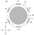
도 3a는, 일 실시예에 따른 전자 장치의 안테나 조립체(200)의 정면도이고, 도 3b는, 도 3a의 안테나 조립체(200)의 측면도이다. 도 3a는 도 1 및/또는 도 2의 안테나 조립체(200)를 도 1 및/또는 도 2의 +z 방향에서 바라본 도면이고, 도 3b는 도 1 및/또는 도 2의 안테나 조립체(200)를 도 1 및/또는 도 2의 -y 방향에서 바라본 도면이다.3A is a front view of the antenna assembly 200 of an electronic device according to an exemplary embodiment, and FIG. 3B is a side view of the antenna assembly 200 of FIG. 3A . 3A is a view of the antenna assembly 200 of FIGS. 1 and/or 2 as viewed in the +z direction of FIGS. 1 and/or 2, and FIG. 3B is the antenna assembly 200 of FIGS. 1 and/or 2 It is a view viewed from the -y direction of FIGS. 1 and/or 2 .

도 3a 및 도 3b를 참조하면, 일 실시예에 따른 전자 장치의 안테나 조립체(200)는, 고정 브라켓(210)(예: 도 2의 고정 브라켓(210)) 및 적어도 하나의 안테나 모듈(310, 320, 330, 340, 350 및/또는 360)(예: 도 2의 적어도 하나의 안테나 모듈(300))을 포함할 수 있다.3A and 3B , the antenna assembly 200 of the electronic device according to an embodiment includes a fixing bracket 210 (eg, the fixing bracket 210 of FIG. 2 ) and at least one antenna module 310; 320, 330, 340, 350, and/or 360 (eg, at least one antenna module 300 of FIG. 2).

일 실시예에 따르면, 고정 브라켓(210)은 적어도 하나의 안테나 모듈(310, 320, 330, 340, 350 및/또는 360)을 고정시키기 위한 적어도 하나의 고정 홈(220)을 포함할 수 있다. 일 예시에서, 적어도 하나의 고정 홈(220)은 제1 고정 홈(221), 제2 고정 홈(222), 제3 고정 홈(223), 제4 고정 홈(224), 제5 고정 홈(225), 및/또는 제6 고정 홈(226)을 포함할 수 있다. 제1 고정 홈(221), 제2 고정 홈(222), 제3 고정 홈(223), 제4 고정 홈(224), 제5 고정 홈(225) 및/또는 제6 고정 홈(226)은 고정 브라켓(210)의 가상의 중심(도 3a의 M)을 기준으로 방사형으로 배치될 수 있다. 예를 들어, 고정 브라켓(210)의 가상의 중심(M)을 기준으로, 제1 고정 홈(221)과 제2 고정 홈(222)이 서로 대칭되도록 배치되고, 제3 고정 홈(223)과 제4 고정 홈(224)이 서로 대칭되도록 배치되고, 제5 고정 홈(225)과 제6 고정 홈(226)이 서로 대칭되도록 배치될 수 있다.According to an embodiment, the fixing bracket 210 may include at least one fixing groove 220 for fixing the at least one antenna module 310 , 320 , 330 , 340 , 350 and/or 360 . In one example, the at least one fixing groove 220 includes a first fixing groove 221 , a second fixing groove 222 , a third fixing groove 223 , a fourth fixing groove 224 , and a fifth fixing groove ( 225 ), and/or a sixth fixing groove 226 . The first fixing groove 221 , the second fixing groove 222 , the third fixing groove 223 , the fourth fixing groove 224 , the fifth fixing groove 225 and/or the sixth fixing groove 226 are It may be radially disposed based on the virtual center (M of FIG. 3A ) of the fixing bracket 210 . For example, based on the imaginary center M of the fixing bracket 210 , the first fixing groove 221 and the second fixing groove 222 are symmetrical to each other, and the third fixing groove 223 and the The fourth fixing groove 224 may be symmetrical to each other, and the fifth fixing groove 225 and the sixth fixing groove 226 may be symmetrical to each other.

일 실시예에 따르면, 적어도 하나의 안테나 모듈(310, 320, 330, 340, 350 및/또는 360)은 고정 브라켓(210)의 적어도 하나의 고정 홈(220)에 배치되어, 다양한 주파수 대역의 RF 신호를 송신 또는 수신하는 안테나 방사체로 동작할 수 있다. 일 예시에서, 적어도 하나의 안테나 모듈(310, 320, 330, 340, 350 및/또는 360)은, 제1 고정 홈(221)에 배치되는 제1 안테나 모듈(310), 제2 고정 홈(222)에 배치되는 제2 안테나 모듈(320), 제3 고정 홈(223)에 배치되는 제3 안테나 모듈(330), 제4 고정 홈(224)에 배치되는 제4 안테나 모듈(340), 제5 고정 홈(225)에 배치되는 제5 안테나 모듈(350), 및/또는 제6 고정 홈(226)에 배치되는 제6 안테나 모듈(360)을 포함할 수 있다.According to one embodiment, at least one antenna module (310, 320, 330, 340, 350 and/or 360) is disposed in at least one fixing groove 220 of the fixing bracket 210, RF of various frequency bands It can operate as an antenna radiator that transmits or receives a signal. In one example, the at least one antenna module 310 , 320 , 330 , 340 , 350 and/or 360 includes a first antenna module 310 disposed in a first fixing groove 221 , a second fixing groove 222 . ), the second antenna module 320 disposed in the third fixing groove 223 , the third antenna module 330 disposed in the fourth fixing groove 224 , the fourth antenna module 340 disposed in the fourth fixing groove 224 , the fifth It may include a fifth antenna module 350 disposed in the fixing groove 225 , and/or a sixth antenna module 360 disposed in the sixth fixing groove 226 .

일 예시에서, 제1 안테나 모듈(310), 제2 안테나 모듈(320), 제3 안테나 모듈(330), 제4 안테나 모듈(340), 제5 안테나 모듈(350), 및/또는 제6 안테나 모듈(360)은, 상술한 적어도 하나의 고정 홈(220)(예: 제1 고정 홈(221), 제2 고정 홈(222), 제3 고정 홈(223), 제4 고정 홈(224), 제5 고정 홈(225), 및/또는 제6 고정 홈(226))의 배치 구조를 통해 고정 브라켓(210)의 가상의 중심(M)을 기준으로 방사형으로 배치될 수 있다. 예를 들어, 고정 브라켓(210)의 가상의 중심(M)을 기준으로 제1 안테나 모듈(310)의 일면과 제2 안테나 모듈(320)의 일면이 서로 마주보도록 배치될 수 있다. 다른 예시에서, 고정 브라켓(210)의 가상의 중심(M)을 기준으로 제3 안테나 모듈(330)의 일면과 제4 안테나 모듈(340)의 일면이 서로 마주보도록 배치될 수 있다. 또 다른 예시에서, 고정 브라켓(210)의 가상의 중심(M)을 기준으로 제5 안테나 모듈(350)의 일면과 제6 안테나 모듈(360)의 일면이 서로 마주보도록 배치될 수 있다. 일 예시에서, 제1 안테나 모듈(310), 제2 안테나 모듈(320), 제3 안테나 모듈(330), 제4 안테나 모듈(340), 제5 안테나 모듈(350) 및/또는 제6 안테나 모듈(360)은 고정 브라켓(210)의 가상의 중심(M)을 기준으로 동일한 간격으로 배치될 수 있다. 예를 들어, 제1 안테나 모듈(310), 제2 안테나 모듈(320), 제3 안테나 모듈(330), 제4 안테나 모듈(340), 제5 안테나 모듈(350) 및/또는 제6 안테나 모듈(360)은 고정 브라켓(210)의 가상의 중심(M)을 기준으로 60˚ 간격으로 배치될 수 있다. 다만, 제1 안테나 모듈(310), 제2 안테나 모듈(320), 제3 안테나 모듈(330), 제4 안테나 모듈(340), 제5 안테나 모듈(350) 및/또는 제6 안테나 모듈(360)의 배치 위치가 상술한 실시예에 한정되는 것은 아니며, 다른 실시예에 따르면, 제1 안테나 모듈(310), 제2 안테나 모듈(320), 제3 안테나 모듈(330), 제4 안테나 모듈(340), 제5 안테나 모듈(350) 및/또는 제6 안테나 모듈(360)은 불규칙한 간격으로 배치될 수도 있다.In one example, the first antenna module 310 , the second antenna module 320 , the third antenna module 330 , the fourth antenna module 340 , the fifth antenna module 350 , and/or the sixth antenna The module 360 includes at least one of the above-described fixing grooves 220 (eg, the first fixing groove 221 , the second fixing groove 222 , the third fixing groove 223 , and the fourth fixing groove 224 ). , the fifth fixing groove 225 , and/or the sixth fixing groove 226) may be radially disposed based on the virtual center M of the fixing bracket 210 through the arrangement structure. For example, one surface of the first antenna module 310 and one surface of the second antenna module 320 may be disposed to face each other based on the virtual center M of the fixing bracket 210 . In another example, one surface of the third antenna module 330 and one surface of the fourth antenna module 340 may be disposed to face each other based on the virtual center M of the fixing bracket 210 . In another example, one surface of the fifth antenna module 350 and one surface of the sixth antenna module 360 may be disposed to face each other based on the virtual center M of the fixing bracket 210 . In one example, the first antenna module 310 , the second antenna module 320 , the third antenna module 330 , the fourth antenna module 340 , the fifth antenna module 350 and/or the sixth antenna module 360 may be arranged at equal intervals based on the virtual center (M) of the fixing bracket (210). For example, the first antenna module 310 , the second antenna module 320 , the third antenna module 330 , the fourth antenna module 340 , the fifth antenna module 350 and/or the sixth antenna module 360 may be arranged at intervals of 60˚ based on the virtual center (M) of the fixing bracket (210). However, the first antenna module 310 , the second antenna module 320 , the third antenna module 330 , the fourth antenna module 340 , the fifth antenna module 350 and/or the sixth antenna module 360 . ) is not limited to the above embodiment, and according to another embodiment, the first antenna module 310, the second antenna module 320, the third antenna module 330, the fourth antenna module ( 340), the fifth antenna module 350, and/or the sixth antenna module 360 may be arranged at irregular intervals.

일 실시예에 따르면, 적어도 하나의 안테나 모듈(310, 320, 330, 340, 350 및/또는 360)은 일면에 배치되는 도전성 패턴과 상기 일면과 반대 방향을 향하는 타면에 배치되는 도전성 패턴을 포함할 수 있다. 예를 들어, 제1 안테나 모듈(310)는 제1 안테나 모듈(310)의 일면에 배치되는 제1 도전성 패턴(미도시) 및/또는 상술한 제1 안테나 모듈(310)의 일면과 반대 방향을 향하는 타면에 배치되는 제2 도전성 패턴(미도시)를 포함할 수 있다.According to one embodiment, the at least one antenna module (310, 320, 330, 340, 350 and/or 360) may include a conductive pattern disposed on one surface and a conductive pattern disposed on the other surface facing the opposite direction to the one surface. can For example, the first antenna module 310 has a direction opposite to the first conductive pattern (not shown) disposed on one surface of the first antenna module 310 and/or one surface of the above-described first antenna module 310 . It may include a second conductive pattern (not shown) disposed on the other surface facing.

일 예시에서, 적어도 하나의 안테나 모듈(310, 320, 330, 340, 350 및/또는 360)의 일면 및/또는 타면에 배치되는 도전성 패턴들은 무선 통신 회로(예: 도 5의 무선 통신 회로(400))와 전기적으로 연결되어, 안테나 방사체로 동작할 수 있다. 예를 들어, 무선 통신 회로는 적어도 하나의 안테나 모듈(310, 320, 330, 340, 350 및/또는 360)의 일면 및/또는 타면에 배치되는 도전성 패턴들에 지정된 주파수 대역의 RF 신호를 송신 또는 급전(feeding)할 수 있다. 다른 예시로, 무선 통신 회로는 적어도 하나의 안테나 모듈(310, 320, 330, 340, 350 및/또는 360)의 일면 및/또는 타면에 배치되는 도전성 패턴들로부터 지정된 주파수 대역의 RF 신호를 수신할 수 있다. 예를 들어, 제1 안테나 모듈(310)의 제1 도전성 패턴 및/또는 제2 도전성 패턴은 무선 통신 회로와 전기적으로 연결되어, 지정된 주파수 대역의 RF 신호를 송신 또는 수신하는 안테나 방사체로 동작할 수 있다. 적어도 하나의 안테나 모듈(310, 320, 330, 340, 350 및/또는 360)의 구성 및 무선 통신 회로와 적어도 하나의 안테나 모듈(310, 320, 330, 340, 350 및/또는 360)의 전기적 연결 관계에 대한 설명은 후술하도록 한다.In one example, conductive patterns disposed on one side and/or the other side of the at least one antenna module 310 , 320 , 330 , 340 , 350 and/or 360 may include a wireless communication circuit (eg, the wireless communication circuit 400 of FIG. 5 ). )) and electrically connected to it, it can operate as an antenna radiator. For example, the wireless communication circuit transmits or receives an RF signal of a frequency band specified in conductive patterns disposed on one and/or the other surface of the at least one antenna module 310 , 320 , 330 , 340 , 350 and/or 360 . can be fed. As another example, the wireless communication circuit may receive an RF signal of a specified frequency band from conductive patterns disposed on one side and/or the other side of at least one antenna module (310, 320, 330, 340, 350 and/or 360). can For example, the first conductive pattern and/or the second conductive pattern of the first antenna module 310 may be electrically connected to a wireless communication circuit to operate as an antenna radiator for transmitting or receiving RF signals of a specified frequency band. have. Configuration of at least one antenna module (310, 320, 330, 340, 350 and/or 360) and electrical connection of at least one antenna module (310, 320, 330, 340, 350 and/or 360) with a wireless communication circuit A description of the relationship will be provided later.

도 4는, 일 실시예에 따른 전자 장치(100) 내부의 안테나(예: 적어도 하나의 안테나 모듈(310, 320, 330, 340, 350 및/또는 360))의 배치 구조를 나타내는 도면이고, 도 5는, 일 실시예에 따른 전자 장치(100)의 안테나(예: 적어도 하나의 안테나 모듈(310, 320, 330, 340, 350 및/또는 360))와 무선 통신 회로(400) 사이의 전기적 연결 관계를 나타내는 도면이다. 도 4는 도 3a의 안테나 조립체(200)에서 고정 브라켓(210)을 제거한 상태를 나타내는 도면이다.4 is a diagram illustrating an arrangement structure of an antenna (eg, at least one antenna module 310 , 320 , 330 , 340 , 350 and/or 360 ) inside the electronic device 100 according to an embodiment; 5, an electrical connection between an antenna (eg, at least one antenna module 310 , 320 , 330 , 340 , 350 and/or 360 ) of the electronic device 100 and the wireless communication circuit 400 according to an embodiment It is a diagram showing the relationship. FIG. 4 is a view showing a state in which the fixing bracket 210 is removed from the antenna assembly 200 of FIG. 3A .

도 4 및 도 5를 참조하면, 일 실시예에 따른 전자 장치(100)(예: 도 1의 전자 장치(100))는, 적어도 하나의 안테나 모듈(310, 320, 330, 340, 350 및/또는 360)(예: 도 3a, 도 3b의 적어도 하나의 안테나 모듈(310, 320, 330, 340, 350 및/또는 360)), 무선 통신 회로(400)를 포함할 수 있다.4 and 5 , the electronic device 100 (eg, the electronic device 100 of FIG. 1 ) according to an embodiment includes at least one antenna module 310 , 320 , 330 , 340 , 350 and/or or 360) (eg, at least one antenna module 310 , 320 , 330 , 340 , 350 and/or 360 of FIGS. 3A and 3B ), and a wireless communication circuit 400 .

일 실시예에 따르면, 적어도 하나의 안테나 모듈(310, 320, 330, 340, 350 및/또는 360)은 제1 안테나 모듈(310)(예: 도 3a의 제1 안테나 모듈(310)), 제2 안테나 모듈(320)(예: 도 3a의 제2 안테나 모듈(320)), 제3 안테나 모듈(330)(예: 도 3a의 제3 안테나 모듈(330)), 제4 안테나 모듈(340)(예: 도 3a의 제4 안테나 모듈(340)), 제5 안테나 모듈(350)(예: 도 3a의 제5 안테나 모듈(350)), 및/또는 제6 안테나 모듈(360)(예: 도 3a의 제6 안테나 모듈(360))을 포함할 수 있다. 일 예시에서, 제1 안테나 모듈(310), 제2 안테나 모듈(320), 제3 안테나 모듈(330), 제4 안테나 모듈(340), 제5 안테나 모듈(350) 및/또는 제6 안테나 모듈(360)은 가상의 중심(M)(예: 도 3a의 가상의 중심(M))을 기준으로 방사형으로 배치될 수 있다. 예를 들어, 제1 안테나 모듈(310)은 제2 안테나 모듈(320)와 서로 마주 보도록 배치되고, 제3 안테나 모듈(330)은 제4 안테나 모듈(340)와 서로 마주보도록 배치되며, 제5 안테나 모듈(350)은 제6 안테나 모듈(360)와 서로 마주보도록 배치될 수 있다. 일 예시에서, 제1 안테나 모듈(310), 제2 안테나 모듈(320), 제3 안테나 모듈(330), 제4 안테나 모듈(340), 제5 안테나 모듈(350) 및/또는 제6 안테나 모듈(360)은 가상의 중심(M)을 기준으로 동일한 간격으로 배치될 수 있다. 예를 들어, 제1 안테나 모듈(310), 제2 안테나 모듈(320), 제3 안테나 모듈(330), 제4 안테나 모듈(340), 제5 안테나 모듈(350) 및/또는 제6 안테나 모듈(360)은 가상의 중심(M)을 기준으로 60˚ 간격으로 배치될 수 있다. 다만, 제1 안테나 모듈(310), 제2 안테나 모듈(320), 제3 안테나 모듈(330), 제4 안테나 모듈(340), 제5 안테나 모듈(350) 및/또는 제6 안테나 모듈(360)의 배치 위치가 상술한 실시예에 한정되는 것은 아니며, 다른 실시예에 따르면, 제1 안테나 모듈(310), 제2 안테나 모듈(320), 제3 안테나 모듈(330), 제4 안테나 모듈(340), 제5 안테나 모듈(350) 및/또는 제6 안테나 모듈(360)은 불규칙한 간격으로 배치될 수도 있다.According to an embodiment, the at least one antenna module 310 , 320 , 330 , 340 , 350 and/or 360 includes the first antenna module 310 (eg, the first antenna module 310 of FIG. 3A ), the second 2 antenna module 320 (eg, the second antenna module 320 of FIG. 3A ), the third antenna module 330 (eg, the third antenna module 330 of FIG. 3A ), the fourth antenna module 340 ) (eg, the fourth antenna module 340 of FIG. 3A ), the fifth antenna module 350 (eg, the fifth antenna module 350 of FIG. 3A ), and/or the sixth antenna module 360 (eg: The sixth antenna module 360 of FIG. 3A may be included. In one example, the first antenna module 310 , the second antenna module 320 , the third antenna module 330 , the fourth antenna module 340 , the fifth antenna module 350 and/or the sixth antenna module 360 may be radially disposed based on the virtual center M (eg, the virtual center M of FIG. 3A ). For example, the first antenna module 310 is disposed to face each other with the second antenna module 320 , the third antenna module 330 is disposed to face each other with the fourth antenna module 340 , and the fifth antenna module 330 is disposed to face each other. The antenna module 350 may be disposed to face the sixth antenna module 360 . In one example, the first antenna module 310 , the second antenna module 320 , the third antenna module 330 , the fourth antenna module 340 , the fifth antenna module 350 and/or the sixth antenna module 360 may be arranged at the same interval based on the virtual center (M). For example, the first antenna module 310 , the second antenna module 320 , the third antenna module 330 , the fourth antenna module 340 , the fifth antenna module 350 and/or the sixth antenna module (360) may be arranged at intervals of 60˚ based on the virtual center (M). However, the first antenna module 310 , the second antenna module 320 , the third antenna module 330 , the fourth antenna module 340 , the fifth antenna module 350 and/or the sixth antenna module 360 . ) is not limited to the above embodiment, and according to another embodiment, the first antenna module 310, the second antenna module 320, the third antenna module 330, the fourth antenna module ( 340), the fifth antenna module 350, and/or the sixth antenna module 360 may be arranged at irregular intervals.

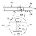
일 실시예에 따르면, 제1 안테나 모듈(310)은, 제1 유전체 기판(311), 제1 도전성 패턴(312) 및/또는 제2 도전성 패턴(313)을 포함할 수 있다. 일 예시에서, 제1 유전체 기판(311)은 지정된 유전율을 갖는 재질로 형성되는 기판일 수 있으며, 제1 유전체 기판(311)은 제1 면(310a) 및 제1 면(310a)과 반대 방향을 향하는 제2 면(310b)을 포함할 수 있다. 예를 들어, 제1 유전체 기판(311)은 유리 에폭시 재질(예: FR4 재질 및/또는 CEM-1 재질) 및/또는 PP(paper phenol) 재질로 형성될 수 있으나, 이에 한정되는 것은 아니다. 일 예시에서, 제1 도전성 패턴(312)은 제1 유전체 기판(311)의 제1 면(310a)에 위치하고, 제1 주파수 대역의 RF 신호를 송신 또는 수신하는 안테나 방사체로 동작할 수 있다. 예를 들어, 제1 도전성 패턴(312)은 무선 통신 회로(400)와 전기적으로 연결될 수 있으며, 제1 도전성 패턴(312)과 무선 통신 회로(400) 사이에는 제1 주파수 대역의 RF 신호가 송신 또는 수신될 수 있다. 예를 들어, 제1 주파수 대역은, 약 2.4 GHz 내지 약 2.5 GHz 주파수 대역일 수 있다. 일 예시에서, 제2 도전성 패턴(313)은 제1 유전체 기판(311)의 제2 면(310b)에 위치하고, 제1 도전성 패턴(312)과 실질적으로 동일 또는 유사하게 제1 주파수 대역의 RF 신호를 송신 또는 수신하는 안테나 방사체로 동작할 수 있다. 예를 들어, 제2 도전성 패턴(313)은 무선 통신 회로(400)와 전기적으로 연결될 수 있으며, 제2 도전성 패턴(313)과 무선 통신 회로(400) 사이에는 제1 주파수 대역의 RF 신호가 송신 또는 수신될 수 있다. 일 예시에서, 제1 안테나 모듈(310)은 제1 유전체 기판(311)의 제1 면(310a)에 제1 도전성 패턴(312)이 배치되고, 제1 유전체 기판(311)의 제2 면(310b)에 제2 도전성 패턴(313)이 배치됨에 따라, 전자 장치(100) 내에 제1 주파수 대역의 RF 신호를 송신 및/또는 수신하는 안테나가 2개 배치된 것과 실질적으로 동일한 효과를 구현할 수 있다. 다른 예시에서, 제1 도전성 패턴(312)과 제2 도전성 패턴(313)이 동일한 제1 주파수 대역의 RF 신호를 송신 및/또는 수신하는 안테나 방사체로 동작함에 따라, 제1 도전성 패턴(312)은 제2 도전성 패턴(313)과 실질적으로 수직을 이루도록 배치될 수 있다. 예를 들어, 제1 도전성 패턴(312)과 제2 도전성 패턴(313)이 이루는 각도가 실질적으로 수직일 수 있다. 제1 도전성 패턴(312)과 제2 도전성 패턴(313)이 실질적으로 수직하게 배치됨에 따라, 제1 도전성 패턴(312)에서 방사되는 RF 신호와 제2 도전성 패턴(313)에서 방사되는 RF 신호 사이의 아이솔레이션(isolation)이 확보될 수 있다. 다만, 이에 대한 구체적인 설명은 후술하도록 한다.According to an embodiment, the first antenna module 310 may include a first dielectric substrate 311 , a first conductive pattern 312 , and/or a second conductive pattern 313 . In one example, the first dielectric substrate 311 may be a substrate formed of a material having a specified dielectric constant, and the first dielectric substrate 311 has a first surface 310a and a direction opposite to the first surface 310a. It may include a second surface 310b facing. For example, the first dielectric substrate 311 may be formed of a glass epoxy material (eg, FR4 material and/or CEM-1 material) and/or PP (paper phenol) material, but is not limited thereto. In one example, the first conductive pattern 312 may be positioned on the first surface 310a of the first dielectric substrate 311 and may operate as an antenna radiator for transmitting or receiving an RF signal of a first frequency band. For example, the first conductive pattern 312 may be electrically connected to the wireless communication circuit 400 , and an RF signal of a first frequency band is transmitted between the first conductive pattern 312 and the wireless communication circuit 400 . or may be received. For example, the first frequency band may be a frequency band of about 2.4 GHz to about 2.5 GHz. In one example, the second conductive pattern 313 is positioned on the second surface 310b of the first dielectric substrate 311 , and is substantially the same as or similar to the first conductive pattern 312 RF signal of the first frequency band. It can operate as an antenna radiator that transmits or receives For example, the second conductive pattern 313 may be electrically connected to the wireless communication circuit 400 , and an RF signal of a first frequency band is transmitted between the second conductive pattern 313 and the wireless communication circuit 400 . or may be received. In one example, the first antenna module 310 has a first conductive pattern 312 disposed on a first surface 310a of the first dielectric substrate 311, and a second surface ( As the second conductive pattern 313 is disposed in 310b), substantially the same effect as that two antennas for transmitting and/or receiving RF signals of the first frequency band are disposed in the electronic device 100 may be realized. . In another example, as the first conductive pattern 312 and the second conductive pattern 313 operate as an antenna radiator for transmitting and/or receiving an RF signal of the same first frequency band, the first conductive pattern 312 may be It may be disposed to be substantially perpendicular to the second conductive pattern 313 . For example, an angle between the first conductive pattern 312 and the second conductive pattern 313 may be substantially vertical. As the first conductive pattern 312 and the second conductive pattern 313 are disposed substantially vertically, the distance between the RF signal emitted from the first conductive pattern 312 and the RF signal emitted from the second conductive pattern 313 is isolation can be ensured. However, a detailed description thereof will be provided later.

일 실시예에 따르면, 제2 안테나 모듈(320)은, 제2 유전체 기판(321), 제3 도전성 패턴(322) 및/또는 제4 도전성 패턴(323)을 포함할 수 있다. 일 예시에서, 제2 유전체 기판(321)은 지정된 유전율을 갖는 재질(예: 유리 에폭시 재질(예: FR4 재질 및/또는 CEM-1 재질) 및/또는 PP(paper phenol) 재질)로 형성되는 기판일 수 있으며, 제2 유전체 기판(321)은 제3 면(320a) 및 제3 면(320a)과 반대 방향을 향하는 제4 면(320b)을 포함할 수 있다. 일 예시에서, 제2 유전체 기판(321)의 제3 면(320a)은 제1 유전체 기판(311)의 제2 면(310b)을 향하도록 배치될 수 있다. 예를 들어, 제2 유전체 기판(321)의 제3 면(320a)은 제1 유전체 기판(311)의 제2 면(310b)을 마주보도록 배치될 수 있다. 일 예시에서, 제3 도전성 패턴(322)은 제2 유전체 기판(321)의 제3 면(320a)에 위치하고, 제1 주파수 대역의 RF 신호를 송신 또는 수신하는 안테나 방사체로 동작할 수 있다. 예를 들어, 제3 도전성 패턴(322)은 무선 통신 회로(400)와 전기적으로 연결될 수 있으며, 제3 도전성 패턴(322)과 무선 통신 회로(400) 사이에는 제1 주파수 대역의 RF 신호가 송신 또는 수신될 수 있다. 예를 들어, 제1 주파수 대역은, 약 2.4 GHz 내지 약 2.5 GHz 주파수 대역일 수 있다. 일 예시에서, 제4 도전성 패턴(323)은 제2 유전체 기판(321)의 제4 면(320b)에 위치하고, 제3 도전성 패턴(322)과 실질적으로 동일 또는 유사하게 제1 주파수 대역의 RF 신호를 송신 또는 수신하는 안테나 방사체로 동작할 수 있다. 예를 들어, 제4 도전성 패턴(323)은 무선 통신 회로(400)와 전기적으로 연결될 수 있으며, 제4 도전성 패턴(323)과 무선 통신 회로(400) 사이에는 제1 주파수 대역의 RF 신호가 송신 또는 수신될 수 있다. 일 예시에서, 제2 안테나 모듈(320)은 제2 유전체 기판(321)의 제3 면(320a)에 제3 도전성 패턴(322)이 배치되고, 제2 유전체 기판(321)의 제4 면(320b)에 제4 도전성 패턴(323)이 배치됨에 따라, 전자 장치(100) 내에 제1 주파수 대역의 RF 신호를 송신 또는 수신하는 안테나가 2개 배치된 것과 실질적으로 동일한 효과를 구현할 수 있다. 다른 예시에서, 제3 도전성 패턴(322)과 제4 도전성 패턴(323)이 동일한 제1 주파수 대역의 RF 신호를 송신 및/또는 수신하는 안테나 방사체로 동작함에 따라, 제3 도전성 패턴(322)은 제4 도전성 패턴(323)과 실질적으로 수직을 이루도록 배치될 수 있다. 제3 도전성 패턴(322)과 제4 도전성 패턴(323)이 실질적으로 수직하게 배치됨에 따라, 제3 도전성 패턴(322)에서 방사되는 RF 신호와 제4 도전성 패턴(323)에서 방사되는 RF 신호 사이의 아이솔레이션(isolation)이 확보될 수 있으며, 이에 대한 구체적인 설명은 후술하도록 한다.According to an embodiment, the second antenna module 320 may include a second dielectric substrate 321 , a third conductive pattern 322 , and/or a fourth conductive pattern 323 . In one example, the second dielectric substrate 321 is a substrate formed of a material having a specified dielectric constant (eg, a glass epoxy material (eg, FR4 material and/or CEM-1 material) and/or PP (paper phenol) material). The second dielectric substrate 321 may include a third surface 320a and a fourth surface 320b facing in a direction opposite to the third surface 320a. In one example, the third surface 320a of the second dielectric substrate 321 may be disposed to face the second surface 310b of the first dielectric substrate 311 . For example, the third surface 320a of the second dielectric substrate 321 may be disposed to face the second surface 310b of the first dielectric substrate 311 . In one example, the third conductive pattern 322 may be positioned on the third surface 320a of the second dielectric substrate 321 , and may operate as an antenna radiator for transmitting or receiving an RF signal of the first frequency band. For example, the third conductive pattern 322 may be electrically connected to the wireless communication circuit 400 , and an RF signal of a first frequency band is transmitted between the third conductive pattern 322 and the wireless communication circuit 400 . or may be received. For example, the first frequency band may be a frequency band of about 2.4 GHz to about 2.5 GHz. In one example, the fourth conductive pattern 323 is located on the fourth surface 320b of the second dielectric substrate 321 , and is substantially the same as or similar to the third conductive pattern 322 of the RF signal of the first frequency band. It can operate as an antenna radiator that transmits or receives For example, the fourth conductive pattern 323 may be electrically connected to the wireless communication circuit 400 , and an RF signal of a first frequency band is transmitted between the fourth conductive pattern 323 and the wireless communication circuit 400 . or may be received. In one example, the second antenna module 320 has a third conductive pattern 322 disposed on the third surface 320a of the second dielectric substrate 321, and the fourth surface ( As the fourth conductive pattern 323 is disposed on the 320b), substantially the same effect as if two antennas for transmitting or receiving an RF signal of the first frequency band are disposed in the electronic device 100 may be realized. In another example, as the third conductive pattern 322 and the fourth conductive pattern 323 operate as an antenna radiator for transmitting and/or receiving an RF signal of the same first frequency band, the third conductive pattern 322 may be It may be disposed to be substantially perpendicular to the fourth conductive pattern 323 . As the third conductive pattern 322 and the fourth conductive pattern 323 are substantially vertically disposed, the distance between the RF signal emitted from the third conductive pattern 322 and the RF signal emitted from the fourth conductive pattern 323 is isolation can be secured, and a detailed description thereof will be provided later.

일 실시예에 따르면, 제2 안테나 모듈(320)은 제1 안테나 모듈(310)로부터 지정된 거리만큼 이격되어 배치될 수 있다. 예를 들어, 제2 안테나 모듈(320)의 제3 면(320a)은 제1 안테나 모듈(310)의 제2 면(310b)으로부터 제1 길이(L1)만큼 이격되어 배치될 수 있다. 일 예시에서, 제1 길이(L1)는 제1 주파수 대역(예: 약 2.4 GHz 내지 약 2.5 GHz 주파수 대역)의 RF 신호의 1/2 파장(또는 "1/2 λ") 이상의 길이(예: 약 6.25 cm)일 수 있으나, 이에 한정되는 것은 아니다. 일 예시에서, 제1 주파수 대역의 RF 신호를 송신 또는 수신하는 제1 안테나 모듈(310)과 제1 안테나 모듈(310)과 동일한 제1 주파수 대역의 RF 신호를 송신 또는 수신하는 제2 안테나 모듈(320)이 지정된 거리만큼 이격되어 배치됨에 따라, 제1 안테나 모듈(310)과 제2 안테나 모듈(320) 사이의 격리도(isolation)가 확보될 수 있다. 이에 따라, 일 실시예에 따른 전자 장치(100)는 제1 안테나 모듈(310) 및/또는 제2 안테나 모듈(320)의 성능(예: 방사 성능)을 개선할 수 있다.According to an embodiment, the second antenna module 320 may be disposed to be spaced apart from the first antenna module 310 by a specified distance. For example, the third surface 320a of the second antenna module 320 may be disposed to be spaced apart from the second surface 310b of the first antenna module 310 by a first length L 1 . In one example, the first length (L 1 ) is a length (eg, more than 1/2 wavelength (or “1/2 λ”) of the RF signal of the first frequency band (eg, about 2.4 GHz to about 2.5 GHz frequency band) : about 6.25 cm), but is not limited thereto. In one example, a first antenna module 310 for transmitting or receiving an RF signal of a first frequency band and a second antenna module for transmitting or receiving an RF signal of the same first frequency band as the first antenna module 310 ( As the 320 is spaced apart by a specified distance, isolation between the first antenna module 310 and the second antenna module 320 may be secured. Accordingly, the electronic device 100 according to an embodiment may improve the performance (eg, radiation performance) of the first antenna module 310 and/or the second antenna module 320 .

일 실시예에 따르면, 전자 장치(100)는 제1 안테나 모듈(310)의 제1 도전성 패턴(312)과 제2 도전성 패턴(313) 및/또는 제2 안테나 모듈(320)의 제3 도전성 패턴(322)과 제4 도전성 패턴(323)을 제1 주파수 대역의 RF 신호를 송신 또는 수신하는 안테나 방사체로 이용함으로써, 제1 주파수 대역의 4 X 4 다중입력 다중출력(MIMO)(또는 "다중 입출력") 안테나를 구현할 수 있다.According to an embodiment, the electronic device 100 includes the first conductive pattern 312 and the second conductive pattern 313 of the first antenna module 310 and/or the third conductive pattern of the second antenna module 320 . By using the 322 and the fourth conductive pattern 323 as an antenna radiator for transmitting or receiving an RF signal of the first frequency band, 4 X 4 multiple input multiple output (MIMO) of the first frequency band (or "multiple input/output") ") antenna can be implemented.

일 실시예에 따르면, 제3 안테나 모듈(330)은, 제3 유전체 기판(331), 제5 도전성 패턴(332) 및/또는 제6 도전성 패턴(333)을 포함할 수 있다. 일 예시에서, 제3 유전체 기판(331)은 지정된 유전율을 갖는 재질(예: 유리 에폭시 재질(예: FR4 재질 및/또는 CEM-1 재질) 및/또는 PP(paper phenol) 재질)로 형성되는 기판일 수 있으며, 제3 유전체 기판(331)은 제5 면(330a) 및 제5 면(330a)과 반대 방향을 향하는 제6 면(330b)을 포함할 수 있다. 일 예시에서, 제5 도전성 패턴(332)은 제3 유전체 기판(331)의 제5 면(330a)에 위치하고, 제2 주파수 대역의 RF 신호를 송신 또는 수신하는 안테나 방사체로 동작할 수 있다. 예를 들어, 제5 도전성 패턴(332)은 무선 통신 회로(400)와 전기적으로 연결될 수 있으며, 제5 도전성 패턴(332)과 무선 통신 회로(400) 사이에는 제2 주파수 대역의 RF 신호가 송신 또는 수신될 수 있다. 예를 들어, 제2 주파수 대역은, 5 GHz 로우 밴드(LB) 주파수 대역(예: 약 5.1GHz 내지 약 5.2 GHz)일 수 있다. 일 예시에서, 제6 도전성 패턴(333)은 제3 유전체 기판(331)의 제6 면(330b)에 위치하고, 제5 도전성 패턴(332)과 실질적으로 동일 또는 유사하게 제2 주파수 대역의 RF 신호를 송신 또는 수신하는 안테나 방사체로 동작할 수 있다. 예를 들어, 제6 도전성 패턴(333)은 무선 통신 회로(400)와 전기적으로 연결될 수 있으며, 제6 도전성 패턴(333)과 무선 통신 회로(400) 사이에는 제2 주파수 대역의 RF 신호가 송신 또는 수신될 수 있다. 일 예시에서, 제3 안테나 모듈(330)은 제3 유전체 기판(331)의 제5 면(330a)에 제5 도전성 패턴(332)이 배치되고, 제3 유전체 기판(331)의 제6 면(330b)에 제6 도전성 패턴(333)이 배치됨에 따라, 전자 장치(100) 내에 제2 주파수 대역의 RF 신호를 송신 또는 수신하는 안테나가 2개 배치된 것과 실질적으로 동일한 효과를 구현할 수 있다. 다른 예시에서, 제5 도전성 패턴(332)과 제6 도전성 패턴(333)이 동일한 제2 주파수 대역의 RF 신호를 송신 및/또는 수신하는 안테나 방사체로 동작함에 따라, 제5 도전성 패턴(332)은 제6 도전성 패턴(333)과 실질적으로 수직을 이루도록 배치될 수 있다. 제5 도전성 패턴(332)과 제6 도전성 패턴(333)이 실질적으로 수직하게 배치됨에 따라, 제5 도전성 패턴(332)에서 방사되는 RF 신호와 제6 도전성 패턴(333)에서 방사되는 RF 신호 사이의 아이솔레이션(isolation)이 확보될 수 있으며, 이에 대한 구체적인 설명은 후술하도록 한다.According to an embodiment, the third antenna module 330 may include a third dielectric substrate 331 , a fifth conductive pattern 332 , and/or a sixth conductive pattern 333 . In one example, the third dielectric substrate 331 is a substrate formed of a material having a specified dielectric constant (eg, a glass epoxy material (eg, FR4 material and/or CEM-1 material) and/or PP (paper phenol) material). , and the third dielectric substrate 331 may include a fifth surface 330a and a sixth surface 330b facing in a direction opposite to the fifth surface 330a. In one example, the fifth conductive pattern 332 may be positioned on the fifth surface 330a of the third dielectric substrate 331 and may operate as an antenna radiator for transmitting or receiving an RF signal of the second frequency band. For example, the fifth conductive pattern 332 may be electrically connected to the wireless communication circuit 400 , and an RF signal of the second frequency band is transmitted between the fifth conductive pattern 332 and the wireless communication circuit 400 . or may be received. For example, the second frequency band may be a 5 GHz low band (LB) frequency band (eg, about 5.1 GHz to about 5.2 GHz). In one example, the sixth conductive pattern 333 is positioned on the sixth surface 330b of the third dielectric substrate 331 , and is substantially the same as or similar to the fifth conductive pattern 332 of the RF signal of the second frequency band. It can operate as an antenna radiator that transmits or receives For example, the sixth conductive pattern 333 may be electrically connected to the wireless communication circuit 400 , and an RF signal of a second frequency band is transmitted between the sixth conductive pattern 333 and the wireless communication circuit 400 . or may be received. In one example, in the third antenna module 330 , a fifth conductive pattern 332 is disposed on a fifth surface 330a of the third dielectric substrate 331 , and a sixth surface ( As the sixth conductive pattern 333 is disposed on the 330b), substantially the same effect as if two antennas for transmitting or receiving an RF signal of the second frequency band are disposed in the electronic device 100 may be realized. In another example, as the fifth conductive pattern 332 and the sixth conductive pattern 333 operate as an antenna radiator for transmitting and/or receiving an RF signal of the same second frequency band, the fifth conductive pattern 332 may be It may be disposed to be substantially perpendicular to the sixth conductive pattern 333 . As the fifth conductive pattern 332 and the sixth conductive pattern 333 are disposed substantially vertically, the distance between the RF signal emitted from the fifth conductive pattern 332 and the RF signal emitted from the sixth conductive pattern 333 is isolation can be secured, and a detailed description thereof will be provided later.

일 실시예에 따르면, 제4 안테나 모듈(340)은, 제4 유전체 기판(341), 제7 도전성 패턴(342) 및/또는 제8 도전성 패턴(343)을 포함할 수 있다. 일 예시에서, 제4 유전체 기판(341)은 지정된 유전율을 갖는 재질(예: 유리 에폭시 재질(예: FR4 재질 및/또는 CEM-1 재질) 및/또는 PP(paper phenol) 재질)로 형성되는 기판일 수 있으며, 제4 유전체 기판(341)은 제7 면(340a) 및 제7 면(340a)과 반대 방향을 향하는 제8 면(340b)을 포함할 수 있다. 일 예시에서, 제4 유전체 기판(341)의 제7 면(340a)은 제3 유전체 기판(331)의 제6 면(330b)을 향하도록 배치될 수 있다. 예를 들어, 제4 유전체 기판(341)의 제7 면(340a)은 제3 유전체 기판(331)의 제6 면(330b)을 마주보도록 배치될 수 있다. 일 예시에서, 제7 도전성 패턴(342)은 제4 유전체 기판(341)의 제7 면(340a)에 위치하고, 제2 주파수 대역의 RF 신호를 송신 또는 수신하는 안테나 방사체로 동작할 수 있다. 예를 들어, 제7 도전성 패턴(342)은 무선 통신 회로(400)와 전기적으로 연결될 수 있으며, 제7 도전성 패턴(342)과 무선 통신 회로(400) 사이에는 제2 주파수 대역의 RF 신호가 송신 또는 수신될 수 있다. 예를 들어, 제2 주파수 대역은, 5 GHz 로우 밴드(LB: low band) 주파수 대역(예: 약 5.1GHz 내지 약 5.2 GHz)일 수 있다. 일 예시에서, 제8 도전성 패턴(343)은 제4 유전체 기판(341)의 제8 면(340b)에 위치하고, 제7 도전성 패턴(342)과 실질적으로 동일 또는 유사하게 제2 주파수 대역의 RF 신호를 송신 또는 수신하는 안테나 방사체로 동작할 수 있다. 예를 들어, 제8 도전성 패턴(343)은 무선 통신 회로(400)와 전기적으로 연결될 수 있으며, 제8 도전성 패턴(343)과 무선 통신 회로(400) 사이에는 제2 주파수 대역의 RF 신호가 송신 또는 수신될 수 있다. 일 예시에서, 제4 안테나 모듈(340)은 제4 유전체 기판(341)의 제7 면(340a)에 제7 도전성 패턴(342)이 배치되고, 제4 유전체 기판(341)의 제8 면(340b)에 제8 도전성 패턴(343)이 배치됨에 따라, 전자 장치(100) 내에 제2 주파수 대역의 RF 신호를 송신 또는 수신하는 안테나가 2개 배치된 것과 실질적으로 동일한 효과를 구현할 수 있다. 다른 예시에서, 제7 도전성 패턴(342)과 제8 도전성 패턴(343)이 동일한 제2 주파수 대역의 RF 신호를 송신 및/또는 수신하는 안테나 방사체로 동작함에 따라, 제7 도전성 패턴(342)은 제8 도전성 패턴(343)과 실질적으로 수직을 이루도록 배치될 수 있다. 제7 도전성 패턴(342)과 제8 도전성 패턴(343)이 실질적으로 수직하게 배치됨에 따라, 제7 도전성 패턴(342)에서 방사되는 RF 신호와 제8 도전성 패턴(343)에서 방사되는 RF 신호 사이의 아이솔레이션(isolation)이 확보될 수 있으며, 이에 대한 구체적인 설명은 후술하도록 한다.According to an embodiment, the fourth antenna module 340 may include a fourth dielectric substrate 341 , a seventh conductive pattern 342 , and/or an eighth conductive pattern 343 . In one example, the fourth dielectric substrate 341 is a substrate formed of a material having a specified dielectric constant (eg, a glass epoxy material (eg, FR4 material and/or CEM-1 material) and/or PP (paper phenol) material). , and the fourth dielectric substrate 341 may include a seventh surface 340a and an eighth surface 340b facing in a direction opposite to the seventh surface 340a. In one example, the seventh surface 340a of the fourth dielectric substrate 341 may be disposed to face the sixth surface 330b of the third dielectric substrate 331 . For example, the seventh surface 340a of the fourth dielectric substrate 341 may be disposed to face the sixth surface 330b of the third dielectric substrate 331 . In one example, the seventh conductive pattern 342 is positioned on the seventh surface 340a of the fourth dielectric substrate 341 , and may operate as an antenna radiator for transmitting or receiving an RF signal of the second frequency band. For example, the seventh conductive pattern 342 may be electrically connected to the wireless communication circuit 400 , and an RF signal of the second frequency band is transmitted between the seventh conductive pattern 342 and the wireless communication circuit 400 . or may be received. For example, the second frequency band may be a 5 GHz low band (LB) frequency band (eg, about 5.1 GHz to about 5.2 GHz). In one example, the eighth conductive pattern 343 is positioned on the eighth surface 340b of the fourth dielectric substrate 341 , and is substantially the same as or similar to the seventh conductive pattern 342 of the RF signal of the second frequency band. It can operate as an antenna radiator that transmits or receives For example, the eighth conductive pattern 343 may be electrically connected to the wireless communication circuit 400 , and an RF signal of the second frequency band is transmitted between the eighth conductive pattern 343 and the wireless communication circuit 400 . or may be received. In one example, in the fourth antenna module 340 , the seventh conductive pattern 342 is disposed on the seventh surface 340a of the fourth dielectric substrate 341 , and the eighth surface ( As the eighth conductive pattern 343 is disposed on the 340b), substantially the same effect as if two antennas for transmitting or receiving an RF signal of the second frequency band are disposed in the electronic device 100 may be realized. In another example, as the seventh conductive pattern 342 and the eighth conductive pattern 343 operate as an antenna radiator for transmitting and/or receiving an RF signal of the same second frequency band, the seventh conductive pattern 342 may be It may be disposed to be substantially perpendicular to the eighth conductive pattern 343 . As the seventh conductive pattern 342 and the eighth conductive pattern 343 are disposed substantially vertically, a gap between the RF signal emitted from the seventh conductive pattern 342 and the RF signal emitted from the eighth conductive pattern 343 is disposed. isolation can be secured, and a detailed description thereof will be provided later.

일 실시예에 따르면, 제4 안테나 모듈(340)은 제3 안테나 모듈(330)로부터 지정된 거리만큼 이격되어 배치될 수 있다. 예를 들어, 제4 안테나 모듈(340)의 제7 면(340a)은 제3 안테나 모듈(330)의 제6 면(330b)으로부터 제2 길이(L2)만큼 이격되어 배치될 수 있다. 일 예시에서, 제2 길이(L2)는 제2 주파수 대역의 RF 신호의 1/2 파장(또는 "1/2 λ") 이상의 길이(예: 약 3 cm)일 수 있으나, 이에 한정되는 것은 아니다. 일 예시에서, 제2 주파수 대역의 RF 신호를 송신 또는 수신하는 제3 안테나 모듈(330)과 제3 안테나 모듈(330)과 동일한 제2 주파수 대역의 RF 신호를 송신 또는 수신하는 제4 안테나 모듈(340)이 지정된 거리만큼 이격되어 배치됨에 따라, 제3 안테나 모듈(330)과 제4 안테나 모듈(340) 사이의 격리도(isolation)가 확보될 수 있다. 이에 따라, 일 실시예에 따른 전자 장치(100)는 제3 안테나 모듈(330) 및/또는 제4 안테나 모듈(340)의 방사 성능을 개선할 수 있다.According to an embodiment, the fourth antenna module 340 may be disposed to be spaced apart from the third antenna module 330 by a specified distance. For example, the seventh surface 340a of the fourth antenna module 340 may be disposed to be spaced apart from the sixth surface 330b of the third antenna module 330 by a second length L 2 . In one example, the second length (L 2 ) may be a length (eg, about 3 cm) longer than 1/2 wavelength (or “1/2 λ”) of the RF signal of the second frequency band, but is limited thereto no. In one example, a third antenna module 330 for transmitting or receiving an RF signal of a second frequency band and a fourth antenna module for transmitting or receiving an RF signal of the same second frequency band as the third antenna module 330 ( As the 340 is spaced apart by a specified distance, isolation between the third antenna module 330 and the fourth antenna module 340 may be secured. Accordingly, the electronic device 100 according to an embodiment may improve the radiation performance of the third antenna module 330 and/or the fourth antenna module 340 .

일 실시예에 따르면, 전자 장치(100)는 제3 안테나 모듈(330)의 제5 도전성 패턴(332)과 제6 도전성 패턴(333) 및/또는 제4 안테나 모듈(340)의 제7 도전성 패턴(342)과 제8 도전성 패턴(343)을 제2 주파수 대역의 RF 신호를 송신 또는 수신하는 안테나 방사체로 이용함으로써, 제2 주파수 대역의 4 X 4 다중입력 다중출력(MIMO) 안테나를 구현할 수 있다.According to an embodiment, the electronic device 100 includes the fifth conductive pattern 332 and the sixth conductive pattern 333 of the third antenna module 330 and/or the seventh conductive pattern of the fourth antenna module 340 . By using the 342 and the eighth conductive pattern 343 as an antenna radiator for transmitting or receiving an RF signal of the second frequency band, a 4 X 4 multiple input multiple output (MIMO) antenna of the second frequency band can be implemented. .

일 실시예에 따르면, 제5 안테나 모듈(350)은, 제5 유전체 기판(351), 제9 도전성 패턴(352) 및/또는 제10 도전성 패턴(353)을 포함할 수 있다. 일 예시에서, 제5 유전체 기판(351)은 지정된 유전율을 갖는 재질(예: 유리 에폭시 재질(예: FR4 재질 및/또는 CEM-1 재질) 및/또는 PP(paper phenol) 재질)로 형성되는 기판일 수 있으며, 제5 유전체 기판(351)은 제9 면(350a) 및 제9 면(350a)과 반대 방향을 향하는 제10 면(350b)을 포함할 수 있다. 일 예시에서, 제9 도전성 패턴(352)은 제5 유전체 기판(351)의 제9 면(350a)에 위치하고, 제3 주파수 대역의 RF 신호를 송신 또는 수신하는 안테나 방사체로 동작할 수 있다. 예를 들어, 제9 도전성 패턴(352)은 무선 통신 회로(400)와 전기적으로 연결될 수 있으며, 제9 도전성 패턴(352)과 무선 통신 회로(400) 사이에는 제3 주파수 대역의 RF 신호가 송신 또는 수신될 수 있다. 예를 들어, 제3 주파수 대역은, 5 GHz 하이 밴드(LB) 주파수 대역(예: 약 5.6GHz 내지 약 5.8 GHz)일 수 있다. 일 예시에서, 제10 도전성 패턴(353)은 제5 유전체 기판(351)의 제10 면(350b)에 위치하고, 제9 도전성 패턴(352)과 실질적으로 동일 또는 유사하게 제3 주파수 대역의 RF 신호를 송신 또는 수신하는 안테나 방사체로 동작할 수 있다. 예를 들어, 제10 도전성 패턴(353)은 무선 통신 회로(400)와 전기적으로 연결될 수 있으며, 제10 도전성 패턴(353)과 무선 통신 회로(400) 사이에는 제3 주파수 대역의 RF 신호가 송신 또는 수신될 수 있다. 일 예시에서, 제5 안테나 모듈(350)은 제5 유전체 기판(351)의 제9 면(350a)에 제9 도전성 패턴(352)이 배치되고, 제5 유전체 기판(351)의 제10 면(350b)에 제10 도전성 패턴(353)이 배치됨에 따라, 전자 장치(100) 내에 제3 주파수 대역의 RF 신호를 송신 또는 수신하는 안테나가 2개 배치된 것과 실질적으로 동일한 효과를 구현할 수 있다. 다른 예시에서, 제9 도전성 패턴(352)과 제10 도전성 패턴(353)이 동일한 제3 주파수 대역의 RF 신호를 송신 및/또는 수신하는 안테나 방사체로 동작함에 따라, 제9 도전성 패턴(352)은 제10 도전성 패턴(353)과 실질적으로 수직을 이루도록 배치될 수 있다. 제9 도전성 패턴(352)과 제10 도전성 패턴(353)이 실질적으로 수직하게 배치됨에 따라, 제9 도전성 패턴(352)에서 방사되는 RF 신호와 제10 도전성 패턴(353)에서 방사되는 RF 신호 사이의 아이솔레이션(isolation)이 확보될 수 있으며, 이에 대한 구체적인 설명은 후술하도록 한다. According to an embodiment, the fifth antenna module 350 may include a fifth dielectric substrate 351 , a ninth conductive pattern 352 , and/or a tenth conductive pattern 353 . In one example, the fifth dielectric substrate 351 is a substrate formed of a material having a specified dielectric constant (eg, a glass epoxy material (eg, FR4 material and/or CEM-1 material) and/or PP (paper phenol) material). , and the fifth dielectric substrate 351 may include a ninth surface 350a and a tenth surface 350b facing in a direction opposite to the ninth surface 350a. In one example, the ninth conductive pattern 352 may be positioned on the ninth surface 350a of the fifth dielectric substrate 351 and may operate as an antenna radiator for transmitting or receiving an RF signal of a third frequency band. For example, the ninth conductive pattern 352 may be electrically connected to the wireless communication circuit 400 , and an RF signal of a third frequency band is transmitted between the ninth conductive pattern 352 and the wireless communication circuit 400 . or may be received. For example, the third frequency band may be a 5 GHz high band (LB) frequency band (eg, about 5.6 GHz to about 5.8 GHz). In one example, the tenth conductive pattern 353 is located on the tenth surface 350b of the fifth dielectric substrate 351 , and is substantially the same as or similar to the ninth conductive pattern 352 RF signal of the third frequency band. It can operate as an antenna radiator that transmits or receives For example, the tenth conductive pattern 353 may be electrically connected to the wireless communication circuit 400 , and an RF signal of a third frequency band is transmitted between the tenth conductive pattern 353 and the wireless communication circuit 400 . or may be received. In one example, in the fifth antenna module 350 , the ninth conductive pattern 352 is disposed on the ninth surface 350a of the fifth dielectric substrate 351 , and the tenth surface ( As the tenth conductive pattern 353 is disposed in 350b), substantially the same effect as that in which two antennas for transmitting or receiving RF signals of the third frequency band are disposed in the electronic device 100 may be realized. In another example, as the ninth conductive pattern 352 and the tenth conductive pattern 353 operate as an antenna radiator for transmitting and/or receiving an RF signal of the same third frequency band, the ninth conductive pattern 352 may be It may be disposed to be substantially perpendicular to the tenth conductive pattern 353 . As the ninth conductive pattern 352 and the tenth conductive pattern 353 are disposed substantially vertically, the distance between the RF signal emitted from the ninth conductive pattern 352 and the RF signal emitted from the tenth conductive pattern 353 is isolation can be secured, and a detailed description thereof will be provided later.

일 실시예에 따르면, 제6 안테나 모듈(360)은, 제6 유전체 기판(361), 제11 도전성 패턴(362) 및/또는 제12 도전성 패턴(363)을 포함할 수 있다. 일 예시에서, 제6 유전체 기판(361)은 지정된 유전율을 갖는 재질(예: 유리 에폭시 재질(예: FR4 재질 및/또는 CEM-1 재질) 및/또는 PP(paper phenol) 재질)로 형성되는 기판일 수 있으며, 제6 유전체 기판(361)은 제11 면(360a) 및 제11 면(360a)과 반대 방향을 향하는 제12 면(360b)을 포함할 수 있다. 일 예시에서, 제6 유전체 기판(361)의 제11 면(360a)은 제5 유전체 기판(351)의 제10 면(350b)을 향하도록 배치될 수 있다. 예를 들어, 제6 유전체 기판(361)의 제11 면(360a)은 제5 유전체 기판(351)의 제10 면(350b)을 마주보도록 배치될 수 있다. 일 예시에서, 제11 도전성 패턴(362)은 제6 유전체 기판(361)의 제11 면(360a)에 위치하고, 제3 주파수 대역의 RF 신호를 송신 또는 수신하는 안테나 방사체로 동작할 수 있다. 예를 들어, 제11 도전성 패턴(362)은 무선 통신 회로(400)와 전기적으로 연결될 수 있으며, 제11 도전성 패턴(362)과 무선 통신 회로(400) 사이에는 제3 주파수 대역의 RF 신호가 송신 또는 수신될 수 있다. 예를 들어, 제3 주파수 대역은, 5 GHz 하이 밴드(LB) 주파수 대역(예: 약 5.6GHz 내지 약 5.8 GHz)일 수 있다. 일 예시에서, 제12 도전성 패턴(363)은 제6 유전체 기판(361)의 제12 면(360b)에 위치하고, 제11 도전성 패턴(362)과 실질적으로 동일 또는 유사하게 제3 주파수 대역의 RF 신호를 송신 또는 수신하는 안테나 방사체로 동작할 수 있다. 예를 들어, 제12 도전성 패턴(363)은 무선 통신 회로(400)와 전기적으로 연결될 수 있으며, 제12 도전성 패턴(363)과 무선 통신 회로(400) 사이에는 제3 주파수 대역의 RF 신호가 송신 또는 수신될 수 있다. 일 예시에서, 제6 안테나 모듈(360)은 제6 유전체 기판(361)의 제11 면(360a)에 제11 도전성 패턴(362)이 배치되고, 제6 유전체 기판(361)의 제12 면(360b)에 제12 도전성 패턴(363)이 배치됨에 따라, 전자 장치(100) 내에 제3 주파수 대역의 RF 신호를 송신 또는 수신하는 안테나가 2개 배치된 것과 실질적으로 동일한 효과를 구현할 수 있다. 다른 예시에서, 제11 도전성 패턴(362)과 제12 도전성 패턴(363)이 동일한 제3 주파수 대역의 RF 신호를 송신 및/또는 수신하는 안테나 방사체로 동작함에 따라, 제11 도전성 패턴(362)은 제12 도전성 패턴(363)과 실질적으로 수직을 이루도록 배치될 수 있다. 제11 도전성 패턴(362)과 제12 도전성 패턴(363)이 실질적으로 수직하게 배치됨에 따라, 제11 도전성 패턴(362)에서 방사되는 RF 신호와 제12 도전성 패턴(363)에서 방사되는 RF 신호 사이의 아이솔레이션(isolation)이 확보될 수 있으며, 이에 대한 구체적인 설명은 후술하도록 한다. 일 실시예에 따르면, 제6 안테나 모듈(360)은 제5 안테나 모듈(350)로부터 지정된 거리만큼 이격되어 배치될 수 있다. 예를 들어, 제6 안테나 모듈(360)의 제11 면(360a)은 제5 안테나 모듈(350)의 제10 면(350b)으로부터 제3 길이(L3)만큼 이격되어 배치될 수 있다. 일 예시에서, 제3 길이(L3)는 제3 주파수 대역의 RF 신호의 1/2 파장(또는 "1/2 λ") 이상의 길이(예: 약 3 cm)일 수 있으나, 이에 한정되는 것은 아니다. 다른 예시에서, 제5 안테나 모듈(350)과 제6 안테나 모듈(360) 사이의 제3 길이(L3)는 제3 안테나 모듈(330)과 제4 안테나 모듈(340) 사이의 제2 길이(L2)와 동일할 수 있으나, 이에 한정되는 것은 아니다. 일 예시에서, 제3 주파수 대역의 RF 신호를 송신 또는 수신하는 제5 안테나 모듈(350)과 제5 안테나 모듈(350)과 동일한 제3 주파수 대역의 RF 신호를 송신 또는 수신하는 제6 안테나 모듈(360)이 지정된 거리만큼 이격되어 배치됨에 따라, 제5 안테나 모듈(350)과 제6 안테나 모듈(360) 사이의 격리도(isolation)가 확보될 수 있다. 이에 따라, 일 실시예에 따른 전자 장치(100)는 제5 안테나 모듈(350) 및/또는 제6 안테나 모듈(360)의 방사 성능을 개선할 수 있다.According to an embodiment, the sixth antenna module 360 may include a sixth dielectric substrate 361 , an eleventh conductive pattern 362 , and/or a twelfth conductive pattern 363 . In one example, the sixth dielectric substrate 361 is a substrate formed of a material having a specified dielectric constant (eg, a glass epoxy material (eg, FR4 material and/or CEM-1 material) and/or PP (paper phenol) material). The sixth dielectric substrate 361 may include an eleventh surface 360a and a twelfth surface 360b facing in a direction opposite to the eleventh surface 360a. In one example, the eleventh surface 360a of the sixth dielectric substrate 361 may be disposed to face the tenth surface 350b of the fifth dielectric substrate 351 . For example, the eleventh surface 360a of the sixth dielectric substrate 361 may be disposed to face the tenth surface 350b of the fifth dielectric substrate 351 . In one example, the eleventh conductive pattern 362 is positioned on the eleventh surface 360a of the sixth dielectric substrate 361 and may operate as an antenna radiator for transmitting or receiving an RF signal of a third frequency band. For example, the eleventh conductive pattern 362 may be electrically connected to the wireless communication circuit 400 , and an RF signal of a third frequency band is transmitted between the eleventh conductive pattern 362 and the wireless communication circuit 400 . or may be received. For example, the third frequency band may be a 5 GHz high band (LB) frequency band (eg, about 5.6 GHz to about 5.8 GHz). In one example, the twelfth conductive pattern 363 is positioned on the twelfth surface 360b of the sixth dielectric substrate 361 , and is substantially the same as or similar to the eleventh conductive pattern 362 of the RF signal of the third frequency band. It can operate as an antenna radiator that transmits or receives For example, the twelfth conductive pattern 363 may be electrically connected to the wireless communication circuit 400 , and an RF signal of a third frequency band is transmitted between the twelfth conductive pattern 363 and the wireless communication circuit 400 . or may be received. In one example, in the sixth antenna module 360 , the eleventh conductive pattern 362 is disposed on the eleventh surface 360a of the sixth dielectric substrate 361 , and the twelfth surface ( As the twelfth conductive pattern 363 is disposed in 360b), substantially the same effect as if two antennas for transmitting or receiving an RF signal of the third frequency band are disposed in the electronic device 100 may be realized. In another example, as the eleventh conductive pattern 362 and the twelfth conductive pattern 363 operate as an antenna radiator for transmitting and/or receiving an RF signal of the same third frequency band, the eleventh conductive pattern 362 may be It may be disposed to be substantially perpendicular to the twelfth conductive pattern 363 . As the eleventh conductive pattern 362 and the twelfth conductive pattern 363 are disposed substantially vertically, a gap between the RF signal emitted from the eleventh conductive pattern 362 and the RF signal emitted from the twelfth conductive pattern 363 is disposed. isolation can be secured, and a detailed description thereof will be provided later. According to an embodiment, the sixth antenna module 360 may be disposed to be spaced apart from the fifth antenna module 350 by a specified distance. For example, the eleventh surface 360a of the sixth antenna module 360 may be disposed to be spaced apart from the tenth surface 350b of the fifth antenna module 350 by a third length L 3 . In one example, the third length (L 3 ) may be a length (eg, about 3 cm) longer than 1/2 wavelength (or “1/2 λ”) of the RF signal of the third frequency band, but is limited thereto no. In another example, the third length (L 3 ) between the fifth antenna module 350 and the sixth antenna module 360 is the second length (L 3 ) between the third antenna module 330 and the fourth antenna module 340 ( L 2 ) may be the same as, but not limited to. In one example, a fifth antenna module 350 for transmitting or receiving an RF signal of a third frequency band and a sixth antenna module for transmitting or receiving an RF signal of the same third frequency band as the fifth antenna module 350 ( As the 360 is spaced apart by a specified distance, isolation between the fifth antenna module 350 and the sixth antenna module 360 may be secured. Accordingly, the electronic device 100 according to an embodiment may improve the radiation performance of the fifth antenna module 350 and/or the sixth antenna module 360 .

일 실시예에 따르면, 전자 장치(100)는 제5 안테나 모듈(350)의 제9 도전성 패턴(352)과 제10 도전성 패턴(353) 및/또는 제6 안테나 모듈(360)의 제11 도전성 패턴(362)과 제12 도전성 패턴(363)을 제3 주파수 대역의 RF 신호를 송신 또는 수신하는 안테나 방사체로 이용함으로써, 제3 주파수 대역의 4 X 4 다중입력 다중출력(MIMO) 안테나를 구현할 수 있다.According to an embodiment, the electronic device 100 includes the ninth conductive pattern 352 and the tenth conductive pattern 353 of the fifth antenna module 350 and/or the eleventh conductive pattern of the sixth antenna module 360 . By using the 362 and the twelfth conductive pattern 363 as an antenna radiator for transmitting or receiving an RF signal of the third frequency band, a 4 X 4 multiple input multiple output (MIMO) antenna of the third frequency band can be implemented. .

일 실시예에 따르면, 무선 통신 회로(400)는 인쇄 회로 기판(예: 도 1의 적어도 하나의 인쇄 회로 기판(120))에 배치되고, 적어도 하나의 안테나 모듈(310, 320, 330, 340, 350 및/또는 360)과 전기적으로 연결될 수 있다. 일 예시에서, 무선 통신 회로(400)는 전기적 연결 부재(미도시)를 통해 적어도 하나의 안테나 모듈(310, 320, 330, 340, 350 및/또는 360)과 전기적으로 연결될 수 있다. 전기적 연결 부재는, 예를 들어, 신호 배선, 동축 케이블, FPCB 및/또는 도전성 비아(via)를 포함할 수 있으나, 이에 한정되는 것은 아니다. 일 예시에서, 무선 통신 회로(400)는 적어도 하나의 안테나 모듈(310, 320, 330, 340, 350 및/또는 360)에 지정된 주파수 대역의 RF 신호를 송신하거나, 적어도 하나의 안테나 모듈(310, 320, 330, 340, 350 및/또는 360)로부터 지정된 주파수 대역의 RF 신호를 수신할 수 있다. 예를 들어, 무선 통신 회로(400)는 제1 안테나 모듈(310) 및/또는 제2 안테나 모듈(320)에 제1 주파수 대역(예: 약 2.4 GHz 내지 약 2.5 GHz 주파수 대역)의 RF 신호를 송신하거나, 제1 안테나 모듈(310) 및/또는 제2 안테나 모듈(320)로부터 제1 주파수 대역의 RF 신호를 수신할 수 있다. 다른 예시에서, 무선 통신 회로(400)는 제3 안테나 모듈(330) 및/또는 제4 안테나 모듈(340)에 제2 주파수 대역(예: 약 5 GHz 로우 밴드(LB) 주파수 대역)의 RF 신호를 송신하거나, 제3 안테나 모듈(330) 및/또는 제4 안테나 모듈(340)로부터 제2 주파수 대역의 RF 신호를 수신할 수 있다. 또 다른 예시에서, 무선 통신 회로(400)는 제5 안테나 모듈(350) 및/또는 제6 안테나 모듈(360)에 제3 주파수 대역(예: 약 5 GHz 하이 밴드(HB) 주파수 대역)의 RF 신호를 송신하거나, 제5 안테나 모듈(350) 및/또는 제6 안테나 모듈(360)로부터 제3 주파수 대역의 RF 신호를 수신할 수 있다. According to an embodiment, the wireless communication circuit 400 is disposed on a printed circuit board (eg, at least one printed circuit board 120 of FIG. 1 ), and at least one antenna module (310, 320, 330, 340, 350 and/or 360). In one example, the wireless communication circuit 400 may be electrically connected to at least one antenna module 310 , 320 , 330 , 340 , 350 and/or 360 through an electrical connection member (not shown). The electrical connection member may include, for example, a signal wire, a coaxial cable, an FPCB, and/or a conductive via, but is not limited thereto. In one example, the wireless communication circuit 400 transmits an RF signal of a frequency band designated to at least one antenna module (310, 320, 330, 340, 350 and / or 360), or at least one antenna module (310, 320, 330, 340, 350 and/or 360) may receive an RF signal of a designated frequency band. For example, the wireless communication circuit 400 transmits an RF signal of a first frequency band (eg, about 2.4 GHz to about 2.5 GHz frequency band) to the first antenna module 310 and/or the second antenna module 320 . It may transmit or receive an RF signal of the first frequency band from the first antenna module 310 and/or the second antenna module 320 . In another example, the wireless communication circuit 400 sends an RF signal of a second frequency band (eg, about 5 GHz low band (LB) frequency band) to the third antenna module 330 and/or the fourth antenna module 340 . or may receive an RF signal of the second frequency band from the third antenna module 330 and/or the fourth antenna module 340 . In another example, the wireless communication circuit 400 is configured to provide the fifth antenna module 350 and/or the sixth antenna module 360 with an RF of a third frequency band (eg, about 5 GHz high band (HB) frequency band). A signal may be transmitted or an RF signal of the third frequency band may be received from the fifth antenna module 350 and/or the sixth antenna module 360 .

일 실시예에 따르면, 전자 장치(100)는 제1 안테나 모듈(310) 및/또는 제2 안테나 모듈(320)을 통해 약 2.4 GHz 내지 약 2.5 GHz 주파수 대역의 4 X 4 다중입력 다중출력 안테나를 구현하고, 제3 안테나 모듈(330), 제4 안테나 모듈(340), 제5 안테나 모듈(350) 및/또는 제6 안테나 모듈(360)을 통해 약 5 GHz 주파수 대역의 8 X 8 다중입력 다중출력 안테나를 구현할 수 있다.According to an embodiment, the electronic device 100 uses a 4 X 4 multiple input multiple output antenna in a frequency band of about 2.4 GHz to about 2.5 GHz through the first antenna module 310 and/or the second antenna module 320 . 8 X 8 multi-input multiplexing of about 5 GHz frequency band through the third antenna module 330 , the fourth antenna module 340 , the fifth antenna module 350 and/or the sixth antenna module 360 . An output antenna can be implemented.

일 실시예에 따르면, 전자 장치(100)의 고정 브라켓(예: 도 3a의 고정 브라켓(210))이 원형 형상으로 형성될 수 있다. 상술한 경우, 제1 안테나 모듈(310), 제2 안테나 모듈(320), 제3 안테나 모듈(330), 제4 안테나 모듈(340), 제5 안테나 모듈(350) 및/또는 제6 안테나 모듈(360)은 고정 브라켓의 가상의 중심(예: 도 3a의 M)을 기준으로 방사형으로 배치될 수 있다. 일 예시에서, 제1 안테나 모듈(310)과 제2 안테나 모듈(320) 사이의 제1 길이(L1), 제3 안테나 모듈(330)과 제4 안테나 모듈(340) 사이의 제2 길이(L2) 및/또는 제5 안테나 모듈(350)과 제6 안테나 모듈(360) 사이의 제3 길이(L3)는 실질적으로 동일할 수 있다. 예를 들어, 제1 길이(L1), 제2 길이(L2) 및/또는 제3 길이(L3)는 제1 안테나 모듈(310), 제2 안테나 모듈(320), 제3 안테나 모듈(330), 제4 안테나 모듈(340), 제5 안테나 모듈(350) 및/또는 제6 안테나 모듈(360) 사이의 아이솔레이션(isolation) 확보를 위하여, 제1 주파수 대역의 RF 신호의 1/2 파장(또는 "1/2 λ") 이상의 길이(예: 약 6.25 cm)일 수 있으나, 이에 한정되는 것은 아니다.According to an embodiment, the fixing bracket of the electronic device 100 (eg, the fixing bracket 210 of FIG. 3A ) may be formed in a circular shape. In the above case, the first antenna module 310 , the second antenna module 320 , the third antenna module 330 , the fourth antenna module 340 , the fifth antenna module 350 and/or the sixth antenna module 360 may be radially arranged based on the virtual center of the fixing bracket (eg, M in FIG. 3A ). In one example, the first length (L 1 ) between the first antenna module 310 and the second antenna module 320 , the second length between the third antenna module 330 and the fourth antenna module 340 ( L 2 ) and/or the third length L 3 between the fifth antenna module 350 and the sixth antenna module 360 may be substantially the same. For example, the first length L 1 , the second length L 2 , and/or the third length L 3 may be the first antenna module 310 , the second antenna module 320 , the third antenna module 330 , in order to secure isolation between the fourth antenna module 340 , the fifth antenna module 350 and/or the sixth antenna module 360 , 1/2 of the RF signal of the first frequency band It may be a wavelength (or "1/2 λ") or longer (eg, about 6.25 cm), but is not limited thereto.

도 6a는, 일 실시예에 따른 전자 장치의 제1 안테나 모듈(310)의 일면(310a)을 나타내는 도면이고, 도 6b는, 도 6a의 제1 안테나 모듈(310)의 다른 일면(310b)을 나타내는 도면이며, 도 6c는, 도 6a의 제1 안테나 모듈(310)의 사시도이고, 도 6d는, 도 6c의 제1 안테나 모듈(310)을 A-A' 방향으로 절단한 단면도이다. 본 개시의 도 6a, 도 6b, 도 6c 및/또는 도 6d에는 제1 안테나 모듈(310)의 구조에 대해서만 도시되어 있으나, 제2 안테나 모듈(예: 도 4의 제2 안테나 모듈(320))에도 제1 안테나 모듈(310)과 동일한 구조가 적용될 수 있다.6A is a diagram illustrating one surface 310a of the first antenna module 310 of an electronic device according to an embodiment, and FIG. 6B is another surface 310b of the first antenna module 310 of FIG. 6A . 6C is a perspective view of the first antenna module 310 of FIG. 6A , and FIG. 6D is a cross-sectional view of the first antenna module 310 of FIG. 6C cut in the AA′ direction. Although only the structure of the first antenna module 310 is shown in FIGS. 6A, 6B, 6C and/or 6D of the present disclosure, the second antenna module (eg, the second antenna module 320 of FIG. 4 )) Also, the same structure as that of the first antenna module 310 may be applied.

도 6a, 도 6b, 도 6c 및/또는 도 6d를 참조하면, 일 실시예에 따른 전자 장치(예: 도 1의 전자 장치(100))의 제1 안테나 모듈(310)(예: 도 4, 도 5의 제1 안테나 모듈(310))은, 제1 유전체 기판(311)(예: 도 4, 도 5의 제1 유전체 기판(311)), 제1 도전성 패턴(312)(예: 도 5의 제1 도전성 패턴(312)), 및/또는 제2 도전성 패턴(313)(예: 도 5의 제2 도전성 패턴(313))을 포함할 수 있다. 6A, 6B, 6C and/or 6D , a first antenna module 310 (eg, FIG. 4 ) of an electronic device (eg, the electronic device 100 of FIG. 1 ) according to an embodiment. The first antenna module 310 of FIG. 5 ) includes a first dielectric substrate 311 (eg, the first dielectric substrate 311 of FIGS. 4 and 5 ), a first conductive pattern 312 (eg, FIG. 5 ). of the first conductive pattern 312) and/or the second conductive pattern 313 (eg, the second conductive pattern 313 of FIG. 5 ).

일 실시예에 따르면, 제1 유전체 기판(311)은 제1 면(310a)(예: 도 5의 제1 면(310a)) 및/또는 제2 면(310b)(예: 도 5의 제2 면(310b))을 포함할 수 있다. 일 예시에서, 제1 유전체 기판(311)은 제1 방향(예: 도 6a의 ① 방향)을 따라 연장되는 제1 측면(3111), 제1 측면(3111)과 평행하고, 제1 방향을 따라 연장되는 제2 측면(3112), 제1 방향과 실질적으로 수직한 제3 방향(예: 도 6a의 ③ 방향)을 따라 연장되고, 제1 측면(3111)의 일단(예: 도 6a의 ① 방향의 일단)과 제2 측면(3112)의 일단(예: 도 6a의 ① 방향의 일단)을 연결하는 제3 측면(3113) 및/또는 제3 측면(3113)과 평행하고, 제1 측면(3111)의 타단(예: 도 6a의 ② 방향의 일단)과 제2 측면(3112)의 타단(예: 도 6a의 ② 방향의 일단)을 연결하는 제4 측면(3114)을 포함할 수 있다. 도면 상에는 제1 유전체 기판(311)이 사각형 형상으로 형성된 실시예에 대해서만 도시되어 있으나, 제1 유전체 기판(311)의 형상이 상술한 실시예에 한정되는 것은 아니다. 다른 실시예(미도시)에 따르면, 제1 유전체 기판(311)은 다각형(예: 삼각형 및/또는 오각형) 형상으로 형성되거나, 원형 및/또는 타원 형상으로 형성될 수도 있다.According to an embodiment, the first dielectric substrate 311 may have a first surface 310a (eg, the first surface 310a of FIG. 5 ) and/or a second surface 310b (eg, the second surface 310b of FIG. 5 ). surface 310b). In one example, the first dielectric substrate 311 is a first side surface 3111 extending in a first direction (eg, a direction ① in FIG. 6A ) and parallel to the first side surface 3111 , along the first direction. The extending second side surface 3112 extends along a third direction substantially perpendicular to the first direction (eg, direction 3 in FIG. 6A ), and one end of the first side surface 3111 (eg, direction ① in FIG. 6A ). of the third side surface 3113 and/or the third side surface 3113 connecting one end of the second side surface 3112 (eg, one end in the direction ① of FIG. 6A ) and parallel to the first side surface 3111 ) may include a fourth side surface 3114 connecting the other end (eg, one end in the direction ② of FIG. 6A ) and the other end of the second side 3112 (eg, one end in the direction of FIG. 6A ). Although only the embodiment in which the first dielectric substrate 311 is formed in a rectangular shape is illustrated in the drawings, the shape of the first dielectric substrate 311 is not limited to the above-described embodiment. According to another embodiment (not shown), the first dielectric substrate 311 may be formed in a polygonal (eg, triangular and/or pentagonal) shape, or may be formed in a circular and/or elliptical shape.

도 6a를 참조하면, 일 실시예에 따른 제1 도전성 패턴(312)은 제1 유전체 기판(311)의 제1 면(310a)에 위치할 수 있다. 일 예시에서, 제1 도전성 패턴(312)은 무선 통신 회로(예: 도 5의 무선 통신 회로(400))와 전기적으로 연결되어, 제1 주파수 대역의 RF 신호를 송신 또는 수신하는 안테나 방사체로 동작할 수 있다. 일 예시에서, 제1 도전성 패턴(312)은 제1-1 도전성 패턴(3121) 및/또는 제1-2 도전성 패턴(3122)을 포함할 수 있다. 일 예시에서, 제1-1 도전성 패턴(3121)은 제6 방향(예: 도 6a의 ⑥ 방향)을 따라 연장되는 제1 부분(3121a) 및/또는 제1 부분(3121a)의 일단과 연결되고, 제3 방향(예: 도 6a의 ③ 방향)을 따라 연장되는 제2 부분(3121b)을 포함할 수 있다. 예를 들어, 제1 부분(3121a)은 제1 유전체 기판(311)의 무게 중심 부분에서 제6 방향을 따라 연장될 수 있다. 다른 예시에서, 제1-2 도전성 패턴(3122)은 제1-1 도전성 패턴(3121)의 제1 부분(3121a)과 반대 방향인 제5 방향(예: 도 6a의 ⑤ 방향)을 따라 연장되는 제3 부분(3122a) 및/또는 제3 부분(3122a)의 일단과 연결되고, 제3 방향과 반대 방향인 제4 방향(예: 도 6a의 ④ 방향)을 따라 연장되는 제4 부분(3122b)을 포함할 수 있다. 예를 들어, 제3 부분(3122a)은 제1 유전체 기판(311)의 무게 중심 부분에서 제5 방향을 따라 연장될 수 있다. 일 예시에서, 제1-1 도전성 패턴(3121)의 일부 영역(예: 제2 부분(3121b))이 구부러진(또는 "꺾인") 구조를 가짐으로써, 일 실시예에 따른 전자 장치는 제1 유전체 기판(311)의 크기를 키우지 않고도 제1 주파수 대역의 RF 신호를 송신 또는 수신하기 위한 제1-1 도전성 패턴(3121)의 길이를 확보할 수 있다. 예를 들어, 제1-1 도전성 패턴(3121)은 제1 주파수 대역의 RF 신호를 송신 및/또는 수신하는 안테나 방사체로 동작하기 위하여, 제1 주파수 대역의 RF 신호의 1/4 파장(또는 "1/4 λ") 길이(예: 약 3.125 cm)로 형성될 수 있다. 다른 예시에서, 제1-2 도전성 패턴(3122)의 일부 영역(예: 제4 부분(3122b)) 구부러진(또는 "꺾인") 구조를 가짐으로써, 일 실시예에 따른 전자 장치는 제1 유전체 기판(311)의 크기를 키우지 않고도 제1 주파수 대역의 RF 신호를 송신 또는 수신하기 위한 제1-2 도전성 패턴(3122)의 길이를 확보할 수 있다. 예를 들어, 제1-2 도전성 패턴(3122)은 제1 주파수 대역의 RF 신호를 송신 및/또는 수신하는 안테나 방사체로 동작하기 위하여, 제1 주파수 대역의 RF 신호의 1/4 파장(또는 "1/4 λ") 길이(예: 약 3.125 cm)로 형성될 수 있다.Referring to FIG. 6A , the first conductive pattern 312 according to an exemplary embodiment may be positioned on the first surface 310a of the first dielectric substrate 311 . In one example, the first conductive pattern 312 is electrically connected to a wireless communication circuit (eg, the wireless communication circuit 400 of FIG. 5 ), and operates as an antenna radiator for transmitting or receiving an RF signal of a first frequency band. can do. In an example, the first conductive pattern 312 may include a 1-1 conductive pattern 3121 and/or a 1-2 th conductive pattern 3122 . In one example, the 1-1 conductive pattern 3121 is connected to one end of the first portion 3121a and/or the first portion 3121a extending in the sixth direction (eg, the direction ⑥ in FIG. 6A ), and , may include a second portion 3121b extending in a third direction (eg, direction ③ of FIG. 6A ). For example, the first portion 3121a may extend along the sixth direction from the center of gravity of the first dielectric substrate 311 . In another example, the 1-2 th conductive pattern 3122 extends along a fifth direction (eg, direction ⑤ in FIG. 6A ) opposite to the first portion 3121a of the 1-1 conductive pattern 3121 . A fourth portion 3122b connected to one end of the third portion 3122a and/or the third portion 3122a and extending in a fourth direction opposite to the third direction (eg, direction ④ in FIG. 6A ). may include. For example, the third portion 3122a may extend along the fifth direction from the center of gravity of the first dielectric substrate 311 . In one example, a partial region (eg, the second portion 3121b) of the 1-1 conductive pattern 3121 has a bent (or “bent”) structure, so that the electronic device according to an embodiment has a first dielectric The length of the 1-1 conductive pattern 3121 for transmitting or receiving the RF signal of the first frequency band may be secured without increasing the size of the substrate 311 . For example, the 1-1 conductive pattern 3121 may operate as an antenna radiator for transmitting and/or receiving an RF signal of the first frequency band, so that a 1/4 wavelength (or "") of the RF signal of the first frequency band. 1/4 λ″) long (eg about 3.125 cm). In another example, a partial region (eg, fourth portion 3122b) of the 1-2 conductive pattern 3122 has a bent (or “bent”) structure, so that the electronic device according to an embodiment may include a first dielectric substrate The length of the 1-2 conductive pattern 3122 for transmitting or receiving the RF signal of the first frequency band may be secured without increasing the size of the 311 . For example, the 1-2 conductive pattern 3122 may operate as an antenna radiator for transmitting and/or receiving an RF signal of the first frequency band, so that a quarter wavelength (or "") of the RF signal of the first frequency band. 1/4 λ″) long (eg about 3.125 cm).

일 예시에서, 제1-1 도전성 패턴(3121) 및/또는 제1-2 도전성 패턴(3122)은 각각 무선 통신 회로로부터 급전될 수 있으며, 이에 따라 제1 도전성 패턴(312)은 제1 주파수 대역의 RF 신호를 송신 또는 수신하는 다이폴 안테나(dipole antenna)로 동작할 수 있다. 다이폴 안테나는 다른 종류의 안테나(예: 패치 안테나)에 비해 상대적으로 높은 HPBW(half power beam width)를 가질 수 있으므로, 제1 도전성 패턴(312)에서 방사되는 빔 패턴(beam pattern)은 상대적으로 높은 등방성(isotropic)을 가질 수 있다.In one example, the first-first conductive pattern 3121 and/or the 1-2-th conductive pattern 3122 may be respectively fed from a wireless communication circuit, and accordingly, the first conductive pattern 312 may be configured in a first frequency band. It can operate as a dipole antenna that transmits or receives an RF signal. Since the dipole antenna may have a relatively high half power beam width (HPBW) compared to other types of antennas (eg, patch antennas), the beam pattern radiated from the first conductive pattern 312 is relatively high. It may be isotropic.

도 6b를 참조하면, 일 실시예에 따른 제2 도전성 패턴(313)은 제1 유전체 기판(311)의 제2 면(310b)에 위치할 수 있다. 일 예시에서, 제2 도전성 패턴(313)은 제2-1 도전성 패턴(3131) 및/또는 제2-1 도전성 패턴(3131)과 지정된 거리만큼 이격된 제2-2 도전성 패턴(3132)을 포함할 수 있다. 일 예시에서, 제2-1 도전성 패턴(3131)은 제8 방향(예: 도 6b의 ⑧ 방향)을 따라 연장되는 제5 부분(3131a) 및/또는 제5 부분(3131a)의 일단과 연결되고, 제2 방향(예: 도 6b의 ② 방향)을 따라 연장되는 제6 부분(3131b)을 포함할 수 있다. 예를 들어, 제5 부분(3131a)은 제1 유전체 기판(311)의 무게 중심 부분에서 제8 방향을 따라 연장될 수 있다. 다른 예시에서, 제2-2 도전성 패턴(3132)은 제2-1 도전성 패턴(3131)의 제5 부분(3131a)과 반대 방향인 제7 방향(예: 도 6b의 ⑦ 방향)을 따라 연장되는 제7 부분(3132a) 및/또는 제7 부분(3132a)의 일단과 연결되고, 제2 방향과 반대 방향인 제1 방향(예: 도 6b의 ① 방향)을 따라 연장되는 제8 부분(3132b)을 포함할 수 있다. 예를 들어, 제7 부분(3132a)은 제1 유전체 기판(311)의 무게 중심 부분에서 제7 방향을 따라 연장될 수 있다. 일 예시에서, 제2-1 도전성 패턴(3131)의 일부 영역(예: 제6 부분(3131b))이 구부러진(또는 "꺾인") 구조를 가짐으로써, 일 실시예에 따른 전자 장치는 제1 유전체 기판(311)의 크기를 키우지 않고도 제1 주파수 대역의 RF 신호를 송신 또는 수신하기 위한 제2-1 도전성 패턴(3131)의 길이를 확보할 수 있다. 다른 예시에서, 제2-2 도전성 패턴(3132)의 일부 영역(예: 제8 부분(3132b)) 구부러진(또는 "꺾인") 구조를 가짐으로써, 일 실시예에 따른 전자 장치는 제1 유전체 기판(311)의 크기를 키우지 않고도 제1 주파수 대역의 RF 신호를 송신 또는 수신하기 위한 제2-2 도전성 패턴(3132)의 길이를 확보할 수 있다.Referring to FIG. 6B , the second conductive pattern 313 according to an exemplary embodiment may be positioned on the second surface 310b of the first dielectric substrate 311 . In an example, the second conductive pattern 313 includes a 2-1 th conductive pattern 3131 and/or a 2-2 th conductive pattern 3132 spaced apart from the 2-1 th conductive pattern 3131 by a specified distance. can do. In one example, the 2-1 th conductive pattern 3131 is connected to one end of the fifth portion 3131a and/or the fifth portion 3131a extending in the eighth direction (eg, the direction ⑧ in FIG. 6B ), and , may include a sixth portion 3131b extending in the second direction (eg, the direction ② in FIG. 6B ). For example, the fifth portion 3131a may extend along the eighth direction from the center of gravity of the first dielectric substrate 311 . In another example, the 2-2 conductive pattern 3132 extends along a seventh direction (eg, a direction ⑦ in FIG. 6B ) opposite to the fifth portion 3131a of the 2-1 conductive pattern 3131 . An eighth portion 3132b connected to one end of the seventh portion 3132a and/or the seventh portion 3132a and extending in a first direction opposite to the second direction (eg, direction ① in FIG. 6B ) may include. For example, the seventh portion 3132a may extend along the seventh direction from the center of gravity of the first dielectric substrate 311 . In one example, a partial region (eg, the sixth portion 3131b) of the second-first conductive pattern 3131 has a bent (or “bent”) structure, so that the electronic device according to an embodiment has a first dielectric The length of the 2-1 conductive pattern 3131 for transmitting or receiving the RF signal of the first frequency band may be secured without increasing the size of the substrate 311 . In another example, a partial region (eg, the eighth portion 3132b) of the 2-2 conductive pattern 3132 has a bent (or “bent”) structure, so that the electronic device according to an embodiment is a first dielectric substrate The length of the 2-2 conductive pattern 3132 for transmitting or receiving the RF signal of the first frequency band may be secured without increasing the size of the 311 .

일 예시에서, 제2-1 도전성 패턴(3131) 및/또는 제2-2 도전성 패턴(3132)은 각각 무선 통신 회로로부터 급전될 수 있으며, 이에 따라 제2 도전성 패턴(313)은 제1 주파수 대역의 RF 신호를 송신 또는 수신하는 다이폴 안테나로 동작할 수 있다. 다이폴 안테나는 다른 종류의 안테나(예: 패치 안테나)에 비해 상대적으로 높은 HPBW를 가질 수 있으므로, 제2 도전성 패턴(313)에서 방사되는 빔 패턴은 상대적으로 높은 등방성(isotropic)을 가질 수 있다.In one example, the 2-1 th conductive pattern 3131 and/or the 2-2 th conductive pattern 3132 may be respectively fed from a wireless communication circuit, and accordingly, the second conductive pattern 313 may be formed in the first frequency band. It can operate as a dipole antenna that transmits or receives RF signals. Since the dipole antenna may have a relatively high HPBW compared to other types of antennas (eg, a patch antenna), the beam pattern radiated from the second conductive pattern 313 may have relatively high isotropic properties.

도 6c 및 도 6d를 참조하면, 일 실시예에 따른 제1 안테나 모듈(310)은 적어도 하나의 관통 홀(311a, 311b), 제1 전기적 연결 부재(314), 제2 전기적 연결 부재(315), 및/또는 적어도 하나의 비아(316, 317)를 더 포함할 수 있다.6C and 6D , the first antenna module 310 according to an embodiment includes at least one through hole 311a and 311b, a first electrical connection member 314, and a second electrical connection member 315. , and/or at least one via 316 , 317 .

일 실시예에 따르면, 제1 전기적 연결 부재(314)는 제1 유전체 기판(311)의 제2 면(310b)에 배치될 수 있다. 일 예시에서, 제1 전기적 연결 부재(314)는 신호 배선, 동축 케이블 또는 FPCB 중 적어도 하나일 수 있으나, 이에 한정되는 것은 아니다. 예를 들어, 제1 전기적 연결 부재(314)는 도전체 및/또는 상술한 도전체의 적어도 일 영역을 감싸도록 배치되는 유전체를 포함할 수 있다. 일 예시에서, 제1 전기적 연결 부재(314)의 적어도 일 영역은 제1 유전체 기판(311)의 제2 면(310b)의 적어도 일 영역(예: 도 6b, 도 6c의 S1, S2 영역)에 솔더링(soldering)(또는 "납땜")됨으로써, 제2 면(310b)에 고정될 수 있다. 일 예시에서, 제1 전기적 연결 부재(314)의 적어도 일 영역은 제2 면(310b)과 수직한 방향(예: 도 6c의 +z 방향)에서 봤을 때, 제1 면(310a)의 제1-1 도전성 패턴(3121)과 중첩되는 영역인 제1 영역(S1)에서 솔더링될 수 있다. 다른 예시에서, 제1 전기적 연결 부재(314)의 적어도 일 영역은 제2 면(310b)과 수직한 방향(예: 도 6c의 +z 방향)에서 봤을 때, 제1 면(310a)의 제1-2 도전성 패턴(3122)과 중첩되는 영역인 제2 영역(S2)에서 솔더링될 수 있다. 일 예시에서, 제1 전기적 연결 부재(314)가 적어도 하나의 비아(316, 317)와 전기적으로 연결됨으로써, 제1 전기적 부재(314) 및/또는 적어도 하나의 비아(316, 317)는 제1 유전체 기판(311)의 제1 면(310a)에 배치되는 제1 도전성 패턴(312)과 무선 통신 회로를 전기적으로 연결할 수 있다.According to an embodiment, the first electrical connection member 314 may be disposed on the second surface 310b of the first dielectric substrate 311 . In one example, the first electrical connection member 314 may be at least one of a signal wire, a coaxial cable, or an FPCB, but is not limited thereto. For example, the first electrical connection member 314 may include a conductor and/or a dielectric disposed to surround at least one region of the above-described conductor. In one example, at least one region of the first electrical connection member 314 is at least one region (eg, S 1 of FIGS. 6B and 6C ) of the second surface 310b of the first dielectric substrate 311 , By soldering (or "soldering") to the S 2 region), it may be fixed to the second surface 310b. In one example, at least one region of the first electrical connection member 314 is a first portion of the first surface 310a when viewed in a direction perpendicular to the second surface 310b (eg, the +z direction in FIG. 6C ). Soldering may be performed in the first region S 1 , which is a region overlapping the −1 conductive pattern 3121 . In another example, when viewed in a direction perpendicular to the second surface 310b (eg, the +z direction in FIG. 6C ), at least one region of the first electrical connection member 314 is a first portion of the first surface 310a. Soldering may be performed in the second region S 2 , which is a region overlapping the −2 conductive pattern 3122 . In one example, the first electrical connection member 314 is electrically connected to the at least one via 316 , 317 , such that the first electrical member 314 and/or the at least one via 316 , 317 are connected to the first The first conductive pattern 312 disposed on the first surface 310a of the dielectric substrate 311 may be electrically connected to a wireless communication circuit.

일 실시예에 따르면, 제2 전기적 연결 부재(315)는 제1 전기적 연결 부재(314)와 실질적으로 동일 또는 유사하게 제1 유전체 기판(311)의 제2 면(310b)에 배치될 수 있다. 일 예시에서, 제2 전기적 연결 부재(315)는 신호 배선, 동축 케이블 또는 FPCB 중 적어도 하나일 수 있으나, 이에 한정되는 것은 아니다. 예를 들어, 제2 전기적 연결 부재(315)는 도전체 및/또는 상술한 도전체의 적어도 일 영역을 감싸도록 배치되는 유전체를 포함할 수 있다. 일 예시에서, 제2 전기적 연결 부재(315)의 적어도 일 영역은 제1 유전체 기판(311)의 제2 면(310b)의 적어도 일 영역(예: 도 6b, 도 6c의 S3, S4 영역)에 솔더링(soldering) 됨으로써, 제2 면(310b)에 고정될 수 있다. 일 예시에서, 제2 전기적 연결 부재(315)는 제2-1 도전성 패턴(3131)과 적어도 일부 중첩되는 제3 영역(S3)에서 솔더링될 수 있다. 예를 들어, 제3 영역(S3)은 제2-2 도전성 패턴(3132)과 인접한 제2-1 도전성 패턴(3131)의 일단에 대응되는 영역일 수 있다. 다른 예시에서, 제2 전기적 연결 부재(315)는 제2-2 도전성 패턴(3132)과 적어도 일부 중첩되는 제4 영역(S4)에서 솔더링될 수 있다. 예를 들어, 제4 영역(S4)은 제2-1 도전성 패턴(3131)과 인접한 제2-2 도전성 패턴(3132) 일단에 대응되는 영역일 수 있다. 일 예시에서, 제2 전기적 연결 부재(315)의 적어도 일 영역이 제2-1 도전성 패턴(3131)과 대응되는 제3 영역(S3) 및/또는 제2-2 도전성 패턴(3132)과 대응되는 제4 영역(S4)에 솔더링됨으로써, 제2 전기적 연결 부재(315)는 제2 도전성 패턴(313)과 무선 통신 회로를 전기적으로 연결할 수 있다. 일 예시에서, 제1 전기적 연결 부재(314)와 제2 전기적 연결 부재(315)는 제2 면(310b)의 일부 영역(예: 도 6b의 C 영역)에서 중첩되도록 배치될 수 있다. 일 예시에서, 제2 면(310b)의 일부 영역(C 영역)에서 제1 전기적 연결 부재(314)가 제2 전기적 연결 부재(315)의 상단(예: 도 6c의 +z 방향)에 위치하여, 제1 전기적 연결 부재(314)의 일부 영역과 제2 전기적 연결 부재(315)의 일부 영역이 중첩되도록 배치될 수 있다. 예를 들어, 제1 전기적 연결 부재(314)은 제2 면(310b)의 일부 영역(C)에서 브릿지(bridge) 형태로 형성됨으로써, 제2 전기적 연결 부재(315)의 상단(예: 도 6c의 +z 방향)에 위치할 수 있다. 다른 예시(미도시)에서, 제2 면(310b)의 일부 영역(C 영역)에서 제2 전기적 연결 부재(315)가 제1 전기적 연결 부재(314)의 상단(예: 도 6c의 +z 방향)에 위치하여, 제1 전기적 연결 부재(314)의 일부 영역과 제2 전기적 연결 부재(315)의 일부 영역이 중첩되도록 배치될 수도 있다.일 실시예에 따르면, 제1 전기적 연결 부재(314)과 제2 전기적 연결 부재(315)가 동일한 면(예: 제1 유전체 기판(311)의 제2 면(310b))에 솔더링됨에 따라, 제1 안테나 모듈(310)이 전자 장치(예: 도 1의 전자 장치(100)) 내에서 차지하는 공간(또는 "실장 공간")은 제1 전기적 연결 부재(314)와 제2 전기적 연결 부재(315)가 서로 다른 면에 솔더링될 때에 비해 줄어들 수 있다. 예를 들어, 제1 안테나 모듈(310)의 솔더링 영역이 동일한 면에 위치함으로써, 제1 안테나 모듈(310)의 실장 공간은 제1 전기적 연결 부재(314)가 제1 유전체 기판(311)의 제1 면(310a)에 솔더링되고, 제2 전기적 연결 부재(315)가 제1 유전체 기판(311)의 제2 면(310b)에 솔더링될 때에 비해 줄어들 수 있다. 일 실시예에 따르면, 제1 안테나 모듈(310)의 실장 공간이 줄어들게 됨에 따라, 전자 장치의 크기가 줄어들 수 있다.According to an embodiment, the second electrical connection member 315 may be disposed on the second surface 310b of the first dielectric substrate 311 substantially the same as or similar to the first electrical connection member 314 . In one example, the second electrical connection member 315 may be at least one of a signal wire, a coaxial cable, or an FPCB, but is not limited thereto. For example, the second electrical connection member 315 may include a conductor and/or a dielectric disposed to surround at least one region of the above-described conductor. In one example, at least one region of the second electrical connection member 315 is at least one region (eg, S 3 of FIGS. 6B and 6C ) of the second surface 310b of the first dielectric substrate 311 , By being soldered to the S 4 region), it may be fixed to the second surface 310b. In one example, the second electrical connection member 315 may be soldered in the third region S 3 that at least partially overlaps the second-first conductive pattern 3131 . For example, the third region S 3 may be a region corresponding to one end of the 2-1 th conductive pattern 3131 adjacent to the 2-2 th conductive pattern 3132 . In another example, the second electrical connection member 315 may be soldered in the fourth region S 4 that at least partially overlaps the 2-2 conductive pattern 3132 . For example, the fourth region S 4 may be a region corresponding to one end of the 2-2 conductive pattern 3132 adjacent to the 2-1 conductive pattern 3131 . In one example, at least one region of the second electrical connection member 315 corresponds to a third region S 3 corresponding to the 2-1 conductive pattern 3131 and/or to the 2-2 conductive pattern 3132 . By being soldered to the fourth region S 4 , the second electrical connection member 315 may electrically connect the second conductive pattern 313 and the wireless communication circuit. In one example, the first electrical connection member 314 and the second electrical connection member 315 may be disposed to overlap in a partial region (eg, region C of FIG. 6B ) of the second surface 310b. In one example, in a partial region (region C) of the second surface 310b, the first electrical connection member 314 is located at the upper end of the second electrical connection member 315 (eg, in the +z direction in FIG. 6C ). , a partial region of the first electrical connection member 314 and a partial region of the second electrical connection member 315 may be disposed to overlap. For example, the first electrical connection member 314 is formed in the form of a bridge in a partial region C of the second surface 310b, so that the upper end of the second electrical connection member 315 (eg, FIG. 6c ) in the +z direction). In another example (not shown), in a partial region (region C) of the second surface 310b, the second electrical connection member 315 is connected to the upper end of the first electrical connection member 314 (eg, in the +z direction in FIG. 6C ). ), it may be disposed so that a partial region of the first electrical connection member 314 and a partial region of the second electrical connection member 315 overlap. According to an embodiment, the first electrical connection member 314 may be disposed. As the and the second electrical connection member 315 are soldered to the same surface (eg, the second surface 310b of the first dielectric substrate 311 ), the first antenna module 310 is connected to the electronic device (eg, FIG. 1 ). The space (or "mounting space") occupied in the electronic device 100 of the device may be reduced compared to when the first electrical connection member 314 and the second electrical connection member 315 are soldered to different surfaces. For example, since the soldering area of the first antenna module 310 is located on the same surface, the mounting space of the first antenna module 310 is the first electrical connection member 314 of the first dielectric substrate 311 . It may be reduced compared to when the first surface 310a is soldered and the second electrical connection member 315 is soldered to the second surface 310b of the first dielectric substrate 311 . According to an embodiment, as the mounting space of the first antenna module 310 is reduced, the size of the electronic device may be reduced.

도 6c 및 도 6d를 참조하면, 일 실시예에 따른 적어도 하나의 관통 홀(311a, 311b)은 제1 유전체 기판(311)은 제1 유전체 기판(311)의 제1 면(310a)과 제2 면(310b) 사이의 영역을 관통할 수 있다. 예를 들어, 적어도 하나의 관통 홀은 제1 관통 홀(311a) 및/또는 제1 관통 홀(311a)과 지정된 거리만큼 이격된 제2 관통 홀(311b)을 포함할 수 있다. 일 예시에서, 제1 관통 홀(311a)은 제1 유전체 기판(311)의 제1 면(310a) 및/또는 제2 면(310b)과 수직한 방향(예: 도 6c의 +z 방향)에서 봤을 때, 제1-1 도전성 패턴(3121)의 적어도 일 영역과 중첩되는 위치에 배치될 수 있다. 다른 예시로, 제2 관통 홀(311b)은 제1 유전체 기판(311)의 제1 면(310a) 및/또는 제2 면(310b)과 수직한 방향(예: 도 6c의 +z 방향)에서 봤을 때, 제1-2 도전성 패턴(3122)의 적어도 일 영역과 중첩되는 위치에 배치될 수 있다.Referring to FIGS. 6C and 6D , the at least one through-hole 311a and 311b according to an exemplary embodiment includes a first dielectric substrate 311, a first surface 310a and a second surface 310a of the first dielectric substrate 311. The area between the surfaces 310b may be penetrated. For example, the at least one through-hole may include a first through-hole 311a and/or a second through-hole 311b spaced apart from the first through-hole 311a by a predetermined distance. In one example, the first through hole 311a is formed in a direction perpendicular to the first surface 310a and/or the second surface 310b of the first dielectric substrate 311 (eg, the +z direction in FIG. 6C ). When viewed, it may be disposed at a position overlapping with at least one region of the first-first conductive pattern 3121 . As another example, the second through hole 311b may be formed in a direction perpendicular to the first surface 310a and/or the second surface 310b of the first dielectric substrate 311 (eg, the +z direction in FIG. 6C ). When viewed, it may be disposed at a position overlapping with at least one region of the first-second conductive pattern 3122 .

일 실시예에 따르면, 적어도 하나의 비아(via)(316, 317)는 적어도 하나의 관통 홀(311a, 311b) 내에 위치하고, 제1 유전체 기판(311)의 제1 면(310a)에 배치된 구성과 제1 유전체 기판(311)의 제2 면(310b)에 배치된 구성을 전기적으로 연결할 수 있다. 일 예시에서, 적어도 하나의 비아(316, 317)는 도전성을 갖는 재질로 형성될 수 있다. 예를 들어, 적어도 하나의 비아는, 제1 관통 홀(311a) 내에 배치되는 제1 비아(316) 및/또는 제2 관통 홀(311b) 내에 배치되는 제2 비아(317)를 포함할 수 있다. 일 예시에서, 제1 비아(316)가 제1-1 도전성 패턴(3121)의 적어도 일 영역과 중첩되는 위치에 배치된 제1 관통 홀(311a) 내에 위치함에 따라, 제1 유전체 기판(311)의 제1 면(310a)에 배치된 제1-1 도전성 패턴(3121)은 제1 비아(316)를 통해 제1 유전체 기판(311)의 제2 면(310b)에 배치된 제1 전기적 연결 부재(314)와 전기적으로 연결될 수 있다. 다른 예시에서, 제2 비아(317)가 제1-2 도전성 패턴(3122)의 적어도 일 영역과 중첩되는 위치에 배치된 제2 관통 홀(311b) 내에 위치함에 따라, 제1 유전체 기판(311)의 제1 면(310a)에 배치된 제1-2 도전성 패턴(3122)은 제2 비아(317)를 통해 제1 유전체 기판(311)의 제2 면(310b)에 배치된 제1 전기적 연결 부재(314)와 전기적으로 연결할 수 있다.According to one embodiment, at least one via 316 , 317 is located in the at least one through hole 311a , 311b and is disposed on the first surface 310a of the first dielectric substrate 311 . and a component disposed on the second surface 310b of the first dielectric substrate 311 may be electrically connected. In one example, the at least one via 316 and 317 may be formed of a conductive material. For example, the at least one via may include a first via 316 disposed within the first through hole 311a and/or a second via 317 disposed within the second through hole 311b. . In one example, as the first via 316 is located in the first through hole 311a disposed at a position overlapping at least one region of the first-first conductive pattern 3121 , the first dielectric substrate 311 is The first-first conductive pattern 3121 disposed on the first surface 310a of It may be electrically connected to 314 . In another example, as the second via 317 is positioned in the second through hole 311b disposed at a position overlapping with at least one region of the 1-2 conductive pattern 3122 , the first dielectric substrate 311 . The 1-2 conductive pattern 3122 disposed on the first surface 310a of It can be electrically connected to (314).

일 실시예에 따르면, 제1 도전성 패턴(312)은 적어도 하나의 비아(예: 제1 비아(316) 및/또는 제2 비아(317)) 및 적어도 하나의 비아와 전기적으로 연결되는 제1 전기적 연결 부재(314)를 통해 무선 통신 회로와 전기적으로 연결될 수 있다. 또 다른 실시예에 따르면, 제2 도전성 패턴(313)은 제2 도전성 패턴(313)과 동일한 면(예: 제2 면(310b))에 배치된 제2 전기적 연결 부재(315)를 통해 무선 통신 회로와 전기적으로 연결될 수 있다.According to an embodiment, the first conductive pattern 312 has at least one via (eg, the first via 316 and/or the second via 317 ) and a first electrical connection electrically connected to the at least one via. It may be electrically connected to a wireless communication circuit through the connection member 314 . According to another embodiment, the second conductive pattern 313 is wirelessly communicated through the second electrical connection member 315 disposed on the same side as the second conductive pattern 313 (eg, the second side 310b). It may be electrically connected to the circuit.

일 실시예에 따르면, 무선 통신 회로는 제1 전기적 연결 부재(314), 제1 비아(316) 및/또는 제2 비아(317)를 통해 제1 도전성 패턴(312)의 제1-1 도전성 패턴(3121) 및/또는 제1-2 도전성 패턴(3122)에 제1 주파수 대역의 RF 신호를 송신 또는 급전(feeding)할 수 있다. 이에 따라, 제1 도전성 패턴(312)은 제1 주파수 대역의 RF 신호를 송신 또는 수신하는 안테나 방사체(예: 다이폴 안테나)로 동작할 수 있다. 다른 예시에서, 무선 통신 회로는 제2 전기적 연결 부재(315)를 통해 제2 도전성 패턴(313)의 제2-1 도전성 패턴(3131) 및/또는 제2-2 도전성 패턴(3132)에 제1 주파수 대역의 RF 신호를 송신 또는 급전할 수 있다. 이에 따라, 제2 도전성 패턴(313)은 제1 주파수 대역의 RF 신호를 송신 또는 수신하는 안테나 방사체(예: 다이폴 안테나)로 동작할 수 있다. 예를 들어, 제1 주파수 대역은 약 2.4 GHz 내지 약 2.5 GHz 주파수 대역일 수 있으나, 이에 한정되는 것은 아니다.According to one embodiment, the wireless communication circuit is configured to connect the first-first conductive pattern of the first conductive pattern 312 through the first electrical connection member 314 , the first via 316 and/or the second via 317 . The RF signal of the first frequency band may be transmitted or fed to the 3121 and/or the 1-2th conductive pattern 3122 . Accordingly, the first conductive pattern 312 may operate as an antenna radiator (eg, a dipole antenna) for transmitting or receiving an RF signal of the first frequency band. In another example, the wireless communication circuit is connected to the first 2-1 conductive pattern 3131 and/or the 2-2 conductive pattern 3132 of the second conductive pattern 313 through the second electrical connection member 315 . It can transmit or feed an RF signal of a frequency band. Accordingly, the second conductive pattern 313 may operate as an antenna radiator (eg, a dipole antenna) for transmitting or receiving an RF signal of the first frequency band. For example, the first frequency band may be a frequency band of about 2.4 GHz to about 2.5 GHz, but is not limited thereto.

일 실시예에 따르면, 제1 도전성 패턴(312)과 제2 도전성 패턴(313)이 모두 제1 주파수 대역의 RF 신호를 송신 또는 수신하는 안테나 방사체로 동작함에 따라, 제1 도전성 패턴(312)은 제2 도전성 패턴(313)과의 아이솔레이션(isolation)(또는 "격리도")를 확보할 수 있는 위치에 배치될 수 있다. 일 예시에서, 제1 도전성 패턴(312)은 제1 유전체 기판(311)의 제1 면(310a)과 수직한 방향(예: 도 6c의 -z 방향)에서 봤을 때, 제2 도전성 패턴(313)과 실질적으로 수직하게 배치될 수 있다. 예를 들어, 제1-1 도전성 패턴(3121)은 제2-1 도전성 패턴(3131) 및/또는 제2-2 도전성 패턴(3132)와 실질적으로 수직하게 배치될 수 있다. 다른 예시에서, 제1-2 도전성 패턴(3122)은 제2-1 도전성 패턴(3131) 및/또는 제2-2 도전성 패턴(3132)과 실질적으로 수직하게 배치될 수 있다. 일 예시에서, 제1 도전성 패턴(312)과 제2 도전성 패턴(313)이 실질적으로 수직하게 배치됨에 따라, 제1 도전성 패턴(312)에서 방사되는 RF 신호와 제2 도전성 패턴(313)에서 방사되는 RF 신호 사이에 발생되는 간섭이 줄어들 수 있다. 상술한 배치 구조를 통해 제1 도전성 패턴(312)과 제2 도전성 패턴(313) 사이의 아이솔레이션(isolation)이 확보될 수 있으며, 그 결과 제1 도전성 패턴(312)과 제2 도전성 패턴(313)의 방사 성능이 향상될 수 있다.According to an embodiment, as both the first conductive pattern 312 and the second conductive pattern 313 operate as an antenna radiator for transmitting or receiving an RF signal of the first frequency band, the first conductive pattern 312 is The second conductive pattern 313 may be disposed at a position that can ensure isolation (or “isolation”). In one example, the first conductive pattern 312 is the second conductive pattern 313 when viewed in a direction perpendicular to the first surface 310a of the first dielectric substrate 311 (eg, the -z direction of FIG. 6C ). ) and may be disposed substantially perpendicular to the For example, the first-first conductive pattern 3121 may be disposed substantially perpendicular to the second-first conductive pattern 3131 and/or the second-second conductive pattern 3132 . In another example, the 1-2 th conductive pattern 3122 may be disposed substantially perpendicular to the 2-1 th conductive pattern 3131 and/or the 2-2 th conductive pattern 3132 . In one example, as the first conductive pattern 312 and the second conductive pattern 313 are substantially vertically disposed, the RF signal radiated from the first conductive pattern 312 and the second conductive pattern 313 are Interference generated between RF signals can be reduced. Isolation between the first conductive pattern 312 and the second conductive pattern 313 may be secured through the above-described arrangement structure, and as a result, the first conductive pattern 312 and the second conductive pattern 313 may be secured. of the radiation performance can be improved.

주파수frequency 방사 효율Radiant Efficiency 수직 방향의
평균 안테나 이득
vertical
average antenna gain
수평 방향의
평균 안테나 이득
horizontal
average antenna gain
총(total)
안테나 이득
total
antenna gain
2.40 GHz2.40 GHz 72.7 %72.7% -4.4 dBi-4.4 dBi -4.4 dBi-4.4 dBi -1.4 dBi-1.4 dBi 2.42 GHz2.42 GHz 71.6 %71.6% -4.5 dBi-4.5 dBi -4.4 dBi-4.4 dBi -1.5 dBi-1.5 dBi 2.44 GHz2.44 GHz 73.1 %73.1% -4.4 dBi-4.4 dBi -4.3 dBi-4.3 dBi -1.4 dBi-1.4 dBi 2.46 GHz2.46 GHz 73.4 %73.4% -4.4 dBi-4.4 dBi -4.4 dBi-4.4 dBi -1.3 dBi-1.3 dBi 2.48 GHz2.48 GHz 75.3 %75.3% -4.2 dBi-4.2 dBi -4.3 dBi-4.3 dBi -1.2 dBi-1.2 dBi 2.50 GHz2.50 GHz 78.8 %78.8% -4.0 dBi-4.0 dBi -4.1 dBi-4.1 dBi -1.0 dBi-1.0 dBi

표 1은 제1 안테나 모듈(310)의 제1 주파수 대역(예: 약 2.4 GHz 내지 약 2.5 GHz 주파수 대역)에서의 방사 효율, 평균 안테나 이득의 측정 결과를 나타낸다. 표 1에서 수평 방향의 안테나 이득은 도 6a의 ① 방향 및/또는 ② 방향의 안테나 이득을 의미하고, 수직 방향의 안테나 이득은 도 6a의 ③ 방향 및/또는 ④ 방향의 안테나 이득을 의미할 수 있다.Table 1 shows the measurement results of the radiation efficiency and the average antenna gain in the first frequency band (eg, about 2.4 GHz to about 2.5 GHz frequency band) of the first antenna module 310 . In Table 1, the antenna gain in the horizontal direction may mean the antenna gain in the direction ① and/or the ② direction of FIG. 6A, and the antenna gain in the vertical direction may mean the antenna gain in the direction ③ and/or the ④ direction of FIG. 6A. .

표 1을 참조하면, 제1 안테나 모듈(310)은 약 2.4 GHz 내지 약 2.5 GHz 주파수 대역에서 70% 이상의 방사 효율을 가지고, -1.5 dBi 이상의 안테나 이득(antenna gain)을 갖는 것을 확인할 수 있다. 표 1의 측정 결과를 통해 제1 안테나 모듈(310)의 제1 도전성 패턴(312) 및/또는 제2 도전성 패턴(313)은 약 2.4 GHz 내지 약 2.5 GHz 주파수 대역의 RF 신호를 송신 또는 수신하는 안테나 방사체로 동작할 수 있음을 확인할 수 있다.Referring to Table 1, it can be confirmed that the first antenna module 310 has a radiation efficiency of 70% or more in a frequency band of about 2.4 GHz to about 2.5 GHz, and an antenna gain of -1.5 dBi or more. Through the measurement results in Table 1, the first conductive pattern 312 and/or the second conductive pattern 313 of the first antenna module 310 transmits or receives an RF signal in a frequency band of about 2.4 GHz to about 2.5 GHz. It can be confirmed that it can operate as an antenna radiator.

일 실시예(미도시)에 따르면, 제2 안테나 모듈(예: 도 4, 도 5의 제2 안테나 모듈(320))은 제1 안테나 모듈(310)과 실질적으로 동일 또는 유사한 구조를 가질 수 있다. 일 예시에서, 제2 안테나 모듈은 제1 안테나 모듈(310)의 제2 면(310b)을 향하는 제3 면(예: 도 4, 도 5의 제3 면(320a))과 제3 면과 반대 방향을 향하는 제4 면(예: 도 4, 도 5의 제4 면(320b))을 포함하는 제2 유전체 기판(예: 도 4, 도 5의 제2 유전체 기판(321)), 제3 면에 배치되는 제3 도전성 패턴(예: 도 4, 도 5의 제3 도전성 패턴(322)), 제4 면에 배치되는 제4 도전성 패턴(예: 도 4, 도 5의 제4 도전성 패턴(323))을 포함할 수 있다. 일 예시에서, 제2 유전체 기판의 제3 면에는 무선 통신 회로와 전기적으로 연결되는 제3 전기적 연결 부재 및/또는 제4 전기적 연결 부재가 배치될 수 있다. 일 예시에서, 제3 전기적 연결 부재는 제3 도전성 패턴과 전기적으로 연결될 수 있다. 다른 예시에서, 제4 전기적 연결 부재는 제2 유전체 기판의 제3 면과 제4 면을 관통하는 적어도 하나의 비아(예: 제3 비아, 제4 비아)를 통해 제4 면에 배치된 제4 도전성 패턴과 전기적으로 연결될 수 있다. 상술한 전기적 연결 관계를 통해 제2 안테나 모듈의 제3 도전성 패턴 및/또는 제4 도전성 패턴은 전기적으로 연결될 수 있으며, 제3 도전성 패턴 및/또는 제4 도전성 패턴은 무선 통신 회로로부터 급전될 수 있다. 이에 따라, 제2 안테나 모듈의 제3 도전성 패턴 및/또는 제4 도전성 패턴은 제1 주파수 대역의 RF 신호를 송신 또는 수신하는 안테나 방사체로 동작할 수 있다. 일 예시에서, 제3 도전성 패턴 및/또는 제4 도전성 패턴은 다이폴 안테나로 동작할 수 있으나, 이에 한정되는 것은 아니다.According to an embodiment (not shown), the second antenna module (eg, the second antenna module 320 of FIGS. 4 and 5 ) may have a structure substantially the same as or similar to that of the first antenna module 310 . . In one example, the second antenna module has a third surface (eg, the third surface 320a of FIGS. 4 and 5 ) facing the second surface 310b of the first antenna module 310 and the third surface opposite to the third surface. A second dielectric substrate (eg, the second dielectric substrate 321 of FIGS. 4 and 5 ) including a fourth side (eg, the fourth surface 320b of FIGS. 4 and 5 ) facing the direction, a third side A third conductive pattern (eg, the third conductive pattern 322 of FIGS. 4 and 5 ) disposed on the , a fourth conductive pattern disposed on the fourth surface (eg, the fourth conductive pattern 323 of FIGS. 4 and 5 ) )) may be included. In one example, a third electrical connection member and/or a fourth electrical connection member electrically connected to the wireless communication circuit may be disposed on the third surface of the second dielectric substrate. In one example, the third electrical connection member may be electrically connected to the third conductive pattern. In another example, the fourth electrical connection member is a fourth surface disposed on the fourth surface through at least one via (eg, a third via, a fourth via) passing through the third surface and the fourth surface of the second dielectric substrate. It may be electrically connected to the conductive pattern. Through the above-described electrical connection relationship, the third conductive pattern and/or the fourth conductive pattern of the second antenna module may be electrically connected, and the third conductive pattern and/or the fourth conductive pattern may be fed from a wireless communication circuit. . Accordingly, the third conductive pattern and/or the fourth conductive pattern of the second antenna module may operate as an antenna radiator for transmitting or receiving an RF signal of the first frequency band. In one example, the third conductive pattern and/or the fourth conductive pattern may operate as a dipole antenna, but the present invention is not limited thereto.

도 7a는, 일 실시예에 따른 전자 장치의 제3 안테나 모듈(330)의 일면(330a)을 나타내는 도면이고, 도 7b는, 도 7a의 제3 안테나 모듈의 다른 일면(330b)을 나타내는 도면이며, 도 7c는, 도 7a의 제3 안테나 모듈(330)의 사시도이고, 도 7d는, 도 7c의 제3 안테나 모듈(330)을 B-B' 방향으로 절단한 단면도이다.FIG. 7A is a diagram illustrating one surface 330a of a third antenna module 330 of an electronic device according to an embodiment, and FIG. 7B is a diagram illustrating another surface 330b of the third antenna module of FIG. 7A. , FIG. 7C is a perspective view of the third antenna module 330 of FIG. 7A , and FIG. 7D is a cross-sectional view of the third antenna module 330 of FIG. 7C cut in the BB′ direction.

본 개시의 도 7a, 도 7b, 도 7c 및/또는 도 7d에는 제3 안테나 모듈(310)의 구조에 대해서만 도시되어 있으나, 제4 안테나 모듈(예: 도 4의 제4 안테나 모듈(340)), 제5 안테나 모듈(예: 도 4의 제5 안테나 모듈(350)) 및/또는 제6 안테나 모듈(예: 도 4의 제6 안테나 모듈(360))에도 제3 안테나 모듈(330)과 동일한 구조가 적용될 수 있다.Although only the structure of the third antenna module 310 is shown in FIGS. 7A, 7B, 7C and/or 7D of the present disclosure, a fourth antenna module (eg, the fourth antenna module 340 of FIG. 4) , a fifth antenna module (eg, the fifth antenna module 350 of FIG. 4 ) and/or a sixth antenna module (eg, the sixth antenna module 360 of FIG. 4 ) as well as the third antenna module 330 ) structure can be applied.

도 7a, 도 7b, 도 7c 및/또는 도 7d를 참조하면, 일 실시예에 따른 전자 장치(예: 도 1의 전자 장치(100))의 제3 안테나 모듈(330)(예: 도 4, 도 5의 제3 안테나 모듈(330))은, 제3 유전체 기판(331)(예: 도 4, 도 5의 제3 유전체 기판(331)), 제5 도전성 패턴(332)(예: 도 5의 제5 도전성 패턴(332)), 제6 도전성 패턴(333)(예: 도 5의 제6 도전성 패턴(333))을 포함할 수 있다. Referring to FIGS. 7A, 7B, 7C and/or 7D , a third antenna module 330 (eg, FIG. 4 ) of an electronic device (eg, the electronic device 100 of FIG. 1 ) according to an embodiment. The third antenna module 330 of FIG. 5 ) includes a third dielectric substrate 331 (eg, the third dielectric substrate 331 of FIGS. 4 and 5 ), and a fifth conductive pattern 332 (eg, FIG. 5 ). of the fifth conductive pattern 332) and a sixth conductive pattern 333 (eg, the sixth conductive pattern 333 of FIG. 5 ).

일 실시예에 따르면, 제3 유전체 기판(331)은 제5 면(330a)(예: 도 5의 제5 면(330a)) 및/또는 제6 면(330b)(예: 도 5의 제6 면(330b))을 포함할 수 있다. 일 예시에서, 제3 유전체 기판(331)은 제1 방향(예: 도 7a의 ① 방향)을 따라 연장되는 제5 측면(3311), 제5 측면(3311)과 평행하고, 제1 방향을 따라 연장되는 제6 측면(3312), 제1 방향과 실질적으로 수직한 제3 방향(예: 도 7a의 ③ 방향)을 따라 연장되고, 제5 측면(3311)의 일단(예: 도 7a의 ① 방향의 일단)과 제6 측면(3312)의 일단(예: 도 7a의 ① 방향의 일단)을 연결하는 제7 측면(3313) 및/또는 제7 측면(3313)과 평행하고, 제5 측면(3311)의 타단(예: 도 7a의 ② 방향의 일단)과 제6 측면(3312)의 타단(예: 도 7a의 ② 방향의 일단)을 연결하는 제8 측면(3314)을 포함할 수 있다. 도면 상에는 제3 유전체 기판(331)이 사각형 형상으로 형성된 실시예에 대해서만 도시되어 있으나, 제3 유전체 기판(331)의 형상이 상술한 실시예에 한정되는 것은 아니다. 다른 실시예(미도시)에 따르면, 제3 유전체 기판(331)은 다각형(예: 삼각형, 오각형) 형상으로 형성되거나, 원형 및/또는 타원 형상으로 형성될 수도 있다.According to an embodiment, the third dielectric substrate 331 may have a fifth surface 330a (eg, a fifth surface 330a of FIG. 5 ) and/or a sixth surface 330b (eg, a sixth surface 330b of FIG. 5 ). surface 330b). In one example, the third dielectric substrate 331 is parallel to the fifth side surface 3311 and the fifth side surface 3311 extending along the first direction (eg, the direction ① in FIG. 7A ), and along the first direction. A sixth side surface 3312 extending along a third direction substantially perpendicular to the first direction (eg, a direction 3 in FIG. 7A ), and one end of the fifth side surface 3311 (eg, a direction ① in FIG. 7A ) of the seventh side surface 3313 and/or the seventh side surface 3313 connecting one end (eg, one end in the direction ① of FIG. 7A ) and the sixth side surface 3312 and parallel to the fifth side surface 3311 ) may include an eighth side surface 3314 connecting the other end (eg, one end in the direction ② of FIG. 7A ) and the other end of the sixth side surface 3312 (eg, one end in the direction ② direction of FIG. 7A ). Although only the embodiment in which the third dielectric substrate 331 is formed in a rectangular shape is illustrated in the drawings, the shape of the third dielectric substrate 331 is not limited to the above-described embodiment. According to another embodiment (not shown), the third dielectric substrate 331 may be formed in a polygonal (eg, triangular, pentagonal) shape, or may be formed in a circular and/or elliptical shape.

도 7a를 참조하면, 일 실시예에 따른 제5 도전성 패턴(332)은, 제3 유전체 기판(331)의 제5 면(330a)에 위치할 수 있다. 일 예시에서, 제5 도전성 패턴(332)은 무선 통신 회로(예: 도 5의 무선 통신 회로(400))와 전기적으로 연결되어, 제2 주파수 대역의 RF 신호를 송신 또는 수신하는 안테나 방사체로 동작할 수 있다. 일 예시에서, 제5 도전성 패턴(332)은 제5-1 도전성 패턴(3321) 및/또는 제5-2 도전성 패턴(3322)을 포함할 수 있다. 일 예시에서, 제5-1 도전성 패턴(3321)은 제8 방향(예: 도 7a의 ⑧ 방향)을 따라 연장되어 형성될 수 있다. 예를 들어, 제5-1 도전성 패턴(3321)은 제1 유전체 기판(311)의 무게 중심 부분에서 제8 방향을 따라 연장될 수 있다. 다른 예시에서, 제5-2 도전성 패턴(3322)은 제8 방향과 반대 방향을 향하는 제7 방향(예: 도 7a의 ⑦ 방향)을 따라 연장되어 형성될 수 있다. 예를 들어, 제5-2 도전성 패턴(3322)은 제1 유전체 기판(311)의 무게 중심 부분에서 제7 방향을 따라 연장될 수 있다.Referring to FIG. 7A , the fifth conductive pattern 332 according to an exemplary embodiment may be positioned on the fifth surface 330a of the third dielectric substrate 331 . In one example, the fifth conductive pattern 332 is electrically connected to a wireless communication circuit (eg, the wireless communication circuit 400 of FIG. 5 ) and operates as an antenna radiator for transmitting or receiving an RF signal of a second frequency band. can do. In one example, the fifth conductive pattern 332 may include a 5-1 th conductive pattern 3321 and/or a 5-2 th conductive pattern 3322 . In one example, the 5-1 th conductive pattern 3321 may be formed to extend along an eighth direction (eg, a direction ⑧ of FIG. 7A ). For example, the 5-1 th conductive pattern 3321 may extend along the eighth direction from the center of gravity of the first dielectric substrate 311 . In another example, the 5-2th conductive pattern 3322 may be formed to extend along a seventh direction (eg, a direction ⑦ of FIG. 7A ) that is opposite to the eighth direction. For example, the 5-2 th conductive pattern 3322 may extend along the seventh direction from the center of gravity of the first dielectric substrate 311 .

일 예시에서, 제5-1 도전성 패턴(3321) 및/또는 제5-2 도전성 패턴(3322)은 각각 무선 통신 회로로부터 급전될 수 있으며, 이에 따라 제5 도전성 패턴(332)은 제2 주파수 대역의 RF 신호를 송신 또는 수신하는 다이폴 안테나(dipole antenna)로 동작할 수 있다. 다이폴 안테나는 다른 종류의 안테나(예: 패치 안테나)에 비해 상대적으로 높은 HPBW(half power beam width)를 가질 수 있으므로, 제5 도전성 패턴(332)에서 방사되는 빔 패턴(beam pattern)은 상대적으로 높은 등방성(isotropic)을 가질 수 있다. 일 예시에서, 제2 주파수 대역은 5 GHz 로우 밴드(LB) 주파수 대역(예: 약 5.1GHz 내지 약 5.2 GHz)일 수 있다. 일 예시에서, 제5-1 도전성 패턴(3321) 및/또는 제5-2 도전성 패턴(3322)은 제1 안테나 모듈(예: 도 5, 도 6a의 제1 안테나 모듈(310))의 제1-1 도전성 패턴(예: 도 5, 도 6a의 제1-1 도전성 패턴(3121)) 및/또는 제1-2 도전성 패턴(예: 도 5, 도 6a의 제1-2 도전성 패턴(3122))에 비해 상대적으로 높은 주파수 대역의 RF 신호를 송신 또는 수신하는 안테나 방사체로 동작할 수 있다. 이에 따라, 제5-1 도전성 패턴(3321) 및/또는 제5-2 도전성 패턴(3322)는 제1 안테나 모듈(예: 도 5, 도 6a의 제1 안테나 모듈(310))의 제1-1 도전성 패턴(예: 도 5, 도 6a의 제1-1 도전성 패턴(3121)) 및/또는 제1-2 도전성 패턴(예: 도 5, 도 6a의 제1-2 도전성 패턴(3122))에 비해 상대적으로 짧은 길이를 갖는 형상으로 형성될 수 있다. 일 예시에서, 제3 안테나 모듈(330)은 제5-1 도전성 패턴(3321) 및/또는 제5-2 도전성 패턴(3322)이 제1 안테나 모듈(예: 도 5, 도 6a의 제1 안테나 모듈(310))의 제1-1 도전성 패턴(예: 도 5, 도 6a의 제1-1 도전성 패턴(3121)) 및/또는 제1-2 도전성 패턴(예: 도 5, 도 6a의 제1-2 도전성 패턴(3122))에 비해 짧은 길이로 형성됨에 따라, 제3 안테나 모듈(330)은 제1 안테나 모듈보다 작은 크기로 형성될 수 있다. 다만, 상술한 실시예에 한정되는 것은 아니며, 실시예에 따라 제3 안테나 모듈(330)과 제1 안테나 모듈(예: 도 5, 도 6a의 제1 안테나 모듈(310))은 동일한 크기로 형성될 수도 있다.도 7b를 참조하면, 일 실시예에 따른 제6 도전성 패턴(333)은 제3 유전체 기판(331)의 제6 면(330b)에 위치할 수 있다. 일 예시에서, 제6 도전성 패턴(333)은 제6-1 도전성 패턴(3331) 및/또는 제6-1 도전성 패턴(3331)과 지정된 거리만큼 이격된 제6-2 도전성 패턴(3332)을 포함할 수 있다. 일 예시에서, 제6-1 도전성 패턴(3331)은 제6 방향(예: 도 7b의 ⑥ 방향)을 따라 연장되어 형성될 수 있다. 예를 들어, 제6-1 도전성 패턴(3331)은 제1 유전체 기판(311)의 무게 중심 부분에서 제6 방향을 따라 연장될 수 있다. 다른 예시에서, 제6-2 도전성 패턴(3332)은 제6-1 도전성 패턴(3331)과 반대 방향인 제5 방향(예: 도 7b의 ⑤ 방향)을 따라 연장되어 형성될 수 있다. 예를 들어, 제6-2 도전성 패턴(3332)은 제1 유전체 기판(311)의 무게 중심 부분에서 제5 방향을 따라 연장될 수 있다.In one example, the 5-1 th conductive pattern 3321 and/or the 5-2 th conductive pattern 3322 may each be fed from a wireless communication circuit, and accordingly, the fifth conductive pattern 332 may be configured in a second frequency band. It can operate as a dipole antenna that transmits or receives an RF signal. Since the dipole antenna may have a relatively high half power beam width (HPBW) compared to other types of antennas (eg, patch antennas), the beam pattern radiated from the fifth conductive pattern 332 has a relatively high It may be isotropic. In one example, the second frequency band may be a 5 GHz low band (LB) frequency band (eg, about 5.1 GHz to about 5.2 GHz). In one example, the 5-1 th conductive pattern 3321 and/or the 5-2 th conductive pattern 3322 is a first antenna module (eg, the first antenna module 310 of FIGS. 5 and 6A ). -1 conductive pattern (eg, the 1-1 conductive pattern 3121 of FIGS. 5 and 6A ) and/or the 1-2 conductive pattern (eg, the 1-2 conductive pattern 3122 of FIGS. 5 and 6A ) ), it can operate as an antenna radiator that transmits or receives an RF signal of a relatively high frequency band. Accordingly, the 5-1 th conductive pattern 3321 and/or the 5-2 th conductive pattern 3322 is the first-thread of the first antenna module (eg, the first antenna module 310 of FIGS. 5 and 6A ). 1 conductive pattern (eg, the 1-1 conductive pattern 3121 of FIGS. 5 and 6A ) and/or the 1-2 conductive pattern (eg, the 1-2 conductive pattern 3122 of FIGS. 5 and 6A )) It may be formed in a shape having a relatively short length compared to . In one example, the third antenna module 330 includes the 5-1 th conductive pattern 3321 and/or the 5-2 th conductive pattern 3322 of the first antenna module (eg, the first antenna of FIGS. 5 and 6A ). module 310) of the 1-1 conductive pattern (eg, the 1-1 conductive pattern 3121 of FIGS. 5 and 6A) and/or the 1-2 conductive pattern (eg, the second conductive pattern of FIGS. 5 and 6A). As the length is shorter than that of the 1-2 conductive pattern 3122), the third antenna module 330 may be formed to have a smaller size than the first antenna module. However, it is not limited to the above-described embodiment, and according to an embodiment, the third antenna module 330 and the first antenna module (eg, the first antenna module 310 of FIGS. 5 and 6A ) are formed to have the same size. Referring to FIG. 7B , the sixth conductive pattern 333 according to an exemplary embodiment may be positioned on the sixth surface 330b of the third dielectric substrate 331 . In one example, the sixth conductive pattern 333 includes a 6-1 conductive pattern 3331 and/or a 6-2 conductive pattern 3332 spaced apart from the 6-1 conductive pattern 3331 by a specified distance. can do. In one example, the 6-1 th conductive pattern 3331 may be formed to extend along a sixth direction (eg, a direction ⑥ in FIG. 7B ). For example, the 6-1 th conductive pattern 3331 may extend along the sixth direction from the center of gravity of the first dielectric substrate 311 . In another example, the 6-2th conductive pattern 3332 may be formed to extend along a fifth direction (eg, a direction ⑤ in FIG. 7B ) opposite to the 6-1th conductive pattern 3331 . For example, the 6-2th conductive pattern 3332 may extend along the fifth direction from the center of gravity of the first dielectric substrate 311 .

일 예시에서, 제6-1 도전성 패턴(3331) 및/또는 제6-2 도전성 패턴(3332)은 각각 무선 통신 회로로부터 급전될 수 있으며, 이에 따라 제6 도전성 패턴(333)은 제2 주파수 대역의 RF 신호를 송신 또는 수신하는 다이폴 안테나로 동작할 수 있다. 다이폴 안테나는 다른 종류의 안테나(예: 패치 안테나)에 비해 상대적으로 높은 HPBW를 가질 수 있으므로, 제6 도전성 패턴(333)에서 방사되는 빔 패턴은 상대적으로 높은 등방성(isotropic)을 가질 수 있다. 일 예시에서, 제2 주파수 대역은 5 GHz 로우 밴드(LB) 주파수 대역(예: 약 5.1GHz 내지 약 5.2 GHz)일 수 있다. 일 예시에서, 제6-1 도전성 패턴(3331) 및/또는 제6-2 도전성 패턴(3322)는 제1 안테나 모듈(예: 도 5, 도 6a의 제1 안테나 모듈(310))의 제2-1 도전성 패턴(예: 도 5, 도 6a의 제2-1 도전성 패턴(3131)) 및/또는 제2-2 도전성 패턴(예: 도 5, 도 6a의 제2-2 도전성 패턴(3132))에 비해 상대적으로 높은 주파수 대역의 RF 신호를 송신 또는 수신하는 안테나 방사체로 동작할 수 있다. 이에 따라, 제6-1 도전성 패턴(3331) 및/또는 제6-2 도전성 패턴(3332)는 제1 안테나 모듈(예: 도 5, 도 6a의 제1 안테나 모듈(310))의 제2-1 도전성 패턴(예: 도 5, 도 6a의 제2-1 도전성 패턴(3131)) 및/또는 제2-2 도전성 패턴(예: 도 5, 도 6a의 제2-2 도전성 패턴(3132))에 비해 상대적으로 짧은 길이를 갖는 형상으로 형성될 수 있다. 일 예시에서, 제3 안테나 모듈(330)은 제6-1 도전성 패턴(3331) 및/또는 제6-2 도전성 패턴(3332)이 제1 안테나 모듈(예: 도 5, 도 6a의 제1 안테나 모듈(310))의 제2-1 도전성 패턴(예: 도 5, 도 6a의 제2-1 도전성 패턴(3131)) 및/또는 제2-2 도전성 패턴(예: 도 5, 도 6a의 제2-2 도전성 패턴(3132))에 비해 짧은 길이로 형성됨에 따라, 제3 안테나 모듈(330)은 제1 안테나 모듈(예: 도 5, 도 6a의 제1 안테나 모듈(310))보다 작은 크기로 형성될 수 있다. 다만, 상술한 실시예에 한정되는 것은 아니며, 실시예에 따라 제3 안테나 모듈(330)과 제1 안테나 모듈(예: 도 5, 도 6a의 제1 안테나 모듈(310))은 동일한 크기로 형성될 수도 있다.In one example, the 6-1 th conductive pattern 3331 and/or the 6-2 th conductive pattern 3332 may be respectively fed from a wireless communication circuit, and accordingly, the sixth conductive pattern 333 may be configured in a second frequency band. It can operate as a dipole antenna for transmitting or receiving RF signals. Since the dipole antenna may have a relatively high HPBW compared to other types of antennas (eg, a patch antenna), the beam pattern radiated from the sixth conductive pattern 333 may have relatively high isotropic properties. In one example, the second frequency band may be a 5 GHz low band (LB) frequency band (eg, about 5.1 GHz to about 5.2 GHz). In one example, the 6-1 th conductive pattern 3331 and/or the 6-2 th conductive pattern 3322 are the second of the first antenna module (eg, the first antenna module 310 of FIGS. 5 and 6A ). -1 conductive pattern (eg, 2-1 conductive pattern 3131 of FIGS. 5 and 6A ) and/or 2-2 conductive pattern (eg, 2-2 conductive pattern 3132 of FIGS. 5 and 6A ) ), it can operate as an antenna radiator that transmits or receives an RF signal of a relatively high frequency band. Accordingly, the 6-1th conductive pattern 3331 and/or the 6-2th conductive pattern 3332 is the second-second of the first antenna module (eg, the first antenna module 310 of FIGS. 5 and 6A ). 1 conductive pattern (eg, the 2-1 conductive pattern 3131 of FIGS. 5 and 6A ) and/or the 2-2 conductive pattern (eg, the 2-2 conductive pattern 3132 of FIGS. 5 and 6A )) It may be formed in a shape having a relatively short length compared to . In one example, the third antenna module 330 includes the 6-1 th conductive pattern 3331 and/or the 6-2 th conductive pattern 3332 of the first antenna module (eg, the first antenna of FIGS. 5 and 6A ). Module 310) of the 2-1 conductive pattern (eg, the 2-1 conductive pattern 3131 of FIGS. 5 and 6A) and/or the 2-2 conductive pattern (eg, the second conductive pattern of FIGS. 5 and 6A) As it is formed to have a shorter length compared to the 2-2 conductive pattern 3132), the third antenna module 330 has a smaller size than the first antenna module (eg, the first antenna module 310 of FIGS. 5 and 6A). can be formed with However, it is not limited to the above-described embodiment, and according to an embodiment, the third antenna module 330 and the first antenna module (eg, the first antenna module 310 of FIGS. 5 and 6A ) are formed to have the same size. could be

도 7c 및 도 7d를 참조하면, 일 실시예에 따른 제3 안테나 모듈(330)은 적어도 하나의 관통 홀(331a, 331b), 제5 전기적 연결 부재(334), 제6 전기적 연결 부재(335), 및/또는 적어도 하나의 비아(336, 337)를 더 포함할 수 있다.Referring to FIGS. 7C and 7D , the third antenna module 330 according to an embodiment includes at least one through hole 331a and 331b, a fifth electrical connection member 334 , and a sixth electrical connection member 335 . , and/or at least one via 336 , 337 .

일 실시예에 따르면, 제5 전기적 연결 부재(334)는 제3 유전체 기판(331)의 제6 면(330b)에 배치될 수 있다. 일 예시에서, 제5 전기적 연결 부재(334)는 신호 배선, 동축 케이블 또는 FPCB 중 적어도 하나일 수 있으나, 이에 한정되는 것은 아니다. 예를 들어, 제5 전기적 연결 부재(334)는 도전체 및/또는 상술한 도전체의 적어도 일 영역을 감싸도록 배치되는 유전체를 포함할 수 있다. 일 예시에서, 제5 전기적 연결 부재(334)의 적어도 일 영역은 제3 유전체 기판(331)의 제6 면(330b)의 적어도 일 영역(예: 도 7b, 도 7c의 S5, S6 영역)에 솔더링(soldering)(또는 "납땜")됨으로써, 제6 면(330b)에 고정될 수 있다. 일 예시에서, 제5 전기적 연결 부재(334)의 적어도 일 영역은 제6 면(330b)과 수직한 방향(예: 도 7c의 +z 방향)에서 봤을 때, 제5 면(330a)의 제5-1 도전성 패턴(3321)과 중첩되는 영역인 제5 영역(S5)에서 솔더링될 수 있다. 다른 예시에서, 제5 전기적 연결 부재(334)의 적어도 일 영역은 제6 면(330b)과 수직한 방향(예: 도 7c의 +z 방향)에서 봤을 때, 제5 면(330a)의 제5-2 도전성 패턴(3322)과 중첩되는 영역인 제6 영역(S6)에서 솔더링될 수 있다. 일 예시에서, 제5 전기적 연결 부재(334)가 적어도 하나의 비아(336, 337)와 전기적으로 연결됨으로써, 제5 전기적 연결 부재(334) 및/또는 적어도 하나의 비아(336, 337)는 제3 유전체 기판(331)의 제5 면(330a)에 배치되는 제5 도전성 패턴(332)과 무선 통신 회로를 전기적으로 연결할 수 있다.According to an embodiment, the fifth electrical connection member 334 may be disposed on the sixth surface 330b of the third dielectric substrate 331 . In one example, the fifth electrical connection member 334 may be at least one of a signal wire, a coaxial cable, or an FPCB, but is not limited thereto. For example, the fifth electrical connection member 334 may include a conductor and/or a dielectric disposed to surround at least one region of the above-described conductor. In one example, at least one region of the fifth electrical connection member 334 is at least one region (eg, S 5 in FIGS. 7B and 7C ) of the sixth surface 330b of the third dielectric substrate 331 , By soldering (or "solder") to the S 6 region), it may be fixed to the sixth surface 330b. In one example, at least one region of the fifth electrical connection member 334 is a fifth surface of the fifth surface 330a when viewed in a direction perpendicular to the sixth surface 330b (eg, the +z direction in FIG. 7C ). Soldering may be performed in the fifth region S 5 , which is a region overlapping the −1 conductive pattern 3321 . In another example, when viewed in a direction perpendicular to the sixth surface 330b (eg, the +z direction in FIG. 7C ), at least one region of the fifth electrical connection member 334 is a fifth portion of the fifth surface 330a. Soldering may be performed in the sixth region S 6 , which is a region overlapping the −2 conductive pattern 3322 . In one example, the fifth electrical connection member 334 is electrically connected to the at least one via 336 , 337 such that the fifth electrical connection member 334 and/or the at least one via 336 , 337 is connected to the first via 336 , 337 . The fifth conductive pattern 332 disposed on the fifth surface 330a of the third dielectric substrate 331 may be electrically connected to a wireless communication circuit.

일 실시예에 따르면, 제6 전기적 연결 부재(335)는 제5 전기적 연결 부재(334)와 실질적으로 동일 또는 유사하게 제3 유전체 기판(331)의 제6 면(330b)에 배치될 수 있다. 일 예시에서, 제6 전기적 연결 부재(335)는 신호 배선, 동축 케이블 또는 FPCB 중 적어도 하나일 수 있으나, 이에 한정되는 것은 아니다. 예를 들어, 제6 전기적 연결 부재(335)는 도전체 및/또는 상술한 도전체의 적어도 일 영역을 감싸도록 배치되는 유전체를 포함할 수 있다. 일 예시에서, 제5 전기적 연결 부재(334)의 적어도 일 영역은 제3 유전체 기판(331)의 제6 면(330b)의 적어도 일 영역(예: 도 7b, 도 7c의 S7, S8 영역)에 솔더링(soldering) 됨으로써, 제6 면(330b)에 고정될 수 있다. 일 예시에서, 제6 전기적 연결 부재(335)는 제6-1 도전성 패턴(3331)과 적어도 일부 중첩되는 제7 영역(S7)에서 솔더링될 수 있다. 예를 들어, 제7 영역(S7)은 제6-2 도전성 패턴(3332)과 인접한 제6-1 도전성 패턴(3331)의 일단에 대응되는 영역일 수 있다. 다른 예시에서, 제6 전기적 연결 부재(335)는 제6-2 도전성 패턴(3332)과 적어도 일부 중첩되는 제8 영역(S8)에서 솔더링될 수 있다. 예를 들어, 제8 영역(S8)은 제6-1 도전성 패턴(3331)과 인접한 제6-2 도전성 패턴(3332) 일단에 대응되는 영역일 수 있다. 일 예시에서, 제6 전기적 연결 부재(335)의 적어도 일 영역이 제6-1 도전성 패턴(3331)과 대응되는 제7 영역(S7) 및/또는 제6-2 도전성 패턴(3332)과 대응되는 제8 영역(S8)에 솔더링됨으로써, 제6 전기적 연결 부재(335)는 제6 도전성 패턴(333)과 무선 통신 회로를 전기적으로 연결할 수 있다. 일 예시에서, 제5 전기적 연결 부재(334)와 제6 전기적 연결 부재(335)는 제6 면(330b)의 일부 영역(예: 도 7b의 C 영역)에서 중첩되도록 배치될 수 있다. 일 예시에서, 제6 면(330b)의 일부 영역(C 영역)에서 제6 전기적 연결 부재(335)가 제5 전기적 연결 부재(334)의 상단(예: 도 7c의 +z 방향)에 위치하여, 제5 전기적 연결 부재(334)의 일부 영역과 제6 전기적 연결 부재(335)의 일부 영역이 중첩되도록 배치될 수 있다. 예를 들어, 제6 전기적 연결 부재(335)는 제6 면(330b)의 일부 영역(C)에서 브릿지(bridge) 형태로 형성됨으로써, 제5 전기적 연결 부재(334)의 상단(예: 도 7c의 +z 방향)에 위치할 수 있다. 다른 예시(미도시)에서, 제6 면(330b)의 일부 영역(C 영역)에서 제5 전기적 연결 부재(334)가 제6 전기적 연결 부재(335)의 상단(예: 도 7c의 +z 방향)에 위치하여, 제5 전기적 연결 부재(334)의 일부 영역과 제6 전기적 연결 부재(335)의 일부 영역이 중첩되도록 배치될 수도 있다.According to an embodiment, the sixth electrical connection member 335 may be disposed on the sixth surface 330b of the third dielectric substrate 331 substantially the same as or similarly to the fifth electrical connection member 334 . In one example, the sixth electrical connection member 335 may be at least one of a signal wire, a coaxial cable, or an FPCB, but is not limited thereto. For example, the sixth electrical connection member 335 may include a conductor and/or a dielectric disposed to surround at least one region of the aforementioned conductor. In one example, at least one region of the fifth electrical connection member 334 is at least one region of the sixth surface 330b of the third dielectric substrate 331 (eg, S 7 in FIGS. 7B and 7C , By being soldered to the S 8 region), it may be fixed to the sixth surface 330b. In one example, the sixth electrical connection member 335 may be soldered in the seventh region S 7 that at least partially overlaps the 6-1 th conductive pattern 3331 . For example, the seventh region S 7 may be a region corresponding to one end of the 6-2th conductive pattern 3332 adjacent to the 6-1 th conductive pattern 3331 . In another example, the sixth electrical connection member 335 may be soldered in the eighth region S 8 that at least partially overlaps the 6-2 conductive pattern 3332 . For example, the eighth region S 8 may be a region corresponding to one end of the 6-2 th conductive pattern 3332 adjacent to the 6-1 th conductive pattern 3331 . In one example, at least one region of the sixth electrical connection member 335 corresponds to the seventh region S 7 corresponding to the 6-1 th conductive pattern 3331 and/or the 6-2 th conductive pattern 3332 . By being soldered to the eighth region S 8 , the sixth electrical connection member 335 may electrically connect the sixth conductive pattern 333 and the wireless communication circuit. In one example, the fifth electrical connection member 334 and the sixth electrical connection member 335 may be disposed to overlap in a partial region (eg, region C of FIG. 7B ) of the sixth surface 330b. In one example, in a partial region (region C) of the sixth surface 330b, the sixth electrical connection member 335 is located at the upper end of the fifth electrical connection member 334 (eg, in the +z direction in FIG. 7C ). , a partial region of the fifth electrical connection member 334 and a partial region of the sixth electrical connection member 335 may be disposed to overlap. For example, the sixth electrical connection member 335 is formed in the form of a bridge in a partial region C of the sixth surface 330b, so that the upper end of the fifth electrical connection member 334 (eg, FIG. 7C ) in the +z direction). In another example (not shown), in a partial region (region C) of the sixth surface 330b, the fifth electrical connection member 334 is connected to the upper end of the sixth electrical connection member 335 (eg, in the +z direction of FIG. 7C ). ), a partial region of the fifth electrical connection member 334 and a partial region of the sixth electrical connection member 335 may be disposed to overlap.

일 실시예에 따르면, 제5 전기적 연결 부재(334)과 제6 전기적 연결 부재(335)가 동일한 면(예: 제3 유전체 기판(331)의 제6 면(330b))에 솔더링됨에 따라, 제3 안테나 모듈(330)이 전자 장치(예: 도 1의 전자 장치(100)) 내에서 차지하는 공간(또는 "실장 공간")은 제5 전기적 연결 부재(334)와 제6 전기적 연결 부재(335)가 서로 다른 면에 솔더링될 때에 비해 줄어들 수 있다. 예를 들어, 제3 안테나 모듈(330)의 솔더링 영역이 동일한 면에 위치함으로써, 제3 안테나 모듈(330)의 실장 공간은 제5 전기적 연결 부재(334)가 제3 유전체 기판(331)의 제5 면(330a)에 솔더링되고, 제6 전기적 연결 부재(335)가 제3 유전체 기판(331)의 제6 면(330b)에 솔더링될 때에 비해 줄어들 수 있다. 일 실시예에 따르면, 제3 안테나 모듈(330)의 실장 공간이 줄어들게 됨에 따라, 전자 장치의 크기가 줄어들 수 있다.According to an embodiment, as the fifth electrical connection member 334 and the sixth electrical connection member 335 are soldered to the same surface (eg, the sixth surface 330b of the third dielectric substrate 331), the second 3 The space (or "mounting space") occupied by the antenna module 330 in the electronic device (eg, the electronic device 100 of FIG. 1 ) is a fifth electrical connection member 334 and a sixth electrical connection member 335 . can be reduced compared to when soldered to different surfaces. For example, since the soldering area of the third antenna module 330 is located on the same surface, the mounting space of the third antenna module 330 is formed by the fifth electrical connection member 334 of the third dielectric substrate 331 . When the fifth surface 330a is soldered, and the sixth electrical connection member 335 is soldered to the sixth surface 330b of the third dielectric substrate 331 , it may be reduced. According to an embodiment, as the mounting space of the third antenna module 330 is reduced, the size of the electronic device may be reduced.

도 7c 및 도 7d를 참조하면, 일 실시예에 따른 적어도 하나의 관통 홀(331a, 331b)은 제3 유전체 기판(331)은 제3 유전체 기판(331)의 제5 면(330a)과 제6 면(330b) 사이의 영역을 관통할 수 있다. 예를 들어, 적어도 하나의 관통 홀은 제5 관통 홀(331a) 및/또는 제5 관통 홀(331a)과 지정된 거리만큼 이격된 제6 관통 홀(331b)을 포함할 수 있다. 일 예시에서, 제5 관통 홀(331a)은 제3 유전체 기판(331)의 제5 면(330a) 및/또는 제6 면(330b)과 수직한 방향(예: 도 7c의 +z 방향)에서 봤을 때, 제5-1 도전성 패턴(3321)의 적어도 일 영역과 중첩되는 위치에 배치될 수 있다. 다른 예시로, 제6 관통 홀(331b)은 제3 유전체 기판(331)의 제5 면(330a) 및/또는 제6 면(330b)과 수직한 방향(예: 도 7c의 +z 방향)에서 봤을 때, 제5-2 도전성 패턴(3322)의 적어도 일 영역과 중첩되는 위치에 배치될 수 있다.Referring to FIGS. 7C and 7D , the at least one through hole 331a and 331b according to an exemplary embodiment includes the third dielectric substrate 331 , the fifth surface 330a and the sixth surface of the third dielectric substrate 331 . The area between the surfaces 330b may be penetrated. For example, the at least one through-hole may include a fifth through-hole 331a and/or a sixth through-hole 331b spaced apart from the fifth through-hole 331a by a predetermined distance. In one example, the fifth through hole 331a is formed in a direction perpendicular to the fifth surface 330a and/or the sixth surface 330b of the third dielectric substrate 331 (eg, the +z direction in FIG. 7C ). When viewed, it may be disposed at a position overlapping with at least one region of the 5-1 th conductive pattern 3321 . As another example, the sixth through hole 331b may be formed in a direction perpendicular to the fifth surface 330a and/or the sixth surface 330b of the third dielectric substrate 331 (eg, the +z direction in FIG. 7C ). When viewed, it may be disposed at a position overlapping with at least one region of the 5-2 th conductive pattern 3322 .

일 실시예에 따르면, 적어도 하나의 비아(via)(336, 337)는 적어도 하나의 관통 홀(331a, 331b) 내에 위치하고, 도전성을 갖는 재질로 형성되어 제3 유전체 기판(331)의 제5 면(330a)에 배치된 구성과 제3 유전체 기판(331)의 제6 면(330b)에 배치된 구성을 전기적으로 연결할 수 있다. 예를 들어, 적어도 하나의 비아는, 제5 관통 홀(331a) 내에 배치되는 제5 비아(336) 및/또는 제6 관통 홀(331b) 내에 배치되는 제6 비아(337)를 포함할 수 있다. 일 예시에서, 제5 비아(336)가 제5-1 도전성 패턴(3321)의 적어도 일 영역과 중첩되는 위치에 배치된 제5 관통 홀(331a) 내에 위치함에 따라, 제3 유전체 기판(331)의 제5 면(330a)에 제5-1 도전성 패턴(3321)은 제5 비아(336)를 통해 제3 유전체 기판(331)의 제6 면(330b)에 배치된 제5 전기적 연결 부재(334)와 전기적으로 연결될 수 있다. 다른 예시에서, 제6 비아(337)가 제5-2 도전성 패턴(3322)의 적어도 일 영역과 중첩되는 위치에 배치된 제6 관통 홀(331b) 내에 위치함에 따라, 제3 유전체 기판(331)의 제5 면(330a)에 제5-2 도전성 패턴(3322)은 제6 비아(337)를 통해 제3 유전체 기판(331)의 제6 면(330b)에 배치된 제5 전기적 연결 부재(334)와 전기적으로 연결할 수 있다.According to an embodiment, the at least one via 336 and 337 is positioned in the at least one through hole 331a and 331b and is formed of a conductive material on the fifth surface of the third dielectric substrate 331 . The configuration disposed on the 330a may be electrically connected to the configuration disposed on the sixth surface 330b of the third dielectric substrate 331 . For example, the at least one via may include a fifth via 336 disposed within the fifth through hole 331a and/or a sixth via 337 disposed within the sixth through hole 331b. . In one example, as the fifth via 336 is located in the fifth through hole 331a disposed at a position overlapping with at least one region of the 5-1 th conductive pattern 3321 , the third dielectric substrate 331 . A fifth electrical connection member 334 disposed on the fifth surface 330a of the 5-1 th conductive pattern 3321 on the sixth surface 330b of the third dielectric substrate 331 through the fifth via 336 ) can be electrically connected to. In another example, as the sixth via 337 is positioned in the sixth through hole 331b disposed at a position overlapping with at least one region of the 5-2 th conductive pattern 3322 , the third dielectric substrate 331 . A 5-2 th conductive pattern 3322 on the fifth surface 330a of ) can be electrically connected to.

일 실시예에 따르면, 제5 도전성 패턴(332)은 적어도 하나의 비아(예: 제5 비아(336) 및/또는 제6 비아(337)) 및 적어도 하나의 비아와 전기적으로 연결되는 제5 전기적 연결 부재(334)를 통해 무선 통신 회로와 전기적으로 연결될 수 있다. 또 다른 실시예에 따르면, 제6 도전성 패턴(333)은 제6 도전성 패턴(333)과 동일한 면(예: 제6 면(330b))에 배치된 제6 전기적 연결 부재(335)를 통해 무선 통신 회로와 전기적으로 연결될 수 있다.According to an embodiment, the fifth conductive pattern 332 includes at least one via (eg, the fifth via 336 and/or the sixth via 337 ) and a fifth electrically connected to the at least one via. It may be electrically connected to a wireless communication circuit through the connection member 334 . According to another embodiment, the sixth conductive pattern 333 is wirelessly communicated through the sixth electrical connection member 335 disposed on the same surface as the sixth conductive pattern 333 (eg, the sixth surface 330b). It may be electrically connected to the circuit.

일 실시예에 따르면, 무선 통신 회로는 제5 전기적 연결 부재(334), 제5 비아(336) 및/또는 제6 비아(337)를 통해 제5 도전성 패턴(332)의 제5-1 도전성 패턴(3321) 및/또는 제5-2 도전성 패턴(3322)에 제2 주파수 대역의 RF 신호를 송신 또는 급전(feeding)할 수 있다. 이에 따라, 제5 도전성 패턴(332)은 제2 주파수 대역의 RF 신호를 송신 또는 수신하는 안테나 방사체(예: 다이폴 안테나)로 동작할 수 있다. 다른 예시에서, 무선 통신 회로는 제6 전기적 연결 부재(335)를 통해 제6 도전성 패턴(333)의 제6-1 도전성 패턴(3331) 및/또는 제6-2 도전성 패턴(3332)에 제2 주파수 대역의 RF 신호를 송신 또는 급전할 수 있다. 이에 따라, 제6 도전성 패턴(333)은 제2 주파수 대역의 RF 신호를 송신 또는 수신하는 안테나 방사체(예: 다이폴 안테나)로 동작할 수 있다. 예를 들어, 제2 주파수 대역은 5 GHz 로우 밴드(LB) 주파수 대역(예: 약 5.1GHz 내지 약 5.2 GHz)일 수 있으나, 이에 한정되는 것은 아니다.According to one embodiment, the wireless communication circuit is configured to perform a 5-1 conductive pattern of the fifth conductive pattern 332 through the fifth electrical connection member 334 , the fifth via 336 and/or the sixth via 337 . The RF signal of the second frequency band may be transmitted or fed to the 3321 and/or the 5-2th conductive pattern 3322 . Accordingly, the fifth conductive pattern 332 may operate as an antenna radiator (eg, a dipole antenna) for transmitting or receiving an RF signal of the second frequency band. In another example, the wireless communication circuit is connected to the 6-1th conductive pattern 3331 and/or the 6-2th conductive pattern 3332 of the sixth conductive pattern 333 through the sixth electrical connection member 335 . It can transmit or feed an RF signal of a frequency band. Accordingly, the sixth conductive pattern 333 may operate as an antenna radiator (eg, a dipole antenna) for transmitting or receiving an RF signal of the second frequency band. For example, the second frequency band may be a 5 GHz low band (LB) frequency band (eg, about 5.1 GHz to about 5.2 GHz), but is not limited thereto.

일 실시예에 따르면, 제5 도전성 패턴(332)과 제6 도전성 패턴(333)이 모두 제2 주파수 대역의 RF 신호를 송신 또는 수신하는 안테나 방사체로 동작함에 따라, 제5 도전성 패턴(332)은 제6 도전성 패턴(333)과의 아이솔레이션(isolation)(또는 "격리도")를 확보할 수 있는 위치에 배치될 수 있다. 일 예시에서, 제5 도전성 패턴(332)은 제3 유전체 기판(331)의 제5 면(330a)과 수직한 방향(예: 도 7c의 +z 방향)에서 봤을 때, 제6 도전성 패턴(333)과 실질적으로 수직하게 배치될 수 있다. 예를 들어, 제5-1 도전성 패턴(3321)은 제6-1 도전성 패턴(3331) 및/또는 제6-2 도전성 패턴(3332)와 실질적으로 수직하게 배치될 수 있다. 다른 예시에서, 제5-2 도전성 패턴(3322)은 제6-1 도전성 패턴(3331) 및/또는 제6-2 도전성 패턴(3332)와 실질적으로 수직하게 배치될 수 있다. 일 예시에서, 제5 도전성 패턴(332)과 제6 도전성 패턴(333)이 실질적으로 수직하게 배치됨에 따라, 제5 도전성 패턴(332)에서 방사되는 RF 신호와 제6 도전성 패턴(333)에서 방사되는 RF 신호 사이에 발생되는 간섭이 줄어들 수 있다. 상술한 배치 구조를 통해 제5 도전성 패턴(332)과 제6 도전성 패턴(333) 사이의 아이솔레이션(isolation)이 확보될 수 있으며, 그 결과 제5 도전성 패턴(332)과 제6 도전성 패턴(333)의 방사 성능이 향상될 수 있다. According to an embodiment, as both the fifth conductive pattern 332 and the sixth conductive pattern 333 operate as an antenna radiator for transmitting or receiving an RF signal of the second frequency band, the fifth conductive pattern 332 is It may be disposed at a position capable of ensuring isolation (or "isolation") from the sixth conductive pattern 333 . In one example, the fifth conductive pattern 332 is the sixth conductive pattern 333 when viewed in a direction perpendicular to the fifth surface 330a of the third dielectric substrate 331 (eg, the +z direction of FIG. 7C ). ) and may be disposed substantially perpendicular to the For example, the 5-1 th conductive pattern 3321 may be disposed substantially perpendicular to the 6-1 th conductive pattern 3331 and/or the 6-2 th conductive pattern 3332 . In another example, the 5-2 th conductive pattern 3322 may be disposed substantially perpendicular to the 6-1 th conductive pattern 3331 and/or the 6-2 th conductive pattern 3332 . In one example, as the fifth conductive pattern 332 and the sixth conductive pattern 333 are disposed substantially vertically, the RF signal radiated from the fifth conductive pattern 332 and the sixth conductive pattern 333 are disposed Interference generated between RF signals can be reduced. Isolation between the fifth conductive pattern 332 and the sixth conductive pattern 333 may be secured through the above-described arrangement structure, and as a result, the fifth conductive pattern 332 and the sixth conductive pattern 333 . of the radiation performance can be improved.

주파수frequency 방사 효율Radiant Efficiency 수직 방향의
평균 안테나 이득
vertical
average antenna gain
수평 방향의
평균 안테나 이득
horizontal
average antenna gain
모든 방향의
평균 안테나 이득
in all directions
average antenna gain
5.15 GHz5.15 GHz 75.7 %75.7% -3.4 dBi-3.4 dBi -5.3 dBi-5.3 dBi -1.2 dBi-1.2 dBi 5.29 GHz5.29 GHz 75.1 %75.1% -3.1 dBi-3.1 dBi -5.8 dBi-5.8 dBi -1.2 dBi-1.2 dBi 5.43 GHz5.43 GHz 73.7 %73.7% -3.3 dBi-3.3 dBi -5.7 dBi-5.7 dBi -1.3 dBi-1.3 dBi 5.57 GHz5.57 GHz 56.2 %56.2% -4.6 dBi-4.6 dBi -6.7 dBi-6.7 dBi -2.5 dBi-2.5 dBi 5.71 GHz5.71 GHz 67.4 %67.4% -3.7 dBi-3.7 dBi -6.2 dBi-6.2 dBi -1.7 dBi-1.7 dBi 5.85 GHz5.85 GHz 64.8 %64.8% -3.5 dBi-3.5 dBi -6.9 dBi-6.9 dBi -1.9 dBi-1.9 dBi

표 2는 제3 안테나 모듈(330)의 제2 주파수 대역(예: 5 GHz 로우 밴드(LB) 주파수 대역) 및 제3 주파수 대역(예: 약 5 GHz 하이 밴드(HB) 주파수 대역)에서의 방사 효율, 평균 안테나 이득을 측정 결과를 나타낸다. 표 2에서 수평 방향의 안테나 이득은 도 7a의 ① 방향 및/또는 ② 방향의 안테나 이득을 의미하고, 수직 방향의 안테나 이득은 도 7a의 ③ 방향 및/또는 ④ 방향의 안테나 이득을 의미할 수 있다.Table 2 shows the radiation in the second frequency band (eg, 5 GHz low band (LB) frequency band) and the third frequency band (eg, about 5 GHz high band (HB) frequency band) of the third antenna module 330 Efficiency, average antenna gain, and measurement results are shown. In Table 2, the antenna gain in the horizontal direction may mean the antenna gain in the ① direction and/or the ② direction of FIG. 7A, and the vertical antenna gain may mean the antenna gain in the ③ direction and/or the ④ direction of FIG. 7A. .

표 2를 참조하면, 제3 안테나 모듈(330)은 약 5.15 GHz 내지 약 5.85 GHz 주파수 대역에서 평균 65% 이상의 방사 효율을 가지고, -2.5 dBi 이상의 안테나 이득(antenna gain)을 갖는 것을 확인할 수 있다. 표 2의 측정 결과를 통해, 제3 안테나 모듈(310)의 제1 도전성 패턴(312) 및/또는 제2 도전성 패턴(313)은 제2 주파수 대역의 RF 신호를 송신 또는 수신하는 안테나 방사체로 동작할 수 있음을 확인할 수 있다.Referring to Table 2, it can be seen that the third antenna module 330 has an average radiation efficiency of 65% or more in a frequency band of about 5.15 GHz to about 5.85 GHz, and an antenna gain of -2.5 dBi or more. Based on the measurement results in Table 2, the first conductive pattern 312 and/or the second conductive pattern 313 of the third antenna module 310 operates as an antenna radiator for transmitting or receiving an RF signal of a second frequency band. can confirm that it can be done.

일 실시예(미도시)에 따르면, 제4 안테나 모듈(예: 도 4, 도 5의 제4 안테나 모듈(340))은 제3 안테나 모듈(330)과 실질적으로 동일 또는 유사한 구조를 가질 수 있다. 일 예시에서, 제4 안테나 모듈은 제3 안테나 모듈(330)의 제6 면(330b)을 향하는 제7 면(예: 도 4, 도 5의 제7 면(340a))과 제7 면과 반대 방향을 향하는 제8 면(예: 도 4, 도 5의 제8 면(340b))을 포함하는 제4 유전체 기판(예: 도 4, 도 5의 제4 유전체 기판(341)), 제7 면에 배치되는 제7 도전성 패턴(예: 도 4, 도 5의 제7 도전성 패턴(342)), 제8 면에 배치되는 제8 도전성 패턴(예: 도 4, 도 5의 제8 도전성 패턴(323))을 포함할 수 있다. 일 예시에서, 제4 유전체 기판의 제7 면에는 무선 통신 회로와 전기적으로 연결되는 제7 전기적 연결 부재 및/또는 제8 전기적 연결 부재가 배치될 수 있다. 일 예시에서, 제7 전기적 연결 부재는 제7 도전성 패턴과 전기적으로 연결될 수 있다. 다른 예시에서, 제8 전기적 연결 부재는 제4 유전체 기판의 제7 면과 제8 면을 관통하는 적어도 하나의 비아(예: 제7 비아, 제8 비아)를 통해 제8 면에 배치된 제8 도전성 패턴과 전기적으로 연결될 수 있다. 상술한 전기적 연결 관계를 통해 제4 안테나 모듈의 제7 도전성 패턴 및/또는 제8 도전성 패턴은 전기적으로 연결될 수 있으며, 제7 도전성 패턴 및/또는 제8 도전성 패턴은 무선 통신 회로로부터 급전될 수 있다. 이에 따라, 제4 안테나 모듈의 제7 도전성 패턴 및/또는 제8 도전성 패턴은 제2 주파수 대역의 RF 신호를 송신 또는 수신하는 안테나 방사체로 동작할 수 있다. 일 예시에서, 제7 도전성 패턴 및/또는 제8 도전성 패턴은 다이폴 안테나로 동작할 수 있으나, 이에 한정되는 것은 아니다.According to an embodiment (not shown), the fourth antenna module (eg, the fourth antenna module 340 of FIGS. 4 and 5 ) may have a structure substantially the same as or similar to that of the third antenna module 330 . . In one example, the fourth antenna module is opposite to the seventh surface (eg, the seventh surface 340a in FIGS. 4 and 5 ) and the seventh surface facing the sixth surface 330b of the third antenna module 330 . A fourth dielectric substrate (eg, the fourth dielectric substrate 341 of FIGS. 4 and 5 ) including an eighth side (eg, the eighth side 340b of FIGS. 4 and 5 ) facing the direction, a seventh side A seventh conductive pattern (eg, the seventh conductive pattern 342 of FIGS. 4 and 5 ) disposed on the , an eighth conductive pattern disposed on the eighth surface (eg, the eighth conductive pattern 323 of FIGS. 4 and 5 ) )) may be included. In one example, a seventh electrical connection member and/or an eighth electrical connection member electrically connected to the wireless communication circuit may be disposed on the seventh surface of the fourth dielectric substrate. In one example, the seventh electrical connection member may be electrically connected to the seventh conductive pattern. In another example, the eighth electrical connection member is an eighth surface disposed on the eighth surface through at least one via (eg, seventh via, eighth via) penetrating the seventh and eighth surfaces of the fourth dielectric substrate. It may be electrically connected to the conductive pattern. Through the above-described electrical connection relationship, the seventh conductive pattern and/or the eighth conductive pattern of the fourth antenna module may be electrically connected, and the seventh conductive pattern and/or the eighth conductive pattern may be fed from a wireless communication circuit. . Accordingly, the seventh conductive pattern and/or the eighth conductive pattern of the fourth antenna module may operate as an antenna radiator for transmitting or receiving an RF signal of the second frequency band. In one example, the seventh conductive pattern and/or the eighth conductive pattern may operate as a dipole antenna, but is not limited thereto.

일 실시예(미도시)에 따른 제5 안테나 모듈(예: 도 4, 도 5의 제5 안테나 모듈(350))은 제3 안테나 모듈(330)과 실질적으로 동일 또는 유사한 구조를 가질 수 있다. 다른 실시예(미도시)에 따르면, 제6 안테나 모듈(예: 도 4, 도 5의 제6 안테나 모듈(360))은 상술한 제4 안테나 모듈과 실질적으로 동일 또는 유사한 구조를 가질 수 있다.The fifth antenna module (eg, the fifth antenna module 350 of FIGS. 4 and 5 ) according to an embodiment (not shown) may have a structure substantially the same as or similar to that of the third antenna module 330 . According to another embodiment (not shown), the sixth antenna module (eg, the sixth antenna module 360 of FIGS. 4 and 5 ) may have substantially the same or similar structure to the above-described fourth antenna module.

도 8a는, 일 실시예에 따른 전자 장치(예: 도 1의 전자 장치(100))의 제1 주파수 대역(예: 약 2.4 GHz 내지 약 2.5 GHz 주파수 대역)에서의 S 파라미터(S parameter)를 나타내는 그래프이고, 도 8b는, 일 실시예에 따른 전자 장치(예: 도 1의 전자 장치(100))의 제2 주파수 대역 및 제3 주파수 대역(예: 약 5 GHz 주파수 대역)에서의 S 파라미터(S parameter)를 나타내는 그래프이다. 도 8a는 약 2.4 GHz 내지 약 2.5 GHz 주파수 대역의 안테나 방사체로 동작하는 제1 안테나 모듈(예: 도 4, 도 5의 제1 안테나 모듈(310))과 제2 안테나 모듈(예: 도 4, 도 5의 제2 안테나 모듈(320)) 사이의 격리(isolation) 이득(S12)을 측정한 결과를 나타내는 그래프이다. 도 8b는 약 2.4 GHz 내지 약 2.5 GHz 주파수 대역의 안테나 방사체로 동작하는 제1 안테나 모듈(310)과 약 5 GHz 주파수 대역의 안테나 방사체로 동작하는 제3 안테나 모듈(예: 도4, 도 5의 제3 안테나 모듈(330) 또는 제5 안테나 모듈(350)) 사이의 격리 이득(S13)을 측정한 결과를 나타내는 그래프이다. 도 8a 및 도 8b에서 격리 이득 값이 낮아질수록, 각 안테나 모듈 사이의 아이솔레이션(isolation)은 향상될 수 있다.8A illustrates an S parameter in a first frequency band (eg, a frequency band of about 2.4 GHz to about 2.5 GHz) of an electronic device (eg, the electronic device 100 of FIG. 1 ) according to an embodiment. 8B is a graph illustrating an S parameter in a second frequency band and a third frequency band (eg, about 5 GHz frequency band) of an electronic device (eg, the electronic device 100 of FIG. 1 ) according to an embodiment. It is a graph showing (S parameter). 8A shows a first antenna module (eg, the first antenna module 310 of FIGS. 4 and 5) and a second antenna module (eg, FIG. 4, It is a graph showing the result of measuring the isolation gain (S 12 ) between the second antenna modules 320 of FIG. 5 ). 8B shows a first antenna module 310 operating as an antenna radiator in a frequency band of about 2.4 GHz to about 2.5 GHz and a third antenna module operating as an antenna radiator in a frequency band of about 5 GHz (eg, FIGS. 4 and 5 ). It is a graph showing the result of measuring the isolation gain (S 13 ) between the third antenna module 330 or the fifth antenna module 350). As the isolation gain value decreases in FIGS. 8A and 8B , the isolation between each antenna module may be improved.

도 8a를 참조하면, 약 2.4 GHz 내지 약 2.5 GHz (예: 2.4 GHz, 2.48 GHz) 주파수 대역에서 동일한 주파수 대역의 RF 신호를 송신 또는 수신하는 제1 안테나 모듈과 제2 안테나 모듈 사이의 격리 이득은 -30 dB 이하임을 확인할 수 있다. 도 8a의 측정 결과를 통해, 제1 안테나 모듈과 제2 안테나 모듈은 아이솔레이션(isolation)됨을 확인할 수 있으며, 결과적으로 일 실시예에 따른 전자 장치는 제2 안테나 모듈에 의한 제1 안테나 모듈의 방사 성능 열화를 방지하거나 또는 줄일 수 있다.Referring to FIG. 8A, the isolation gain between the first antenna module and the second antenna module for transmitting or receiving an RF signal of the same frequency band in a frequency band of about 2.4 GHz to about 2.5 GHz (eg, 2.4 GHz, 2.48 GHz) is It can be confirmed that it is less than -30 dB. Through the measurement result of FIG. 8A , it can be confirmed that the first antenna module and the second antenna module are isolated, and as a result, the electronic device according to an embodiment has the radiation performance of the first antenna module by the second antenna module It is possible to prevent or reduce deterioration.

도 8b를 참조하면, 서로 다른 주파수 대역의 RF 신호를 송신 또는 수신하는 제1 안테나 모듈과 제3 안테나 모듈 사이의 격리 이득은 약 2.4 GHz 내지 약 2.5 GHz 주파수 대역에서 -25 dB 이하이고, 약 5 GHz 주파수 대역에서는 -24 dB 이하임을 확인할 수 있다. 도 8b의 측정 결과를 통해, 제1 안테나 모듈과 제3 안테나 모듈은 약 2.4 GHz 내지 약 2.5 GHz 주파수 대역 및 약 5 GHz 주파수 대역에서 각각 아이솔레이션(isolation)됨을 확인할 수 있다. 결과적으로 일 실시예에 따른 전자 장치는 제3 안테나 모듈에 의한 제1 안테나 모듈의 방사 성능 열화를 방지하거나 또는 줄일 수 있다.8B, the isolation gain between the first antenna module and the third antenna module for transmitting or receiving RF signals of different frequency bands is -25 dB or less in a frequency band of about 2.4 GHz to about 2.5 GHz, and about 5 In the GHz frequency band, it can be confirmed that it is below -24 dB. Through the measurement result of FIG. 8B , it can be confirmed that the first antenna module and the third antenna module are isolated in a frequency band of about 2.4 GHz to about 2.5 GHz and a frequency band of about 5 GHz, respectively. As a result, the electronic device according to an embodiment may prevent or reduce radiation performance degradation of the first antenna module by the third antenna module.

도 9a는, 일 실시예에 따른 전자 장치(100)의 내부에 배치되는 유전체(230)를 나타내는 도면이고, 도 9b는, 다른 실시예에 따른 전자 장치(100)의 내부에 배치되는 유전체(230)를 나타내는 도면이며, 도 9c는, 또 다른 실시예에 따른 전자 장치(100)의 내부에 배치되는 유전체(230)를 나타내는 도면이다.9A is a diagram illustrating a dielectric 230 disposed inside the electronic device 100 according to an exemplary embodiment, and FIG. 9B is a dielectric 230 disposed inside the electronic device 100 according to another exemplary embodiment. ), and FIG. 9C is a diagram illustrating the dielectric 230 disposed inside the electronic device 100 according to another exemplary embodiment.

도 9a, 도 9b 및 도 9c를 참조하면, 일 실시예에 따른 전자 장치(예: 도 1의 전자 장치(100))의 안테나 조립체(200)(예: 도 1, 도 3a, 도 3b의 안테나 조립체(200))는 고정 브라켓(210)(예: 도 2, 도 3a, 도 3b의 고정 브라켓(210)), 유전체(230), 제1 안테나 모듈(310)(예: 도 4, 도 5의 제1 안테나 모듈(310)), 제2 안테나 모듈(320)(예: 도 4, 도 5의 제2 안테나 모듈(320)), 제3 안테나 모듈(330)(예: 도 4, 도 5의 제3 안테나 모듈(330)), 제4 안테나 모듈(340)(예: 도 4, 도 5의 제4 안테나 모듈(340)), 제5 안테나 모듈(350)(예: 도 4, 도 5의 제5 안테나 모듈(350)), 및/또는 제6 안테나 모듈(360)(예: 도 4, 도 5의 제6 안테나 모듈(360))을 포함할 수 있다. 일 실시예에 따른 안테나 조립체(200)의 구성 요소들 중 적어도 하나는 도 3a, 도 3b의 안테나 조립체(200)의 구성 요소들 중 적어도 하나와 동일 또는 유사할 수 있으며, 이하 중복되는 설명은 생략하도록 한다.9A, 9B, and 9C , an antenna assembly 200 (eg, the antenna of FIGS. 1, 3A, and 3B) of an electronic device (eg, the electronic device 100 of FIG. 1 ) according to an embodiment The assembly 200) includes a fixing bracket 210 (eg, the fixing bracket 210 of FIGS. 2, 3A, 3B), a dielectric 230, and a first antenna module 310 (eg, FIGS. 4 and 5). of the first antenna module 310), the second antenna module 320 (eg, the second antenna module 320 of FIGS. 4 and 5), the third antenna module 330 (eg, FIGS. 4 and 5) of the third antenna module 330), the fourth antenna module 340 (eg, the fourth antenna module 340 of FIGS. 4 and 5), the fifth antenna module 350 (eg, FIGS. 4 and 5) of the fifth antenna module 350), and/or a sixth antenna module 360 (eg, the sixth antenna module 360 of FIGS. 4 and 5). At least one of the components of the antenna assembly 200 according to an embodiment may be the same as or similar to at least one of the components of the antenna assembly 200 of FIGS. 3A and 3B , and overlapping descriptions will be omitted below. let it do

일 실시예에 따르면, 유전체(230)는 지정된 유전율을 갖는 재질로 형성되고, 고정 브라켓(210)의 내부 공간(예: 도 9a, 도 9b 및/또는 도 9c의 S 영역)에 위치할 수 있다. 유전체(230)는, 예를 들어, 폴리카보네이트(PC: polycarbonate) 재질, 테프론(teflon) 재질 또는 에폭시 재질 중 적어도 하나의 재질로 형성될 수 있으나, 이에 한정되는 것은 아니다. 일 예시에서, 유전체(230)는 방사형으로 배치되는 제1 안테나 모듈(310), 제2 안테나 모듈(320), 제3 안테나 모듈(330), 제4 안테나 모듈(340), 제5 안테나 모듈(350) 및/또는 제6 안테나 모듈(360) 사이의 공간에 위치할 수 있다. 일 예시에서, 유전체(230)는 제1 안테나 모듈(310)과 제2 안테나 모듈(320)의 사이의 공간에 위치할 수 있다. 다른 예시에서, 유전체(230)는 제3 안테나 모듈(330)과 제4 안테나 모듈(340) 사이의 공간에 위치할 수 있다. 또 다른 예시에서, 유전체(230)는 제5 안테나 모듈(350)과 제6 안테나 모듈(360) 사이의 공간에 위치할 수 있다. According to one embodiment, the dielectric 230 is formed of a material having a specified dielectric constant, and may be located in the inner space of the fixing bracket 210 (eg, the S region of FIGS. 9A, 9B and/or 9C). . The dielectric 230 may be formed of, for example, at least one of a polycarbonate (PC) material, a Teflon material, and an epoxy material, but is not limited thereto. In an example, the dielectric 230 is a first antenna module 310, a second antenna module 320, a third antenna module 330, a fourth antenna module 340, a fifth antenna module ( 350 ) and/or the sixth antenna module 360 . In one example, the dielectric 230 may be located in a space between the first antenna module 310 and the second antenna module 320 . In another example, the dielectric 230 may be positioned in a space between the third antenna module 330 and the fourth antenna module 340 . In another example, the dielectric 230 may be located in a space between the fifth antenna module 350 and the sixth antenna module 360 .

일 실시예에 따르면, 유전체(230)는 제1 안테나 모듈(310)과 제2 안테나 모듈(320)의 사이의 파장, 제3 안테나 모듈(330)과 제4 안테나 모듈(340) 사이의 파장 및/또는 제5 안테나 모듈(350)과 제6 안테나 모듈(360) 사이의 파장의 길이를 전기적으로 줄이는 효과를 구현할 수 있다. 일 예시에서, 유전체(230)는 제1 안테나 모듈(310)과 제2 안테나 모듈(320) 사이의 파장의 길이를 전기적으로 줄어들게 할 수 있으며, 이에 따라 동일한 제1 주파수 대역의 RF 신호를 송신 또는 수신하는 제1 안테나 모듈(310)과 제2 안테나 모듈(320) 사이에 원거리장(far field)이 형성된 것과 같은 효과를 구현할 수 있다. 다른 예시에서, 유전체(230)는 제3 안테나 모듈(330)과 제4 안테나 모듈(340) 사이의 파장의 길이를 전기적으로 줄어들게 할 수 있으며, 이에 따라 동일한 제2 주파수 대역의 RF 신호를 송신 또는 수신하는 제3 안테나 모듈(330)과 제4 안테나 모듈(340) 사이에 원거리장이 형성된 것과 같은 효과를 구현할 수 있다. 또 다른 예시에서, 유전체(230)는 제5 안테나 모듈(350)과 제6 안테나 모듈(360) 사이의 파장의 길이를 전기적으로 줄어들게 할 수 있으며, 이에 따라 동일한 제3 주파수 대역의 RF 신호를 송신 또는 수신하는 제5 안테나 모듈(350)과 제6 안테나 모듈(360) 사이에 원거리장이 형성된 것과 같은 효과를 구현할 수 있다. According to an embodiment, the dielectric 230 includes a wavelength between the first antenna module 310 and the second antenna module 320 , a wavelength between the third antenna module 330 and the fourth antenna module 340 , and / Alternatively, the effect of electrically reducing the length of the wavelength between the fifth antenna module 350 and the sixth antenna module 360 may be implemented. In one example, the dielectric 230 may electrically reduce the length of the wavelength between the first antenna module 310 and the second antenna module 320, and thus transmit or transmit an RF signal of the same first frequency band. An effect such as a far field formed between the receiving first antenna module 310 and the second antenna module 320 may be implemented. In another example, the dielectric 230 may electrically reduce the length of the wavelength between the third antenna module 330 and the fourth antenna module 340, thereby transmitting or transmitting an RF signal of the same second frequency band. It is possible to implement the same effect that a far field is formed between the receiving third antenna module 330 and the fourth antenna module 340 . In another example, the dielectric 230 may electrically reduce the length of the wavelength between the fifth antenna module 350 and the sixth antenna module 360, and thus transmit an RF signal of the same third frequency band. Alternatively, an effect such as a far field formed between the receiving fifth antenna module 350 and the sixth antenna module 360 may be implemented.

일 예시에서 전자 장치(예: 도 1의 전자 장치(100))는, 상술한 유전체(230)를 통해 제1 안테나 모듈(310)이 제2 안테나 모듈(320)로부터 제1 안테나 모듈(310)과 제2 안테나 모듈(320) 사이의 실제 거리(예: 도 4의 L1)보다 더 멀리 이격되어 배치된 것과 같은 효과를 구현할 수 있다. 다른 예시에서, 전자 장치는 상술한 유전체(230)를 통해 제3 안테나 모듈(330)이 제4 안테나 모듈(340)로부터 제3 안테나 모듈(330)과 제4 안테나 모듈(340) 사이의 실제 거리(예: 도 4의 L2)보다 더 멀리 이격되어 배치된 것과 같은 효과를 구현할 수 있다. 다른 예시에서, 전자 장치는 상술한 유전체(230)를 통해 제5 안테나 모듈(350)이 제6 안테나 모듈(360)로부터 제5 안테나 모듈(350)과 제6 안테나 모듈(340) 사이의 실제 거리(예: 도 4의 L3)보다 더 멀리 이격되어 배치된 것과 같은 효과를 구현할 수 있다. 이에 따라, 동일한 주파수 대역의 RF 신호를 송신 또는 수신하는 제1 안테나 모듈(310)과 제2 안테나 모듈(320), 제3 안테나 모듈(330)과 제4 안테나 모듈(340) 및/또는 제5 안테나 모듈(350)과 제6 안테나 모듈(360) 사이에서 발생되는 간섭이 줄어들 수 있다. 일 실시예에 따른 전자 장치는, 상술한 유전체(230)를 통해 전자 장치의 부피를 늘리지 않고도, 제1 안테나 모듈(310)과 제2 안테나 모듈(320) 사이의 거리, 제3 안테나 모듈(330)과 제4 안테나 모듈(340) 사이의 거리, 및/또는 제5 안테나 모듈(350)과 제6 안테나 모듈(360) 사이의 아이솔레이션(isolation)(또는 "격리도")을 확보할 수 있다. 일 실시예에 따르면, 고정 브라켓(210) 내부에 상술한 유전체(230)가 위치하여 제1 안테나 모듈(310)과 제2 안테나 모듈(320) 사이의 거리, 제3 안테나 모듈(330)과 제4 안테나 모듈(340) 사이의 거리 및/또는 제5 안테나 모듈(350)과 제6 안테나 모듈(360) 사이의 실제 거리보다 멀리 이격되어 배치된 것과 같은 효과를 구현할 수 있게 됨에 따라, 고정 브라켓(210)의 내부의 크기(예: 도 4의 L1, L2 및/또는 L3)가 고정 브라켓(210) 내부에 유전체(230)가 배치되지 않았을 때에 비해 줄어들 수 있다. 즉, 일 실시예에 따른 전자 장치는 제1 안테나 모듈(310)과 제2 안테나 모듈(320), 제3 안테나 모듈(330)과 제4 안테나 모듈(340) 및/또는 제5 안테나 모듈(350)과 제6 안테나 모듈(360) 사이의 아이솔레이션(isolation)을 확보하면서도 고정 브라켓(210)의 크기를 줄일 수 있으며,그 결과 전자 장치가 슬림화될 수 있다.In an example, in the electronic device (eg, the electronic device 100 of FIG. 1 ), the first antenna module 310 is transferred from the second antenna module 320 to the first antenna module 310 through the dielectric 230 described above. It is possible to implement the same effect as being spaced apart further than the actual distance (eg, L 1 in FIG. 4 ) between the second antenna module 320 and the second antenna module 320 . In another example, in the electronic device, the third antenna module 330 is the actual distance between the third antenna module 330 and the fourth antenna module 340 from the fourth antenna module 340 through the dielectric 230 described above. (eg, L 2 in FIG. 4 ) It is possible to implement the same effect as spaced apart from each other. In another example, in the electronic device, the fifth antenna module 350 is the actual distance between the fifth antenna module 350 and the sixth antenna module 340 from the sixth antenna module 360 through the dielectric 230 described above. (eg, L 3 in FIG. 4 ) It is possible to implement the same effect as spaced apart further than that. Accordingly, the first antenna module 310 and the second antenna module 320, the third antenna module 330 and the fourth antenna module 340 and/or the fifth antenna module 310 and the second antenna module 320 for transmitting or receiving the RF signal of the same frequency band. Interference generated between the antenna module 350 and the sixth antenna module 360 may be reduced. In the electronic device according to an embodiment, the distance between the first antenna module 310 and the second antenna module 320 and the third antenna module 330 without increasing the volume of the electronic device through the dielectric 230 described above. ) and a distance between the fourth antenna module 340 and/or isolation (or “isolation”) between the fifth antenna module 350 and the sixth antenna module 360 may be secured. According to one embodiment, the above-described dielectric 230 is located inside the fixing bracket 210, the distance between the first antenna module 310 and the second antenna module 320, the third antenna module 330 and the second As it becomes possible to implement the same effect as being spaced apart from the distance between the 4 antenna modules 340 and/or the actual distance between the fifth antenna module 350 and the sixth antenna module 360, the fixing bracket ( The size of the inside of the 210 (eg, L 1 , L 2 and/or L 3 in FIG. 4 ) may be reduced compared to when the dielectric 230 is not disposed inside the fixing bracket 210 . That is, the electronic device according to an embodiment includes the first antenna module 310 and the second antenna module 320 , the third antenna module 330 , the fourth antenna module 340 , and/or the fifth antenna module 350 . ) and the sixth antenna module 360 , while ensuring isolation, the size of the fixing bracket 210 can be reduced, and as a result, the electronic device can be slimmed down.

일 실시예(예: 도 9a 참조)에 따르면, 유전체(230)는 띠 형상으로 형성될 수 있다. 예를 들어, 유전체(230)는 원형 띠 형상으로 형성될 수 있으나, 다른 실시예(미도시)에서, 유전체(230)는 다각형 띠(예: 사각형 띠, 육각형 띠) 형상으로 형성될 수도 있다. 다른 실시예(예: 도 9b 참조)에 따르면, 유전체(230)는 고정 브라켓(210)의 상단(예: 도 3b의 +z 방향)에서 봤을 때, 원형 및/또는 타원 형상으로 형성될 수 있다. 예를 들어, 유전체(230)는 원형 형상으로 형성될 수 있으나, 이에 한정되는 것은 아니다. 다른 실시예(미도시)에 따르면, 유전체(230)는 제1 안테나 모듈(310)과 제2 안테나 모듈(320) 사이의 거리와 제3 안테나 모듈(330)과 제4 안테나 모듈(340) 사이의 거리 및/또는 제5 안테나 모듈(350)과 제6 안테나 모듈(360) 사이의 거리가 상이하므로, 타원 형상으로 형성될 수도 있다. 또 다른 실시예(예: 도 9c 참조)에 따르면, 유전체(230)는 적어도 하나의 패드(pad)를 포함할 수 있다. 예를 들어, 적어도 하나의 패드(pad)는 적어도 하나의 안테나 모듈 간의 아이솔레이션할 수 있는 다양한 크기 및/또는 형태를 포함할 수 있다. 일 예시에서, 유전체(230)는 제1 안테나 모듈(310)과 대응되는 위치에 배치되는 제1 유전체(231), 제2 안테나 모듈(320)과 대응되는 위치에 배치되는 제2 유전체(232), 제3 안테나 모듈(330)과 대응되는 위치에 배치되는 제3 유전체(233), 제4 안테나 모듈(340)과 대응되는 위치에 배치되는 제4 유전체(234), 제5 안테나 모듈(350)과 대응되는 위치에 배치되는 제5 유전체(235), 및/또는 제6 안테나 모듈(360)과 대응되는 위치에 배치되는 제6 유전체(236)를 포함할 수 있다. 본 개시에서 "대응된다"는 표현의 의미는 물리적으로 접촉되거나 또는 물리적인 접촉 없이 적어도 일 영역을 마주보는 방향에 배치된다는 것을 의미할 수 있으며, 이하에서도 동일한 의미로 사용될 수 있다.According to an embodiment (eg, refer to FIG. 9A ), the dielectric 230 may be formed in a band shape. For example, the dielectric 230 may be formed in the shape of a circular band, but in another embodiment (not shown), the dielectric 230 may be formed in the shape of a polygonal band (eg, a rectangular band or a hexagonal band). According to another embodiment (eg, see FIG. 9B ), the dielectric 230 may be formed in a circular and/or elliptical shape when viewed from the upper end of the fixing bracket 210 (eg, in the +z direction in FIG. 3B ). . For example, the dielectric 230 may be formed in a circular shape, but is not limited thereto. According to another embodiment (not shown), the dielectric 230 is a distance between the first antenna module 310 and the second antenna module 320 and between the third antenna module 330 and the fourth antenna module 340 . Since the distance of and/or the distance between the fifth antenna module 350 and the sixth antenna module 360 are different, it may be formed in an elliptical shape. According to another embodiment (eg, refer to FIG. 9C ), the dielectric 230 may include at least one pad. For example, the at least one pad may include various sizes and/or shapes for isolation between the at least one antenna module. In one example, the dielectric 230 includes a first dielectric 231 disposed at a position corresponding to the first antenna module 310 and a second dielectric 232 disposed at a position corresponding to the second antenna module 320 . , a third dielectric 233 disposed at a position corresponding to the third antenna module 330 , a fourth dielectric 234 disposed at a position corresponding to the fourth antenna module 340 , and a fifth antenna module 350 . It may include a fifth dielectric 235 disposed at a position corresponding to , and/or a sixth dielectric 236 disposed at a position corresponding to the sixth antenna module 360 . In the present disclosure, the meaning of the expression “corresponding” may mean physically contacted or disposed in a direction facing at least one region without physical contact, and may be used in the same meaning hereinafter.

도 10은, 다른 실시예에 따른 전자 장치(100) 내부의 안테나(예: 적어도 하나의 안테나 모듈(500))의 배치 구조를 나타내는 도면이고, 도 11은, 다른 실시예에 따른 전자 장치(100)의 안테나(예: 적어도 하나의 안테나 모듈(500))와 무선 통신 회로(600) 사이의 전기적 연결 관계를 나타내는 도면이다.10 is a diagram illustrating an arrangement structure of an antenna (eg, at least one antenna module 500) inside the electronic device 100 according to another embodiment, and FIG. 11 is an electronic device 100 according to another embodiment. ) is a diagram illustrating an electrical connection relationship between an antenna (eg, at least one antenna module 500 ) and a wireless communication circuit 600 .

도 10 및 도 11을 참조하면, 일 실시예에 따른 전자 장치(100)(예: 도 1의 전자 장치(100))는, 적어도 하나의 안테나 모듈(510, 520, 530, 540, 550 및/또는 560)(예: 도 3a, 도 3b의 적어도 하나의 안테나 모듈(310, 320, 330, 340, 350 및/또는 360)), 무선 통신 회로(600)(예: 도 5의 무선 통신 회로(400))를 포함할 수 있다.10 and 11 , the electronic device 100 (eg, the electronic device 100 of FIG. 1 ) according to an embodiment includes at least one antenna module 510 , 520 , 530 , 540 , 550 and/or or 560) (eg, at least one antenna module 310, 320, 330, 340, 350 and/or 360 of FIGS. 3A, 3B), wireless communication circuit 600 (eg, the wireless communication circuitry of FIG. 5) 400)) may be included.

일 실시예에 따르면, 적어도 하나의 안테나 모듈(510, 520, 530, 540, 550 및/또는 560)은 제1 안테나 모듈(510)(예: 도 3a의 제1 안테나 모듈(310)), 제2 안테나 모듈(520)(예: 도 3a의 제2 안테나 모듈(320)), 제3 안테나 모듈(530)(예: 도 3a의 제3 안테나 모듈(330)), 제4 안테나 모듈(540)(예: 도 3a의 제4 안테나 모듈(340)), 제5 안테나 모듈(550)(예: 도 3a의 제5 안테나 모듈(350)), 및/또는 제6 안테나 모듈(560)(예: 도 3a의 제6 안테나 모듈(360))을 포함할 수 있다. 일 예시에서, 제1 안테나 모듈(510), 제2 안테나 모듈(520), 제3 안테나 모듈(530), 제4 안테나 모듈(540), 제5 안테나 모듈(550) 및/또는 제6 안테나 모듈(560)은 가상의 중심(M)(예: 도 3a의 가상의 중심(M))을 기준으로 방사형으로 배치될 수 있다. 예를 들어, 제1 안테나 모듈(510)은 제2 안테나 모듈(520)와 서로 마주 보도록 배치되고, 제3 안테나 모듈(530)은 제4 안테나 모듈(540)와 서로 마주보도록 배치되며, 제5 안테나 모듈(550)은 제6 안테나 모듈(560)와 서로 마주보도록 배치될 수 있다. 일 예시에서, 일 예시에서, 제1 안테나 모듈(510), 제2 안테나 모듈(520), 제3 안테나 모듈(530), 제4 안테나 모듈(540), 제5 안테나 모듈(550) 및/또는 제6 안테나 모듈(560)은 가상의 중심(M)을 기준으로 동일한 간격으로 배치될 수 있다. 예를 들어, 제1 안테나 모듈(510), 제2 안테나 모듈(520), 제3 안테나 모듈(530), 제4 안테나 모듈(540), 제5 안테나 모듈(550) 및/또는 제6 안테나 모듈(560)은 가상의 중심(M)을 기준으로 60˚ 간격으로 배치될 수 있다. 다만, 제1 안테나 모듈(510), 제2 안테나 모듈(520), 제3 안테나 모듈(530), 제4 안테나 모듈(540), 제5 안테나 모듈(550) 및/또는 제6 안테나 모듈(560)의 배치 위치가 상술한 실시예에 한정되는 것은 아니며, 다른 실시예에 따르면, 제1 안테나 모듈(510), 제2 안테나 모듈(520), 제3 안테나 모듈(530), 제4 안테나 모듈(540), 제5 안테나 모듈(550) 및/또는 제6 안테나 모듈(560)은 불규칙한 간격으로 배치될 수도 있다.According to an embodiment, the at least one antenna module 510 , 520 , 530 , 540 , 550 and/or 560 includes a first antenna module 510 (eg, the first antenna module 310 of FIG. 3A ), a second 2 antenna module 520 (eg, the second antenna module 320 of FIG. 3A ), the third antenna module 530 (eg, the third antenna module 330 of FIG. 3A ), the fourth antenna module 540 ) (eg, the fourth antenna module 340 of FIG. 3A ), the fifth antenna module 550 (eg, the fifth antenna module 350 of FIG. 3A ), and/or the sixth antenna module 560 (eg: The sixth antenna module 360 of FIG. 3A may be included. In one example, the first antenna module 510 , the second antenna module 520 , the third antenna module 530 , the fourth antenna module 540 , the fifth antenna module 550 and/or the sixth antenna module 560 may be radially disposed with respect to the virtual center M (eg, the virtual center M of FIG. 3A ). For example, the first antenna module 510 is disposed to face the second antenna module 520 , the third antenna module 530 is disposed to face the fourth antenna module 540 , and the fifth antenna module 530 is disposed to face each other. The antenna module 550 may be disposed to face the sixth antenna module 560 . In one example, in one example, the first antenna module 510 , the second antenna module 520 , the third antenna module 530 , the fourth antenna module 540 , the fifth antenna module 550 and/or The sixth antenna module 560 may be disposed at the same interval based on the virtual center M. For example, the first antenna module 510 , the second antenna module 520 , the third antenna module 530 , the fourth antenna module 540 , the fifth antenna module 550 and/or the sixth antenna module The 560 may be disposed at intervals of 60° based on the virtual center M. However, the first antenna module 510 , the second antenna module 520 , the third antenna module 530 , the fourth antenna module 540 , the fifth antenna module 550 and/or the sixth antenna module 560 . ) is not limited to the above embodiment, and according to another embodiment, the first antenna module 510, the second antenna module 520, the third antenna module 530, the fourth antenna module ( 540 , the fifth antenna module 550 , and/or the sixth antenna module 560 may be arranged at irregular intervals.

일 실시예에 따르면, 제1 안테나 모듈(510)은, 제1 유전체 기판(511)(예: 도 5a의 제1 유전체 기판(311)), 제1 도전성 패턴(512)(예: 도 5a의 제1 도전성 패턴(312)) 및/또는 제2 도전성 패턴(513)(예: 도 6b의 제6 도전성 패턴(333))을 포함할 수 있다. According to an embodiment, the first antenna module 510 may include a first dielectric substrate 511 (eg, the first dielectric substrate 311 of FIG. 5A ), a first conductive pattern 512 (eg, FIG. 5A ). The first conductive pattern 312) and/or the second conductive pattern 513 (eg, the sixth conductive pattern 333 of FIG. 6B ) may be included.

일 예시에서, 제1 유전체 기판(511)은 지정된 유전율을 갖는 재질(예: 유리 에폭시 재질(예: FR4 재질 및/또는 CEM-1 재질) 및/또는 PP(paper phenol) 재질)로 형성되는 기판일 수 있으며, 제1 유전체 기판(511)은 제1 면(510a) 및 제1 면(510a)과 반대 방향을 향하는 제2 면(510b)을 포함할 수 있다. In one example, the first dielectric substrate 511 is a substrate formed of a material having a specified dielectric constant (eg, a glass epoxy material (eg, FR4 material and/or CEM-1 material) and/or PP (paper phenol) material). The first dielectric substrate 511 may include a first surface 510a and a second surface 510b facing in a direction opposite to the first surface 510a.

일 예시에서, 제1 도전성 패턴(512)은 제1 유전체 기판(511)의 제1 면(510a)에 위치하고, 제1 주파수 대역의 RF 신호를 송신 또는 수신하는 안테나 방사체로 동작할 수 있다. 예를 들어, 제1 도전성 패턴(512)은 무선 통신 회로(600)와 전기적으로 연결될 수 있으며, 제1 도전성 패턴(512)과 무선 통신 회로(600) 사이에는 제1 주파수 대역의 RF 신호가 송신 또는 수신될 수 있다. 제1 주파수 대역은, 예를 들어, 약 2.4 GHz 내지 약 2.5 GHz 주파수 대역일 수 있으나, 이에 한정되는 것은 아니다. 일 예시에서, 제1 도전성 패턴(512)은 제1 유전체 기판(511)의 제2 면(510b)에 배치되는 전기적 연결 부재(미도시)(예: 도 6a의 제1 전기적 연결 부재(314)) 및/또는 제1 유전체 기판(511)의 제1 면(510a)과 제2 면(510b)를 관통하는 적어도 하나의 비아(예: 도 6c의 제1 비아(316), 제2 비아(317))를 통해 무선 통신 회로(600)와 전기적으로 연결될 수 있다. In one example, the first conductive pattern 512 may be positioned on the first surface 510a of the first dielectric substrate 511 and may operate as an antenna radiator for transmitting or receiving an RF signal of a first frequency band. For example, the first conductive pattern 512 may be electrically connected to the wireless communication circuit 600 , and an RF signal of a first frequency band is transmitted between the first conductive pattern 512 and the wireless communication circuit 600 . or may be received. The first frequency band may be, for example, a frequency band of about 2.4 GHz to about 2.5 GHz, but is not limited thereto. In one example, the first conductive pattern 512 is an electrical connection member (not shown) disposed on the second surface 510b of the first dielectric substrate 511 (eg, the first electrical connection member 314 of FIG. 6A ). ) and/or at least one via (eg, the first via 316 and the second via 317 of FIG. 6C ) passing through the first surface 510a and the second surface 510b of the first dielectric substrate 511 . )) through the wireless communication circuit 600 may be electrically connected.

일 예시에서, 제2 도전성 패턴(513)은 제1 유전체 기판(511)의 제2 면(510b)에 위치하고, 제1 주파수 대역보다 높은 제2 주파수 대역의 RF 신호를 송신 또는 수신하는 안테나 방사체로 동작할 수 있다. 제2 주파수 대역은, 예를 들어, 5 GHz 로우 밴드(LB) 주파수 대역(예: 약 5.1GHz 내지 약 5.2 GHz)일 수 있다. 다른 예시에서, 제2 도전성 패턴(513)은 제1 주파수 대역보다 높은 제3 주파수 대역의 RF 신호를 송신 또는 수신하는 안테나 방사체로 동작할 수 있다. 제3 주파수 대역은, 예를 들어, 5 GHz 하이 밴드(LB) 주파수 대역(예: 약 5.6GHz 내지 약 5.8 GHz)일 수 있다. 일 예시에서, 제2 도전성 패턴(513)은 무선 통신 회로(600)와 전기적으로 연결될 수 있으며, 제2 도전성 패턴(513)과 무선 통신 회로(600) 사이에는 제2 주파수 대역의 RF 신호 및/또는 제3 주파수 대역의 RF 신호가 송신 또는 수신될 수 있다. 예를 들어, 제2 도전성 패턴(513)은 제1 유전체 기판(511)의 제2 면(510b)에 배치되는 전기적 연결 부재(미도시)(예: 도 6b의 제2 전기적 연결 부재(315))를 통해 무선 통신 회로(600)와 전기적으로 연결될 수 있다. In one example, the second conductive pattern 513 is positioned on the second surface 510b of the first dielectric substrate 511 and is an antenna radiator for transmitting or receiving an RF signal of a second frequency band higher than the first frequency band. can work The second frequency band may be, for example, a 5 GHz low band (LB) frequency band (eg, about 5.1 GHz to about 5.2 GHz). In another example, the second conductive pattern 513 may operate as an antenna radiator for transmitting or receiving an RF signal of a third frequency band higher than the first frequency band. The third frequency band may be, for example, a 5 GHz high band (LB) frequency band (eg, about 5.6 GHz to about 5.8 GHz). In one example, the second conductive pattern 513 may be electrically connected to the wireless communication circuit 600 , and between the second conductive pattern 513 and the wireless communication circuit 600 , an RF signal of a second frequency band and/or Alternatively, the RF signal of the third frequency band may be transmitted or received. For example, the second conductive pattern 513 may include an electrical connection member (not shown) disposed on the second surface 510b of the first dielectric substrate 511 (eg, the second electrical connection member 315 of FIG. 6B ). ) may be electrically connected to the wireless communication circuit 600 through.

일 실시예에 따르면, 제1 유전체 기판(511)의 제1 면(510a)에 제1 주파수 대역의 안테나 방사체로 동작하는 제1 도전성 패턴(512)이 배치되고, 제1 유전체 기판(511)의 제2 면(510b)에 제2 주파수 대역 및/또는 제3 주파수 대역의 안테나 방사체로 동작하는 제2 도전성 패턴(513)이 배치됨에 따라, 제1 안테나 모듈(510)은 서로 다른 2개의 주파수 대역의 RF 신호를 송신 또는 수신할 수 있다.According to an embodiment, a first conductive pattern 512 serving as an antenna radiator of a first frequency band is disposed on the first surface 510a of the first dielectric substrate 511 , and As the second conductive pattern 513 serving as an antenna radiator of the second frequency band and/or the third frequency band is disposed on the second surface 510b, the first antenna module 510 is formed in two different frequency bands. It can transmit or receive RF signals of

일 실시예에 따르면, 제2 안테나 모듈(520)은, 제2 유전체 기판(521), 제3 도전성 패턴(522) 및/또는 제4 도전성 패턴(523)을 포함할 수 있다. According to an embodiment, the second antenna module 520 may include a second dielectric substrate 521 , a third conductive pattern 522 , and/or a fourth conductive pattern 523 .

일 예시에서, 제2 유전체 기판(521)은 지정된 유전율을 갖는 재질(예: 유리 에폭시 재질(예: FR4 재질 및/또는 CEM-1 재질) 및/또는 PP(paper phenol) 재질)로 형성되는 기판일 수 있으며, 제2 유전체 기판(521)은 제3 면(520a) 및 제3 면(520a)과 반대 방향을 향하는 제4 면(520b)을 포함할 수 있다. 일 예시에서, 제2 유전체 기판(521)의 제3 면(520a)은 제1 유전체 기판(511)의 제2 면(510b)을 향하도록 배치될 수 있다. 예를 들어, 제2 유전체 기판(521)의 제3 면(520a)은 제1 유전체 기판(511)의 제2 면(510b)을 마주보도록 배치될 수 있다. In one example, the second dielectric substrate 521 is a substrate formed of a material having a specified dielectric constant (eg, a glass epoxy material (eg, FR4 material and/or CEM-1 material) and/or PP (paper phenol) material). The second dielectric substrate 521 may include a third surface 520a and a fourth surface 520b facing in a direction opposite to the third surface 520a. In one example, the third surface 520a of the second dielectric substrate 521 may be disposed to face the second surface 510b of the first dielectric substrate 511 . For example, the third surface 520a of the second dielectric substrate 521 may be disposed to face the second surface 510b of the first dielectric substrate 511 .

일 예시에서, 제3 도전성 패턴(522)은 제2 유전체 기판(521)의 제3 면(520a)에 위치하고, 제1 주파수 대역의 RF 신호를 송신 또는 수신하는 안테나 방사체로 동작할 수 있다. 일 예시에서, 제3 도전성 패턴(522)은 무선 통신 회로(600)와 전기적으로 연결될 수 있으며, 제3 도전성 패턴(522)과 무선 통신 회로(600) 사이에는 제1 주파수 대역의 RF 신호가 송신 또는 수신될 수 있다. 예를 들어, 제3 도전성 패턴(522)는 제2 유전체 기판(521)의 제3 면(520a)에 배치되는 전기적 연결 부재(미도시)를 통해 무선 통신 회로(600)와 전기적으로 연결될 수 있다.In one example, the third conductive pattern 522 may be positioned on the third surface 520a of the second dielectric substrate 521 and may operate as an antenna radiator for transmitting or receiving an RF signal of the first frequency band. In one example, the third conductive pattern 522 may be electrically connected to the wireless communication circuit 600 , and an RF signal of a first frequency band is transmitted between the third conductive pattern 522 and the wireless communication circuit 600 . or may be received. For example, the third conductive pattern 522 may be electrically connected to the wireless communication circuit 600 through an electrical connection member (not shown) disposed on the third surface 520a of the second dielectric substrate 521 . .

일 예시에서, 제4 도전성 패턴(523)은 제2 유전체 기판(521)의 제4 면(520b)에 위치하고, 제1 주파수 대역보다 높은 제2 주파수 대역의 RF 신호를 송신 또는 수신하는 안테나 방사체로 동작할 수 있다. 다른 예시에서, 제4 도전성 패턴(523)은 제1 주파수 대역보다 높은 제3 주파수 대역의 RF 신호를 송신 또는 수신하는 안테나 방사체로 동작할 수도 있다.In one example, the fourth conductive pattern 523 is positioned on the fourth surface 520b of the second dielectric substrate 521 and is an antenna radiator for transmitting or receiving an RF signal of a second frequency band higher than the first frequency band. can work In another example, the fourth conductive pattern 523 may operate as an antenna radiator for transmitting or receiving an RF signal of a third frequency band higher than the first frequency band.

일 예시에서, 제4 도전성 패턴(523)은 무선 통신 회로(600)와 전기적으로 연결될 수 있으며, 제4 도전성 패턴(523)과 무선 통신 회로(600) 사이에는 제2 주파수 대역 및/또는 제3 주파수 대역의 RF 신호가 송신 또는 수신될 수 있다. 예를 들어, 제4 도전성 패턴(523)은 제2 유전체 기판(521)의 제3 면(520a)에 배치된 전기적 연결 부재(미도시) 및/또는 제2 유전체 기판(521)의 제3 면(520a)과 제4 면(520b)을 관통하는 적어도 하나의 비아(미도시)를 통해 무선 통신 회로(600)와 전기적으로 연결될 수 있다.In one example, the fourth conductive pattern 523 may be electrically connected to the wireless communication circuit 600 , and between the fourth conductive pattern 523 and the wireless communication circuit 600 , a second frequency band and/or a third An RF signal of a frequency band may be transmitted or received. For example, the fourth conductive pattern 523 may include an electrical connection member (not shown) disposed on the third surface 520a of the second dielectric substrate 521 and/or the third surface of the second dielectric substrate 521 . It may be electrically connected to the wireless communication circuit 600 through at least one via (not shown) penetrating the 520a and the fourth surface 520b.

일 실시예에 따르면, 제2 유전체 기판(521)의 제3 면(520a)에 제1 주파수 대역의 안테나 방사체로 동작하는 제3 도전성 패턴(522)이 배치되고, 제2 유전체 기판(521)의 제4 면(520b)에 제2 주파수 대역 및/또는 제3 주파수 대역의 안테나 방사체로 동작하는 제4 도전성 패턴(523)이 배치됨에 따라, 제2 안테나 모듈(520)은 서로 다른 2개의 주파수 대역의 RF 신호를 송신 또는 수신할 수 있다.According to an embodiment, a third conductive pattern 522 serving as an antenna radiator of a first frequency band is disposed on the third surface 520a of the second dielectric substrate 521 , and As the fourth conductive pattern 523 serving as an antenna radiator of the second frequency band and/or the third frequency band is disposed on the fourth surface 520b, the second antenna module 520 is formed in two different frequency bands. It can transmit or receive RF signals of

일 실시예에 따르면, 제3 안테나 모듈(530)은, 제3 유전체 기판(531), 제5 도전성 패턴(532) 및/또는 제6 도전성 패턴(533)을 포함할 수 있다. 일 예시에서, 제3 유전체 기판(531)은 지정된 유전율을 갖는 재질(예: 유리 에폭시 재질(예: FR4 재질 및/또는 CEM-1 재질) 및/또는 PP(paper phenol) 재질)로 형성되는 기판일 수 있으며, 제3 유전체 기판(531)은 제5 면(530a) 및 제5 면(530a)과 반대 방향을 향하는 제6 면(530b)을 포함할 수 있다. 일 예시에서, 제5 도전성 패턴(532)은 제3 유전체 기판(531)의 제5 면(530a)에 위치하고, 제1 주파수 대역의 RF 신호를 송신 또는 수신하는 안테나 방사체로 동작할 수 있다. 예를 들어, 제5 도전성 패턴(532)은 무선 통신 회로(600)와 전기적으로 연결될 수 있으며, 제5 도전성 패턴(532)과 무선 통신 회로(600) 사이에는 제1 주파수 대역의 RF 신호가 송신 또는 수신될 수 있다. 일 예시에서, 제5 도전성 패턴(532)과 무선 통신 회로(600)은 제3 유전체 기판(531)의 제6 면(530b)에 배치되는 전기적 연결 부재(미도시)(예: 도 6a의 제1 전기적 연결 부재(314)) 및/또는 제3 유전체 기판(531)의 제5 면(530a)과 제6 면(530b)를 관통하는 적어도 하나의 비아(예: 도 6c의 제1 비아(316), 제2 비아(317))를 통해 무선 통신 회로(600)와 전기적으로 연결될 수 있다.According to an embodiment, the third antenna module 530 may include a third dielectric substrate 531 , a fifth conductive pattern 532 , and/or a sixth conductive pattern 533 . In one example, the third dielectric substrate 531 is a substrate formed of a material having a specified dielectric constant (eg, a glass epoxy material (eg, FR4 material and/or CEM-1 material) and/or PP (paper phenol) material). , and the third dielectric substrate 531 may include a fifth surface 530a and a sixth surface 530b facing in a direction opposite to the fifth surface 530a. In one example, the fifth conductive pattern 532 may be positioned on the fifth surface 530a of the third dielectric substrate 531 and may operate as an antenna radiator for transmitting or receiving an RF signal of the first frequency band. For example, the fifth conductive pattern 532 may be electrically connected to the wireless communication circuit 600 , and an RF signal of a first frequency band is transmitted between the fifth conductive pattern 532 and the wireless communication circuit 600 . or may be received. In one example, the fifth conductive pattern 532 and the wireless communication circuit 600 are electrically connecting members (not shown) disposed on the sixth surface 530b of the third dielectric substrate 531 (eg, the first embodiment of FIG. 6A ). 1 electrical connection member 314) and/or at least one via (eg, the first via 316 of FIG. 6C ) passing through the fifth surface 530a and the sixth surface 530b of the third dielectric substrate 531 . ) and the second via 317 ) may be electrically connected to the wireless communication circuit 600 .

일 예시에서, 제6 도전성 패턴(533)은 제3 유전체 기판(531)의 제6 면(530b)에 위치하고, 제1 주파수 대역보다 높은 제2 주파수 대역의 RF 신호를 송신 또는 수신하는 안테나 방사체로 동작할 수 있다. 다른 예시에서, 제6 도전성 패턴(533)은 제1 주파수 대역보다 높은 제3 주파수 대역의 RF 신호를 송신 또는 수신하는 안테나 방사체로 동작할 수 있다. 예를 들어, 제6 도전성 패턴(533)은 무선 통신 회로(600)와 전기적으로 연결될 수 있으며, 제6 도전성 패턴(533)과 무선 통신 회로(600) 사이에는 제2 주파수 대역 및/또는 제3 주파수 대역의 RF 신호가 송신 또는 수신될 수 있다. 예를 들어, 제6 도전성 패턴(533)은 제3 유전체 기판(531)의 제6 면(530b)에 배치되는 전기적 연결 부재(미도시)(예: 도 6a의 제2 전기적 연결 부재(515))를 통해 무선 통신 회로(600)와 전기적으로 연결될 수 있다.In one example, the sixth conductive pattern 533 is positioned on the sixth surface 530b of the third dielectric substrate 531 and is an antenna radiator for transmitting or receiving an RF signal of a second frequency band higher than the first frequency band. can work In another example, the sixth conductive pattern 533 may operate as an antenna radiator for transmitting or receiving an RF signal of a third frequency band higher than the first frequency band. For example, the sixth conductive pattern 533 may be electrically connected to the wireless communication circuit 600 , and between the sixth conductive pattern 533 and the wireless communication circuit 600 , a second frequency band and/or a third An RF signal of a frequency band may be transmitted or received. For example, the sixth conductive pattern 533 may include an electrical connection member (not shown) disposed on the sixth surface 530b of the third dielectric substrate 531 (eg, the second electrical connection member 515 of FIG. 6A ). ) may be electrically connected to the wireless communication circuit 600 through.

일 실시예에 따르면, 제3 유전체 기판(531)의 제5 면(530a)에 제1 주파수 대역의 안테나 방사체로 동작하는 제5 도전성 패턴(532)이 배치되고, 제3 유전체 기판(531)의 제6 면(530b)에 제2 주파수 대역 및/또는 제3 주파수 대역의 안테나 방사체로 동작하는 제6 도전성 패턴(533)이 배치됨에 따라, 제3 안테나 모듈(530)은 서로 다른 2개의 주파수 대역의 RF 신호를 송신 또는 수신할 수 있다.According to an embodiment, a fifth conductive pattern 532 serving as an antenna radiator of a first frequency band is disposed on the fifth surface 530a of the third dielectric substrate 531 , and As the sixth conductive pattern 533 serving as an antenna radiator of the second frequency band and/or the third frequency band is disposed on the sixth surface 530b, the third antenna module 530 is formed in two different frequency bands. It can transmit or receive RF signals of

일 실시예에 따르면, 제4 안테나 모듈(540)은, 제4 유전체 기판(541), 제7 도전성 패턴(542) 및/또는 제8 도전성 패턴(543)을 포함할 수 있다. According to an embodiment, the fourth antenna module 540 may include a fourth dielectric substrate 541 , a seventh conductive pattern 542 , and/or an eighth conductive pattern 543 .

일 예시에서, 제4 유전체 기판(541)은 지정된 유전율을 갖는 재질(예: 유리 에폭시 재질(예: FR4 재질 및/또는 CEM-1 재질) 및/또는 PP(paper phenol) 재질)로 형성되는 기판일 수 있으며, 제4 유전체 기판(541)은 제7 면(540a) 및 제7 면(540a)과 반대 방향을 향하는 제8 면(540b)을 포함할 수 있다. 일 예시에서, 제4 유전체 기판(541)의 제7 면(540a)은 제3 유전체 기판(531)의 제6 면(530b)을 향하도록 배치될 수 있다. 예를 들어, 제4 유전체 기판(541)의 제7 면(540a)은 제3 유전체 기판(531)의 제6 면(530b)을 마주보도록 배치될 수 있다. In one example, the fourth dielectric substrate 541 is a substrate formed of a material having a specified dielectric constant (eg, a glass epoxy material (eg, FR4 material and/or CEM-1 material) and/or PP (paper phenol) material). The fourth dielectric substrate 541 may include a seventh surface 540a and an eighth surface 540b facing in a direction opposite to the seventh surface 540a. In one example, the seventh surface 540a of the fourth dielectric substrate 541 may be disposed to face the sixth surface 530b of the third dielectric substrate 531 . For example, the seventh surface 540a of the fourth dielectric substrate 541 may be disposed to face the sixth surface 530b of the third dielectric substrate 531 .

일 예시에서, 제7 도전성 패턴(542)은 제4 유전체 기판(541)의 제7 면(540a)에 위치하고, 제2 주파수 대역의 RF 신호를 송신 또는 수신하는 안테나 방사체로 동작할 수 있다. 예를 들어, 제7 도전성 패턴(542)은 무선 통신 회로(600)와 전기적으로 연결될 수 있으며, 제7 도전성 패턴(542)과 무선 통신 회로(600) 사이에는 제1 주파수 대역의 RF 신호가 송신 또는 수신될 수 있다. 예를 들어, 제7 도전성 패턴(542)는 제4 유전체 기판(541)의 제7 면(540a)에 배치되는 전기적 연결 부재(미도시)를 통해 무선 통신 회로(600)와 전기적으로 연결될 수 있다.In one example, the seventh conductive pattern 542 is positioned on the seventh surface 540a of the fourth dielectric substrate 541 and may operate as an antenna radiator for transmitting or receiving an RF signal of the second frequency band. For example, the seventh conductive pattern 542 may be electrically connected to the wireless communication circuit 600 , and an RF signal of a first frequency band is transmitted between the seventh conductive pattern 542 and the wireless communication circuit 600 . or may be received. For example, the seventh conductive pattern 542 may be electrically connected to the wireless communication circuit 600 through an electrical connection member (not shown) disposed on the seventh surface 540a of the fourth dielectric substrate 541 . .

일 예시에서, 제8 도전성 패턴(543)은 제4 유전체 기판(541)의 제8 면(540b)에 위치하고, 제1 주파수 대역보다 높은 제2 주파수 대역의 RF 신호를 송신 또는 수신하는 안테나 방사체로 동작할 수 있다. 다른 예시에서, 제8 도전성 패턴(543)은 제1 주파수 대역보다 높은 제3 주파수 대역의 RF 신호를 송신 또는 수신하는 안테나 방사체로 동작할 수도 있다. 일 예시에서, 제8 도전성 패턴(543)은 무선 통신 회로(600)와 전기적으로 연결될 수 있으며, 제8 도전성 패턴(543)과 무선 통신 회로(600) 사이에는 제2 주파수 대역 및/또는 제3 주파수 대역의 RF 신호가 송신 또는 수신될 수 있다. 예를 들어, 제8 도전성 패턴(543)은 제4 유전체 기판(541)의 제7 면(540a)에 배치된 전기적 연결 부재(미도시) 및/또는 제4 유전체 기판(541)의 제7 면(540a)과 제8 면(540b)을 관통하는 적어도 하나의 비아(미도시)를 통해 무선 통신 회로와 전기적으로 연결될 수 있다. In one example, the eighth conductive pattern 543 is positioned on the eighth surface 540b of the fourth dielectric substrate 541 and is an antenna radiator for transmitting or receiving an RF signal of a second frequency band higher than the first frequency band. can work In another example, the eighth conductive pattern 543 may operate as an antenna radiator for transmitting or receiving an RF signal of a third frequency band higher than the first frequency band. In one example, the eighth conductive pattern 543 may be electrically connected to the wireless communication circuit 600 , and between the eighth conductive pattern 543 and the wireless communication circuit 600 , a second frequency band and/or a third An RF signal of a frequency band may be transmitted or received. For example, the eighth conductive pattern 543 may include an electrical connection member (not shown) disposed on the seventh surface 540a of the fourth dielectric substrate 541 and/or the seventh surface of the fourth dielectric substrate 541 . It may be electrically connected to a wireless communication circuit through at least one via (not shown) penetrating the 540a and the eighth surface 540b.

일 실시예에 따르면, 제4 유전체 기판(541)의 제7 면(540a)에 제1 주파수 대역의 안테나 방사체로 동작하는 제7 도전성 패턴(542)이 배치되고, 제4 유전체 기판(541)의 제8 면(540b)에 제2 주파수 대역 및/또는 제3 주파수 대역의 안테나 방사체로 동작하는 제8 도전성 패턴(543)이 배치됨에 따라, 제4 안테나 모듈(540)은 서로 다른 2개의 주파수 대역의 RF 신호를 송신 또는 수신할 수 있다.According to an embodiment, a seventh conductive pattern 542 serving as an antenna radiator of a first frequency band is disposed on the seventh surface 540a of the fourth dielectric substrate 541 , and As the eighth conductive pattern 543 serving as an antenna radiator of the second frequency band and/or the third frequency band is disposed on the eighth surface 540b, the fourth antenna module 540 is formed in two different frequency bands. It can transmit or receive RF signals of

일 실시예에 따르면, 제5 안테나 모듈(550)은, 제5 유전체 기판(551), 제9 도전성 패턴(552) 및/또는 제10 도전성 패턴(553)을 포함할 수 있다. According to an embodiment, the fifth antenna module 550 may include a fifth dielectric substrate 551 , a ninth conductive pattern 552 , and/or a tenth conductive pattern 553 .

일 예시에서, 제5 유전체 기판(551)은 지정된 유전율을 갖는 재질(예: 유리 에폭시 재질(예: FR4 재질 및/또는 CEM-1 재질) 및/또는 PP(paper phenol) 재질)로 형성되는 기판일 수 있으며, 제5 유전체 기판(551)은 제9 면(550a) 및 제9 면(550a)과 반대 방향을 향하는 제10 면(550b)을 포함할 수 있다. In one example, the fifth dielectric substrate 551 is a substrate formed of a material having a specified dielectric constant (eg, a glass epoxy material (eg, FR4 material and/or CEM-1 material) and/or PP (paper phenol) material). , the fifth dielectric substrate 551 may include a ninth surface 550a and a tenth surface 550b facing the ninth surface 550a.

일 예시에서, 제9 도전성 패턴(552)은 제5 유전체 기판(551)의 제9 면(550a)에 위치하고, 제2 주파수 대역 및/또는 제3 주파수 대역의 RF 신호를 송신 또는 수신하는 안테나 방사체로 동작할 수 있다. 일 예시에서, 제9 도전성 패턴(552)은 무선 통신 회로(600)와 전기적으로 연결될 수 있으며, 제9 도전성 패턴(552)과 무선 통신 회로(600) 사이에는 제2 주파수 대역 및/또는 제3 주파수 대역의 RF 신호가 송신 또는 수신될 수 있다. 예를 들어, 제9 도전성 패턴(552)은 제5 유전체 기판(551)의 제10 면(550b)에 배치되는 전기적 연결 부재(미도시)(예: 도 7b의 제5 전기적 연결 부재(534)) 및/또는 제5 유전체 기판(551)의 제9 면(550a)과 제10 면(550b)을 관통하는 적어도 하나의 비아를 통해 무선 통신 회로(600)와 전기적으로 연결될 수 있다.In one example, the ninth conductive pattern 552 is located on the ninth surface 550a of the fifth dielectric substrate 551 , and an antenna radiator for transmitting or receiving RF signals of the second frequency band and/or the third frequency band. can operate as In one example, the ninth conductive pattern 552 may be electrically connected to the wireless communication circuit 600 , and between the ninth conductive pattern 552 and the wireless communication circuit 600 , a second frequency band and/or a third An RF signal of a frequency band may be transmitted or received. For example, the ninth conductive pattern 552 may include an electrical connection member (not shown) disposed on the tenth surface 550b of the fifth dielectric substrate 551 (eg, the fifth electrical connection member 534 of FIG. 7B ). ) and/or through at least one via penetrating the ninth surface 550a and the tenth surface 550b of the fifth dielectric substrate 551 may be electrically connected to the wireless communication circuit 600 .

일 예시에서, 제10 도전성 패턴(553)은 제5 유전체 기판(551)의 제10 면(550b)에 위치하고, 제9 도전성 패턴(552)과 실질적으로 동일 또는 유사하게 제2 주파수 대역 및/또는 제3 주파수 대역의 RF 신호를 송신 또는 수신하는 안테나 방사체로 동작할 수 있다. 예를 들어, 제10 도전성 패턴(553)은 무선 통신 회로(600)와 전기적으로 연결될 수 있으며, 제10 도전성 패턴(553)과 무선 통신 회로(600) 사이에는 제2 주파수 대역 및/또는 제3 주파수 대역의 RF 신호가 송신 또는 수신될 수 있다. In one example, the tenth conductive pattern 553 is located on the tenth surface 550b of the fifth dielectric substrate 551 , and is substantially the same as or similar to the ninth conductive pattern 552 in a second frequency band and/or It may operate as an antenna radiator for transmitting or receiving an RF signal of the third frequency band. For example, the tenth conductive pattern 553 may be electrically connected to the wireless communication circuit 600 , and between the tenth conductive pattern 553 and the wireless communication circuit 600 , a second frequency band and/or a third An RF signal of a frequency band may be transmitted or received.

일 예시에서, 제5 안테나 모듈(550)은 제5 유전체 기판(551)의 제9 면(550a)에 제9 도전성 패턴(552)이 배치되고, 제5 유전체 기판(551)의 제10 면(550b)에 제10 도전성 패턴(553)이 배치됨에 따라, 전자 장치(100) 내에 제2 주파수 대역 및/또는 제3 주파수 대역의 RF 신호를 송신 또는 수신하는 안테나가 2개 배치된 것과 실질적으로 동일한 효과를 구현할 수 있다.In one example, in the fifth antenna module 550 , the ninth conductive pattern 552 is disposed on the ninth surface 550a of the fifth dielectric substrate 551 , and the tenth surface ( As the tenth conductive pattern 553 is disposed on 550b), it is substantially the same as that two antennas for transmitting or receiving RF signals of the second frequency band and/or the third frequency band are disposed in the electronic device 100 . effect can be implemented.

일 실시예에 따르면, 제6 안테나 모듈(560)은, 제6 유전체 기판(561), 제11 도전성 패턴(562) 및/또는 제12 도전성 패턴(563)을 포함할 수 있다. According to an embodiment, the sixth antenna module 560 may include a sixth dielectric substrate 561 , an eleventh conductive pattern 562 , and/or a twelfth conductive pattern 563 .

일 예시에서, 제6 유전체 기판(561)은 지정된 유전율을 갖는 재질(예: 유리 에폭시 재질(예: FR4 재질 및/또는 CEM-1 재질) 및/또는 PP(paper phenol) 재질)로 형성되는 기판일 수 있으며, 제6 유전체 기판(561)은 제11 면(560a) 및 제11 면(560a)과 반대 방향을 향하는 제12 면(560b)을 포함할 수 있다. 일 예시에서, 제6 유전체 기판(561)의 제11 면(560a)은 제5 유전체 기판(551)의 제10 면(550b)을 향하도록 배치될 수 있다. 예를 들어, 제6 유전체 기판(561)의 제11 면(560a)은 제5 유전체 기판(551)의 제10 면(550b)을 마주보도록 배치될 수 있다. In one example, the sixth dielectric substrate 561 is a substrate formed of a material having a specified dielectric constant (eg, a glass epoxy material (eg, FR4 material and/or CEM-1 material) and/or PP (paper phenol) material). , and the sixth dielectric substrate 561 may include an eleventh surface 560a and a twelfth surface 560b facing in a direction opposite to the eleventh surface 560a. In one example, the eleventh surface 560a of the sixth dielectric substrate 561 may be disposed to face the tenth surface 550b of the fifth dielectric substrate 551 . For example, the eleventh surface 560a of the sixth dielectric substrate 561 may be disposed to face the tenth surface 550b of the fifth dielectric substrate 551 .

일 예시에서, 제11 도전성 패턴(562)은 제6 유전체 기판(561)의 제11 면(560a)에 위치하고, 제2 주파수 대역 및/또는 제3 주파수 대역의 RF 신호를 송신 또는 수신하는 안테나 방사체로 동작할 수 있다. 일 예시에서, 제11 도전성 패턴(562)은 무선 통신 회로(600)와 전기적으로 연결될 수 있으며, 제11 도전성 패턴(562)과 무선 통신 회로(600) 사이에는 제2 주파수 대역 및/또는 제3 주파수 대역의 RF 신호가 송신 또는 수신될 수 있다. 예를 들어, 제11 도전성 패턴(562)은 제6 유전체 기판(561)의 제11 면(560a)에 배치되는 전기적 연결 부재(미도시)를 통해 무선 통신 회로와 전기적으로 연결될 수 있다.In one example, the eleventh conductive pattern 562 is located on the eleventh surface 560a of the sixth dielectric substrate 561 , and an antenna radiator for transmitting or receiving RF signals of the second frequency band and/or the third frequency band. can operate as In one example, the eleventh conductive pattern 562 may be electrically connected to the wireless communication circuit 600 , and between the eleventh conductive pattern 562 and the wireless communication circuit 600 , a second frequency band and/or a third An RF signal of a frequency band may be transmitted or received. For example, the eleventh conductive pattern 562 may be electrically connected to a wireless communication circuit through an electrical connection member (not shown) disposed on the eleventh surface 560a of the sixth dielectric substrate 561 .

일 예시에서, 제12 도전성 패턴(563)은 제6 유전체 기판(561)의 제12 면(560b)에 위치하고, 제11 도전성 패턴(562)과 실질적으로 동일 또는 유사하게 제2 주파수 대역 및/또는 제3 주파수 대역의 RF 신호를 송신 또는 수신하는 안테나 방사체로 동작할 수 있다. 일 예시에서, 제12 도전성 패턴(563)은 무선 통신 회로(600)와 전기적으로 연결될 수 있으며, 제12 도전성 패턴(563)과 무선 통신 회로(600) 사이에는 제2 주파수 대역 및/또는 제3 주파수 대역의 RF 신호가 송신 또는 수신될 수 있다. 예를 들어, 제12 도전성 패턴(563)은 제6 유전체 기판(561)의 제11 면(560a)에 배치되는 전기적 연결 부재(미도시) 및/또는 제6 유전체 기판(561)의 제11 면(560a)과 제12 면(560b)을 관통하는 적어도 하나의 비아(미도시)를 통해 무선 통신 회로(600)와 전기적으로 연결될 수 있다. In one example, the twelfth conductive pattern 563 is located on the twelfth surface 560b of the sixth dielectric substrate 561 , and is substantially the same as or similar to the eleventh conductive pattern 562 in the second frequency band and/or It may operate as an antenna radiator for transmitting or receiving an RF signal of the third frequency band. In one example, the twelfth conductive pattern 563 may be electrically connected to the wireless communication circuit 600 , and between the twelfth conductive pattern 563 and the wireless communication circuit 600 , a second frequency band and/or a third An RF signal of a frequency band may be transmitted or received. For example, the twelfth conductive pattern 563 may include an electrical connection member (not shown) disposed on the eleventh surface 560a of the sixth dielectric substrate 561 and/or the eleventh surface of the sixth dielectric substrate 561 . It may be electrically connected to the wireless communication circuit 600 through at least one via (not shown) penetrating the 560a and the twelfth surface 560b.

일 예시에서, 제6 안테나 모듈(560)은 제6 유전체 기판(561)의 제11 면(560a)에 제11 도전성 패턴(562)이 배치되고, 제6 유전체 기판(561)의 제12 면(560b)에 제12 도전성 패턴(563)이 배치됨에 따라, 전자 장치(100) 내에 제2 주파수 대역 및/또는 제3 주파수 대역의 RF 신호를 송신 또는 수신하는 안테나가 2개 배치된 것과 실질적으로 동일한 효과를 구현할 수 있다.In one example, in the sixth antenna module 560 , the eleventh conductive pattern 562 is disposed on the eleventh surface 560a of the sixth dielectric substrate 561 , and the twelfth surface ( As the twelfth conductive pattern 563 is disposed on 560b), it is substantially the same as that two antennas for transmitting or receiving RF signals of the second frequency band and/or the third frequency band are disposed in the electronic device 100 . effect can be realized.

일 실시예에 따르면, 무선 통신 회로(600)는 인쇄 회로 기판(예: 도 1의 적어도 하나의 인쇄 회로 기판(120))에 배치되고, 적어도 하나의 안테나 모듈(500)과 전기적으로 연결될 수 있다. 일 예시에서, 무선 통신 회로(600)는 전기적 연결 부재(미도시)를 통해 적어도 하나의 안테나 모듈(500)과 전기적으로 연결될 수 있다. 전기적 연결 부재는, 예를 들어, 신호 배선, 동축 케이블, FPCB 및/또는 도전성 비아(via)를 포함할 수 있으나, 이에 한정되는 것은 아니다. 일 예시에서, 무선 통신 회로(600)는 적어도 하나의 안테나 모듈(500)에 지정된 주파수 대역의 RF 신호를 송신하거나, 적어도 하나의 안테나 모듈(500)로부터 지정된 주파수 대역의 RF 신호를 수신할 수 있다. According to an embodiment, the wireless communication circuit 600 may be disposed on a printed circuit board (eg, at least one printed circuit board 120 of FIG. 1 ) and may be electrically connected to at least one antenna module 500 . . In one example, the wireless communication circuit 600 may be electrically connected to the at least one antenna module 500 through an electrical connection member (not shown). The electrical connection member may include, for example, a signal wire, a coaxial cable, an FPCB, and/or a conductive via, but is not limited thereto. In one example, the wireless communication circuit 600 may transmit an RF signal of a specified frequency band to the at least one antenna module 500 or receive an RF signal of a specified frequency band from the at least one antenna module 500 . .

일 실시예에 따르면, 전자 장치(100)는 상술한 제1 안테나 모듈(510), 제2 안테나 모듈(520), 제3 안테나 모듈(530), 제4 안테나 모듈(540), 제5 안테나 모듈(550) 및/또는 제6 안테나 모듈(560)을 통해 약 2.4 GHz 내지 약 2.5 GHz 주파수 대역의 4 X 4 다중입력 다중출력 안테나를 구현하고, 약 5 GHz 주파수 대역의 8 X 8 다중입력 다중출력 안테나를 구현할 수 있다.According to an embodiment, the electronic device 100 includes the above-described first antenna module 510 , the second antenna module 520 , the third antenna module 530 , the fourth antenna module 540 , and the fifth antenna module. 550 and/or the sixth antenna module 560 implements a 4 X 4 multi-input multi-output antenna of a frequency band of about 2.4 GHz to about 2.5 GHz, and 8 X 8 multiple-input multiple output of a frequency band of about 5 GHz An antenna can be implemented.

도 12a는, 다른 실시예에 따른 전자 장치의 제1 안테나 모듈의 일면을 나타내는 도면이고, 도 12b는, 도 12a의 제1 안테나 모듈의 다른 일면을 나타내는 도면이며, 도 12c는, 도 12a의 제1 안테나 모듈의 사시도이고, 도 12d는, 도 12c의 제1 안테나 모듈을 C-C' 방향으로 절단한 단면도이다.12A is a view showing one side of a first antenna module of an electronic device according to another embodiment, FIG. 12B is a view showing another side of the first antenna module of FIG. 12A, and FIG. 12C is a view showing the first antenna module of FIG. 12A 1 is a perspective view of an antenna module, and FIG. 12D is a cross-sectional view taken along the CC′ direction of the first antenna module of FIG. 12C.

본 개시의 도 12a, 도 12b, 도 12c 및/또는 도 12d에는 제1 안테나 모듈(510)의 구조에 대해서만 도시되어 있으나, 제2 안테나 모듈(예: 도 10, 도 11의 제2 안테나 모듈(520)), 제3 안테나 모듈(예: 도 10, 도 11의 제3 안테나 모듈(530)), 및/또는 제4 안테나 모듈(예: 도 10, 도 11의 제4 안테나 모듈(540))에도 제1 안테나 모듈(510)과 동일한 구조가 적용될 수 있다.Although only the structure of the first antenna module 510 is shown in FIGS. 12A, 12B, 12C and/or 12D of the present disclosure, the second antenna module (eg, the second antenna module of FIGS. 10 and 11 ) 520 ), a third antenna module (eg, the third antenna module 530 of FIGS. 10 and 11 ), and/or a fourth antenna module (eg, the fourth antenna module 540 of FIGS. 10 and 11 ) Also, the same structure as that of the first antenna module 510 may be applied.

도 12a, 도 12b, 도 12c 및/또는 도 12d를 참조하면, 일 실시예에 따른 전자 장치(예: 도 1의 전자 장치(100))의 제1 안테나 모듈(510)(예: 도 10, 도 11의 제1 안테나 모듈(510))은, 제1 유전체 기판(511)(예: 도 10, 도 11의 제1 유전체 기판(511)), 제1 도전성 패턴(512)(예: 도 10, 도 11의 제1 도전성 패턴(512)), 제2 도전성 패턴(513)(예: 도 10, 도 11의 제2 도전성 패턴(513))을 포함할 수 있다. 12A, 12B, 12C and/or 12D , a first antenna module 510 (eg, FIG. 10 ) of an electronic device (eg, the electronic device 100 of FIG. 1 ) according to an embodiment. The first antenna module 510 of FIG. 11 ) includes a first dielectric substrate 511 (eg, the first dielectric substrate 511 of FIGS. 10 and 11 ), a first conductive pattern 512 (eg, FIG. 10 ). , the first conductive pattern 512 of FIG. 11 ), and a second conductive pattern 513 (eg, the second conductive pattern 513 of FIGS. 10 and 11 ).

일 실시예에 따르면, 제1 유전체 기판(511)은 제1 면(510a)(예: 도 10, 도 11의 제1 면(510a)) 및/또는 제2 면(510b)(예: 도 10, 도 11의 제2 면(510b))을 포함할 수 있다. 일 예시에서, 제1 유전체 기판(511)은 제1 방향(예: 도 12a의 ① 방향)을 따라 연장되는 제1 측면(5111), 제1 측면(5111)과 평행하고, 제1 방향을 따라 연장되는 제2 측면(5112), 제1 방향과 실질적으로 수직한 제3 방향(예: 도 12a의 ③ 방향)을 따라 연장되고, 제1 측면(5111)의 일단(예: 도 12a의 ① 방향의 일단)과 제2 측면(5112)의 일단(예: 도 12a의 ① 방향의 일단)을 연결하는 제3 측면(5113) 및/또는 제3 측면(5113)과 평행하고, 제1 측면(5111)의 타단(예: 도 12a의 ② 방향의 일단)과 제2 측면(5112)의 타단(예: 도 12a의 ② 방향의 일단)을 연결하는 제4 측면(5114)을 포함할 수 있다. 도면 상에는 제1 유전체 기판(511)이 사각형 형상으로 형성된 실시예에 대해서만 도시되어 있으나, 제1 유전체 기판(511)의 형상이 상술한 실시예에 한정되는 것은 아니다. 다른 실시예(미도시)에 따르면, 제1 유전체 기판(511)은 다각형(예: 삼각형, 오각형) 형상으로 형성되거나, 원형 및/또는 타원 형상으로 형성될 수도 있다.According to an embodiment, the first dielectric substrate 511 has a first side 510a (eg, the first side 510a of FIGS. 10 and 11 ) and/or a second side 510b (eg, FIG. 10 ). , the second surface 510b of FIG. 11 ). In one example, the first dielectric substrate 511 is parallel to the first side surface 5111 and the first side surface 5111 extending along the first direction (eg, the direction ① in FIG. 12A ), and along the first direction. The extended second side surface 5112 extends along a third direction substantially perpendicular to the first direction (eg, direction 3 in FIG. 12A ), and one end of the first side surface 5111 (eg, direction 1 in FIG. 12A ) of the third side surface 5113 and/or the third side surface 5113 connecting one end of the second side surface 5112 (eg, one end in the direction ① of FIG. 12A ) and parallel to the first side surface 5111 ) may include a fourth side surface 5114 connecting the other end (eg, one end in the direction ② of FIG. 12A ) and the other end of the second side 5112 (eg, one end in the direction ② direction of FIG. 12A ). Although only the embodiment in which the first dielectric substrate 511 is formed in a rectangular shape is illustrated in the drawings, the shape of the first dielectric substrate 511 is not limited to the above-described embodiment. According to another embodiment (not shown), the first dielectric substrate 511 may be formed in a polygonal (eg, triangular, pentagonal) shape, or may be formed in a circular and/or elliptical shape.

도 12a를 참조하면, 일 실시예에 따른 제1 도전성 패턴(512)은 제1 유전체 기판(511)의 제1 면(510a)에 위치할 수 있다. 일 예시에서, 제1 도전성 패턴(512)은 무선 통신 회로(예: 도 10, 도 11의 무선 통신 회로(600))와 전기적으로 연결되어, 제1 주파수 대역의 RF 신호를 송신 또는 수신하는 안테나 방사체로 동작할 수 있다. 일 예시에서, 제1 도전성 패턴(512)은 제1-1 도전성 패턴(5121) 및/또는 제1-1 도전성 패턴(5121)과 지정된 거리만큼 이격된 제1-2 도전성 패턴(5122)을 포함할 수 있다. 일 예시에서, 제1-1 도전성 패턴(5121)은 제6 방향(예: 도 12a의 ⑥ 방향)을 따라 연장되는 제1 부분(5121a) 및/또는 제1 부분(5121a)의 일단과 연결되고, 제3 방향(예: 도 12a의 ③ 방향)을 따라 연장되는 제2 부분(5121b)을 포함할 수 있다. 예를 들어, 제1-1 도전성 패턴(5121)은 제1 유전체 기판(511)의 무게 중심 부분에서 제6 방향을 따라 연장될 수 있다. 다른 예시에서, 제1-2 도전성 패턴(5122)은 제1-1 도전성 패턴(5121)의 제1 부분(5121a)과 반대 방향인 제5 방향(예: 도 12a의 ⑤ 방향)을 따라 연장되는 제3 부분(5122a) 및/또는 제3 부분(5122a)의 일단과 연결되고, 제3 방향과 반대 방향인 제4 방향(예: 도 12a의 ④ 방향)을 따라 연장되는 제4 부분(5122b)을 포함할 수 있다. 예를 들어, 제1-2 도전성 패턴(5122)은 제1 유전체 기판(511)의 무게 중심 부분에서 제5 방향을 따라 연장될 수 있다. 일 예시에서, 제1-1 도전성 패턴(5121)의 일부 영역(예: 제2 부분(5121b))이 구부러진(또는 "꺾인") 구조를 가짐으로써, 일 실시예에 따른 전자 장치는 제1 유전체 기판(511)의 크기를 키우지 않고도 제1 주파수 대역의 RF 신호를 송신 또는 수신하기 위한 제1-1 도전성 패턴(5121)의 길이를 확보할 수 있다. 다른 예시에서, 제1-2 도전성 패턴(5122)의 일부 영역(예: 제4 부분(5122b)) 구부러진(또는 "꺾인") 구조를 가짐으로써, 일 실시예에 따른 전자 장치는 제1 유전체 기판(511)의 크기를 키우지 않고도 제1 주파수 대역의 RF 신호를 송신 또는 수신하기 위한 제1-2 도전성 패턴(5122)의 길이를 확보할 수 있다. 예를 들어, 제1-1 도전성 패턴(5121) 및/또는 제1-2 도전성 패턴(5122)은 제1 주파수 대역의 RF 신호를 송신 및/또는 수신하는 안테나 방사체로 동작하기 위하여, 제1 주파수 대역의 RF 신호의 1/4 파장(또는 "1/4 λ") 길이(예: 약 3.125 cm)로 형성될 수 있다.Referring to FIG. 12A , the first conductive pattern 512 according to an exemplary embodiment may be positioned on the first surface 510a of the first dielectric substrate 511 . In one example, the first conductive pattern 512 is electrically connected to a wireless communication circuit (eg, the wireless communication circuit 600 of FIGS. 10 and 11 ) to transmit or receive an RF signal of a first frequency band. It can act as an emitter. In one example, the first conductive pattern 512 includes a first-first conductive pattern 5121 and/or a first-second conductive pattern 5122 spaced apart from the first-first conductive pattern 5121 by a predetermined distance. can do. In one example, the 1-1 conductive pattern 5121 is connected to one end of the first portion 5121a and/or the first portion 5121a extending in the sixth direction (eg, the direction ⑥ in FIG. 12A ). , may include a second portion 5121b extending in a third direction (eg, direction ③ of FIG. 12A ). For example, the first-first conductive pattern 5121 may extend along the sixth direction from the center of gravity of the first dielectric substrate 511 . In another example, the 1-2 th conductive pattern 5122 extends along a fifth direction (eg, the ⑤ direction in FIG. 12A ) opposite to the first portion 5121a of the 1-1 conductive pattern 5121 . A fourth portion 5122b connected to one end of the third portion 5122a and/or the third portion 5122a and extending in a fourth direction opposite to the third direction (eg, direction ④ in FIG. 12A ). may include. For example, the 1-2 conductive patterns 5122 may extend along the fifth direction from the center of gravity of the first dielectric substrate 511 . In one example, the partial region (eg, the second portion 5121b) of the first-first conductive pattern 5121 has a bent (or “bent”) structure, so that the electronic device according to an embodiment has a first dielectric The length of the 1-1 conductive pattern 5121 for transmitting or receiving the RF signal of the first frequency band may be secured without increasing the size of the substrate 511 . In another example, a partial region (eg, fourth portion 5122b) of the 1-2 conductive pattern 5122 has a bent (or “bent”) structure, so that the electronic device according to an embodiment may include a first dielectric substrate The length of the 1-2 conductive pattern 5122 for transmitting or receiving the RF signal of the first frequency band may be secured without increasing the size of the 511 . For example, the first-first conductive pattern 5121 and/or the first-second conductive pattern 5122 may operate as an antenna radiator for transmitting and/or receiving an RF signal of a first frequency band, and may be configured to operate at a first frequency. It may be formed to be 1/4 wavelength (or “1/4 λ”) length (eg, about 3.125 cm) of the RF signal of the band.

일 예시에서, 제1-1 도전성 패턴(5121) 및/또는 제1-2 도전성 패턴(5122)은 각각 무선 통신 회로로부터 급전될 수 있으며, 이에 따라 제1 도전성 패턴(512)은 제1 주파수 대역의 RF 신호를 송신 또는 수신하는 다이폴 안테나(dipole antenna)로 동작할 수 있다. 다이폴 안테나는 다른 종류의 안테나(예: 패치 안테나)에 비해 상대적으로 높은 HPBW(half power beam width)를 가질 수 있으므로, 제1 도전성 패턴(512)에서 방사되는 빔 패턴(beam pattern)은 상대적으로 높은 등방성(isotropic)을 가질 수 있다.In one example, the first-first conductive pattern 5121 and/or the first-second conductive pattern 5122 may each be fed from a wireless communication circuit, and thus the first conductive pattern 512 may be configured in a first frequency band. It can operate as a dipole antenna that transmits or receives an RF signal. Since the dipole antenna may have a relatively high half power beam width (HPBW) compared to other types of antennas (eg, patch antennas), the beam pattern radiated from the first conductive pattern 512 is relatively high. It may be isotropic.

도 12b를 참조하면, 일 실시예에 따른 제2 도전성 패턴(513)은 제1 유전체 기판(511)의 제2 면(510b)에 위치할 수 있다. 일 예시에서, 제2 도전성 패턴(513)은 제2-1 도전성 패턴(5131) 및/또는 제2-2 도전성 패턴(5132)을 포함할 수 있다. 일 예시에서, 제2-1 도전성 패턴(5131)은 제8 방향(예: 도 12b의 ⑧ 방향)을 따라 연장되어 형성될 수 있다. 예를 들어, 제2-1 도전성 패턴(5131)은 제1 유전체 기판(511)의 무게 중심 부분에서 제8 방향을 따라 연장될 수 있다. 다른 예시에서, 제2-2 도전성 패턴(5132)은 제2-1 도전성 패턴(5131) 과 반대 방향인 제7 방향(예: 도 12b의 ⑦ 방향)을 따라 연장되어 형성될 수 있다. 예를 들어, 제2-2 도전성 패턴(5132)은 제1 유전체 기판(511)의 무게 중심 부분에서 제7 방향을 따라 연장될 수 있다. 일 예시에서, 제2-1 도전성 패턴(5131) 및/또는 제2-2 도전성 패턴(5131)은 제1-1 도전성 패턴(5121) 및/또는 제1-2 도전성 패턴(5122)에 비해 짧은 길이를 갖는 구조로 형성될 수 있다. 이에 따라, 제2-1 도전성 패턴(5131) 및/또는 제2-2 도전성 패턴(5131)은 제1-1 도전성 패턴(5121) 및/또는 제1-2 도전성 패턴(5122)에 비해 상대적으로 높은 주파수 대역의 RF 신호를 송신 또는 수신하는 안테나 방사체로 동작할 수 있다. 일 예시에서, 제2-1 도전성 패턴(5131) 및/또는 제2-2 도전성 패턴(5132)은 각각 무선 통신 회로로부터 급전될 수 있으며, 이에 따라 제2 도전성 패턴(513)은 제2 주파수 대역의 RF 신호를 송신 또는 수신하는 다이폴 안테나로 동작할 수 있다. 다이폴 안테나는 다른 종류의 안테나(예: 패치 안테나)에 비해 상대적으로 높은 HPBW를 가질 수 있으므로, 제2 도전성 패턴(513)에서 방사되는 빔 패턴은 상대적으로 높은 등방성(isotropic)을 가질 수 있다.Referring to FIG. 12B , the second conductive pattern 513 according to an exemplary embodiment may be positioned on the second surface 510b of the first dielectric substrate 511 . In one example, the second conductive pattern 513 may include a 2-1 th conductive pattern 5131 and/or a 2-2 th conductive pattern 5132 . In one example, the 2-1 th conductive pattern 5131 may be formed to extend along an eighth direction (eg, a direction ⑧ of FIG. 12B ). For example, the 2-1 th conductive pattern 5131 may extend along the eighth direction from the center of gravity of the first dielectric substrate 511 . In another example, the 2-2nd conductive pattern 5132 may be formed to extend along a seventh direction (eg, a direction ⑦ of FIG. 12B ) opposite to the 2-1th conductive pattern 5131 . For example, the 2-2 conductive pattern 5132 may extend along the seventh direction from the center of gravity of the first dielectric substrate 511 . In one example, the 2-1 th conductive pattern 5131 and/or the 2-2 th conductive pattern 5131 are shorter than the 1-1 th conductive pattern 5121 and/or the 1-2 th conductive pattern 5122 . It may be formed in a structure having a length. Accordingly, the 2-1 th conductive pattern 5131 and/or the 2-2 th conductive pattern 5131 are relatively higher than the 1-1 th conductive pattern 5121 and/or the 1-2 th conductive pattern 5122 . It can operate as an antenna radiator that transmits or receives RF signals in a high frequency band. In one example, the 2-1 th conductive pattern 5131 and/or the 2-2 th conductive pattern 5132 may be respectively fed from a wireless communication circuit, and accordingly, the second conductive pattern 513 may be formed in a second frequency band. It can operate as a dipole antenna that transmits or receives RF signals. Since the dipole antenna may have a relatively high HPBW compared to other types of antennas (eg, a patch antenna), the beam pattern radiated from the second conductive pattern 513 may have relatively high isotropic properties.

도 12c 및 도 12d를 참조하면, 일 실시예에 따른 제1 안테나 모듈(510)은 적어도 하나의 관통 홀(511a, 511b), 제1 전기적 연결 부재(514), 제2 전기적 연결 부재(515), 및/또는 적어도 하나의 비아(516, 517)를 더 포함할 수 있다.12C and 12D , the first antenna module 510 according to an embodiment includes at least one through hole 511a and 511b, a first electrical connection member 514, and a second electrical connection member 515. , and/or at least one via 516 , 517 .

일 실시예에 따르면, 제1 전기적 연결 부재(514)는 제1 유전체 기판(511)의 제2 면(510b)에 배치될 수 있다. 일 예시에서, 제1 전기적 연결 부재(514)는 신호 배선, 동축 케이블 또는 FPCB 중 적어도 하나일 수 있으나, 이에 한정되는 것은 아니다. 예를 들어, 제1 전기적 연결 부재(514)는 도전체 및/또는 상술한 도전체의 적어도 일 영역을 감싸도록 배치되는 유전체를 포함할 수 있다. 일 예시에서, 제1 전기적 연결 부재(514)의 적어도 일 영역은 제1 유전체 기판(511)의 제2 면(510b)의 적어도 일 영역(예: 도 12b, 도 12c의 S1, S2 영역)에 솔더링(soldering)(또는 "납땜")됨으로써, 제2 면(510b)에 고정될 수 있다. 일 예시에서, 제1 전기적 연결 부재(514)의 적어도 일 영역은 제2 면(510b)과 수직한 방향(예: 도 12c의 +z 방향)에서 봤을 때, 제1 면(510a)의 제1-1 도전성 패턴(5121)과 중첩되는 영역인 제1 영역(S1)에서 솔더링될 수 있다. 다른 예시에서, 제1 전기적 연결 부재(514)의 적어도 일 영역은 제2 면(510b)과 수직한 방향(예: 도 12c의 +z 방향)에서 봤을 때, 제1 면(510a)의 제1-2 도전성 패턴(5122)과 중첩되는 영역인 제2 영역(S2)에서 솔더링될 수 있다. 일 예시에서, 제1 전기적 연결 부재(514)가 적어도 하나의 비아(516, 517)와 전기적으로 연결됨으로써, 제1 전기적 부재(514) 및/또는 적어도 하나의 비아(516, 517)는 제1 유전체 기판(511)의 제1 면(510a)에 배치되는 제1 도전성 패턴(512)과 무선 통신 회로를 전기적으로 연결할 수 있다.According to an embodiment, the first electrical connection member 514 may be disposed on the second surface 510b of the first dielectric substrate 511 . In one example, the first electrical connection member 514 may be at least one of a signal wire, a coaxial cable, or an FPCB, but is not limited thereto. For example, the first electrical connection member 514 may include a conductor and/or a dielectric disposed to surround at least one region of the above-described conductor. In one example, at least one region of the first electrical connection member 514 is at least one region (eg, S 1 in FIGS. 12B and 12C ) of the second surface 510b of the first dielectric substrate 511 , By soldering (or "soldering") to the S 2 region), it may be fixed to the second surface 510b. In one example, at least one region of the first electrical connection member 514 is a first portion of the first surface 510a when viewed in a direction perpendicular to the second surface 510b (eg, the +z direction in FIG. 12C ). Soldering may be performed in the first region S 1 , which is a region overlapping the −1 conductive pattern 5121 . In another example, when viewed in a direction perpendicular to the second surface 510b (eg, the +z direction in FIG. 12C ), at least one region of the first electrical connection member 514 is a first portion of the first surface 510a. Soldering may be performed in the second region S 2 , which is a region overlapping the −2 conductive pattern 5122 . In one example, the first electrical connection member 514 is electrically connected to the at least one via 516 , 517 , such that the first electrical member 514 and/or the at least one via 516 , 517 is connected to the first The first conductive pattern 512 disposed on the first surface 510a of the dielectric substrate 511 may be electrically connected to a wireless communication circuit.

일 실시예에 따르면, 제2 전기적 연결 부재(515)는 제1 전기적 연결 부재(514)와 실질적으로 동일 또는 유사하게 제1 유전체 기판(511)의 제2 면(510b)에 배치될 수 있다. 일 예시에서, 제2 전기적 연결 부재(515)는 신호 배선, 동축 케이블 또는 FPCB 중 적어도 하나일 수 있으나, 이에 한정되는 것은 아니다. 예를 들어, 제2 전기적 연결 부재(515)는 도전체 및/또는 상술한 도전체의 적어도 일 영역을 감싸도록 배치되는 유전체를 포함할 수 있다. 일 예시에서, 제2 전기적 연결 부재(515)의 적어도 일 영역은 제1 유전체 기판(511)의 제2 면(510b)의 적어도 일 영역(예: 도 12b, 도 12c의 S3, S4 영역)에 솔더링(soldering) 됨으로써, 제2 면(510b)에 고정될 수 있다. 일 예시에서, 제2 전기적 연결 부재(515)는 제2-1 도전성 패턴(5131)과 적어도 일부 중첩되는 제3 영역(S3)에서 솔더링될 수 있다. 예를 들어, 제3 영역(S3)은 제2-2 도전성 패턴(5132)과 인접한 제2-1 도전성 패턴(5131)의 일단에 대응되는 영역일 수 있다. 다른 예시에서, 제2 전기적 연결 부재(515)는 제2-2 도전성 패턴(5132)과 적어도 일부 중첩되는 제4 영역(S4)에서 솔더링될 수 있다. 예를 들어, 제4 영역(S4)은 제2-1 도전성 패턴(5131)과 인접한 제2-2 도전성 패턴(5132) 일단에 대응되는 영역일 수 있다. 일 예시에서, 제2 전기적 연결 부재(515)의 적어도 일 영역이 제2-1 도전성 패턴(5131)과 대응되는 제3 영역(S3) 및/또는 제2-2 도전성 패턴(5132)과 대응되는 제4 영역(S4)에 솔더링됨으로써, 제2 전기적 연결 부재(515)는 제2 도전성 패턴(513)과 무선 통신 회로를 전기적으로 연결할 수 있다.According to an embodiment, the second electrical connection member 515 may be disposed on the second surface 510b of the first dielectric substrate 511 substantially the same as or similar to the first electrical connection member 514 . In one example, the second electrical connection member 515 may be at least one of a signal wire, a coaxial cable, or an FPCB, but is not limited thereto. For example, the second electrical connection member 515 may include a conductor and/or a dielectric disposed to surround at least one region of the above-described conductor. In one example, at least one region of the second electrical connection member 515 is at least one region (eg, S 3 of FIGS. 12B and 12C ) of the second surface 510b of the first dielectric substrate 511 , By being soldered to the S 4 region), it may be fixed to the second surface 510b. In one example, the second electrical connection member 515 may be soldered in the third region S 3 that at least partially overlaps the second-first conductive pattern 5131 . For example, the third region S 3 may be a region corresponding to one end of the 2-1 th conductive pattern 5131 adjacent to the 2-2 th conductive pattern 5132 . In another example, the second electrical connection member 515 may be soldered in the fourth region S 4 that at least partially overlaps the 2-2 conductive pattern 5132 . For example, the fourth region S 4 may be a region corresponding to one end of the 2-2nd conductive pattern 5132 adjacent to the 2-1th conductive pattern 5131 . In one example, at least one region of the second electrical connection member 515 corresponds to the third region S 3 corresponding to the 2-1 conductive pattern 5131 and/or the 2-2 conductive pattern 5132 . By being soldered to the fourth region S 4 , the second electrical connection member 515 may electrically connect the second conductive pattern 513 and the wireless communication circuit.

일 예시에서, 제1 전기적 연결 부재(514)와 제2 전기적 연결 부재(515)는 제2 면(510b)의 일부 영역(예: 도 12b의 C 영역)에서 중첩되도록 배치될 수 있다. 일 예시에서, 제2 면(510b)의 일부 영역(C 영역)에서 제1 전기적 연결 부재(514)가 제2 전기적 연결 부재(515)의 상단(예: 도 12c의 +z 방향)에 위치하여, 제1 전기적 연결 부재(514)의 일부 영역과 제2 전기적 연결 부재(515)의 일부 영역이 중첩되도록 배치될 수 있다. 예를 들어, 제1 전기적 연결 부재(514)는 제2 면(510b)의 일부 영역(C)에서 브릿지(bridge) 형태로 형성됨으로써, 제2 전기적 연결 부재(515)의 상단(예: 도 12c의 +z 방향)에 위치할 수 있다. 다른 예시(미도시)에서, 제2 면(330b)의 일부 영역(C 영역)에서 제2 전기적 연결 부재(515)가 제1 전기적 연결 부재(514)의 상단(예: 도 12c의 +z 방향)에 위치하여, 제1 전기적 연결 부재(514)의 일부 영역과 제2 전기적 연결 부재(515)의 일부 영역이 중첩되도록 배치될 수도 있다.일 실시예에 따르면, 제1 전기적 연결 부재(514)과 제2 전기적 연결 부재(515)가 동일 면(예: 제1 유전체 기판(511)의 제2 면(510b))에 솔더링됨에 따라, 제1 안테나 모듈(510)이 전자 장치(예: 도 1의 전자 장치(100)) 내에서 차지하는 공간(또는" 실장 공간")은 제1 전기적 연결 부재(514)와 제2 전기적 연결 부재(515)가 서로 다른 면에 솔더링될 때에 비해 줄어들 수 있다. 예를 들어, 제1 안테나 모듈(510)의 솔더링 영역이 동일한 면에 위치함으로써, 제1 안테나 모듈(510)의 실장 공간은 제1 전기적 연결 부재(514)가 제1 유전체 기판(511)의 제1 면(510a)에 솔더링되고, 제2 전기적 연결 부재(515)가 제1 유전체 기판(511)의 제2 면(510b)에 솔더링될 때에 비해 줄어들 수 있다. 일 실시예에 따르면, 제1 안테나 모듈(510)의 실장 공간이 줄어들게 됨에 따라, 전자 장치의 크기가 줄어들 수 있다.In one example, the first electrical connection member 514 and the second electrical connection member 515 may be disposed to overlap in a partial region (eg, region C of FIG. 12B ) of the second surface 510b. In one example, in a partial region (region C) of the second surface 510b, the first electrical connection member 514 is located at the upper end of the second electrical connection member 515 (eg, in the +z direction in FIG. 12C ). , a partial region of the first electrical connection member 514 and a partial region of the second electrical connection member 515 may be disposed to overlap. For example, the first electrical connection member 514 is formed in the form of a bridge in a partial region C of the second surface 510b, so that the upper end of the second electrical connection member 515 (eg, FIG. 12C ) in the +z direction). In another example (not shown), in a partial region (region C) of the second surface 330b, the second electrical connection member 515 is connected to the upper end of the first electrical connection member 514 (eg, in the +z direction in FIG. 12C ). ), the partial region of the first electrical connection member 514 and the partial region of the second electrical connection member 515 may be disposed to overlap. According to an embodiment, the first electrical connection member 514 As the first and second electrical connection members 515 are soldered to the same surface (eg, the second surface 510b of the first dielectric substrate 511), the first antenna module 510 is connected to the electronic device (eg, FIG. 1 ). The space (or "mounting space") occupied in the electronic device 100 of the device may be reduced compared to when the first electrical connection member 514 and the second electrical connection member 515 are soldered to different surfaces. For example, since the soldering area of the first antenna module 510 is located on the same surface, the mounting space of the first antenna module 510 is the first electrical connection member 514 of the first dielectric substrate 511 . Compared with the case of soldering to the first surface 510a and soldering the second electrical connection member 515 to the second surface 510b of the first dielectric substrate 511 , it may be reduced. According to an embodiment, as the mounting space of the first antenna module 510 is reduced, the size of the electronic device may be reduced.

도 12c 및 도 12d를 참조하면, 일 실시예에 따른 적어도 하나의 관통 홀(511a, 511b)은 제1 유전체 기판(511)은 제1 유전체 기판(511)의 제1 면(510a)과 제2 면(510b) 사이의 영역을 관통할 수 있다. 예를 들어, 적어도 하나의 관통 홀은 제1 관통 홀(511a) 및/또는 제1 관통 홀(511a)과 지정된 거리만큼 이격된 제2 관통 홀(511b)을 포함할 수 있다. 일 예시에서, 제1 관통 홀(511a)은 제1 유전체 기판(511)의 제1 면(510a) 및/또는 제2 면(510b)과 수직한 방향(예: 도 12c의 +z 방향)에서 봤을 때, 제1-1 도전성 패턴(5121)의 적어도 일 영역과 중첩되는 위치에 배치될 수 있다. 다른 예시로, 제2 관통 홀(511b)은 제1 유전체 기판(511)의 제1 면(510a) 및/또는 제2 면(510b)과 수직한 방향(예: 도 12c의 +z 방향)에서 봤을 때, 제1-2 도전성 패턴(5122)의 적어도 일 영역과 중첩되는 위치에 배치될 수 있다.12C and 12D , the at least one through hole 511a and 511b according to an exemplary embodiment includes a first dielectric substrate 511, a first surface 510a and a second surface 510a of the first dielectric substrate 511. The area between the surfaces 510b may be penetrated. For example, the at least one through-hole may include a first through-hole 511a and/or a second through-hole 511b spaced apart from the first through-hole 511a by a predetermined distance. In one example, the first through hole 511a is formed in a direction perpendicular to the first surface 510a and/or the second surface 510b of the first dielectric substrate 511 (eg, the +z direction in FIG. 12C ). When viewed, it may be disposed at a position overlapping with at least one region of the first-first conductive pattern 5121 . As another example, the second through hole 511b may be formed in a direction perpendicular to the first surface 510a and/or the second surface 510b of the first dielectric substrate 511 (eg, the +z direction in FIG. 12C ). When viewed, it may be disposed at a position overlapping with at least one region of the first-second conductive pattern 5122 .

일 실시예에 따르면, 적어도 하나의 비아(via)(516, 517)는 적어도 하나의 관통 홀(511a, 511b) 내에 위치하고, 제1 유전체 기판(511)의 제1 면(510a)에 배치된 구성과 제1 유전체 기판(512)의 제2 면(510b)에 배치된 구성을 전기적으로 연결할 수 있다. 일 예시에서, 적어도 하나의 비아(516, 517)는 도전성을 갖는 재질로 형성될 수 있다. 예를 들어, 적어도 하나의 비아는, 제1 관통 홀(511a) 내에 배치되는 제1 비아(516) 및/또는 제2 관통 홀(511b) 내에 배치되는 제2 비아(517)를 포함할 수 있다. 일 예시에서, 제1 비아(516)가 제1-1 도전성 패턴(5121)의 적어도 일 영역과 중첩되는 위치에 배치된 제1 관통 홀(511a) 내에 위치함에 따라, 제1 유전체 기판(511)의 제1 면(510a)에 배치된 제1-1 도전성 패턴(5121)은 제1 비아(516)를 통해 제1 유전체 기판(511)의 제2 면(510b)에 배치된 제1 전기적 연결 부재(514)와 전기적으로 연결될 수 있다. 다른 예시에서, 제2 비아(517)가 제1-2 도전성 패턴(5122)의 적어도 일 영역과 중첩되는 위치에 배치된 제2 관통 홀(511b) 내에 위치함에 따라, 제1 유전체 기판(511)의 제1 면(510a)에 배치된 제1-2 도전성 패턴(5122)은 제2 비아(517)를 통해 제1 유전체 기판(511)의 제2 면(510b)에 배치된 제1 전기적 연결 부재(514)와 전기적으로 연결할 수 있다.According to an embodiment, at least one via 516 , 517 is located in the at least one through hole 511a , 511b and is disposed on the first surface 510a of the first dielectric substrate 511 . and a component disposed on the second surface 510b of the first dielectric substrate 512 may be electrically connected. In one example, the at least one via 516 and 517 may be formed of a conductive material. For example, the at least one via may include a first via 516 disposed within the first through hole 511a and/or a second via 517 disposed within the second through hole 511b. . In one example, as the first via 516 is located in the first through hole 511a disposed at a position overlapping with at least one region of the first-first conductive pattern 5121 , the first dielectric substrate 511 is The first-first conductive pattern 5121 disposed on the first surface 510a of 514 and may be electrically connected. In another example, as the second via 517 is located in the second through hole 511b disposed at a position overlapping with at least one region of the 1-2 conductive pattern 5122 , the first dielectric substrate 511 . The 1-2 first conductive pattern 5122 disposed on the first surface 510a of (514) can be electrically connected.

일 실시예에 따르면, 제1 도전성 패턴(512)은 적어도 하나의 비아(예: 제1 비아(516) 및/또는 제2 비아(517)) 및 적어도 하나의 비아와 전기적으로 연결되는 제1 전기적 연결 부재(514)를 통해 무선 통신 회로와 전기적으로 연결될 수 있다. 또 다른 실시예에 따르면, 제2 도전성 패턴(513)은 제2 도전성 패턴(513)과 동일한 면(예: 제2 면(510b))에 배치된 제2 전기적 연결 부재(515)를 통해 무선 통신 회로와 전기적으로 연결될 수 있다.According to an embodiment, the first conductive pattern 512 is a first electrically connected to at least one via (eg, the first via 516 and/or the second via 517 ) and the at least one via. It may be electrically connected to a wireless communication circuit through the connection member 514 . According to another embodiment, the second conductive pattern 513 is wirelessly communicated through the second electrical connection member 515 disposed on the same side as the second conductive pattern 513 (eg, the second surface 510b). It may be electrically connected to the circuit.

일 실시예에 따르면, 무선 통신 회로는 제1 전기적 연결 부재(514), 제1 비아(516) 및/또는 제2 비아(517)를 통해 제1 도전성 패턴(512)의 제1-1 도전성 패턴(5121) 및/또는 제1-2 도전성 패턴(5122)에 제1 주파수 대역의 RF 신호를 송신 또는 급전(feeding)할 수 있다. 이에 따라, 제1 도전성 패턴(512)은 제1 주파수 대역의 RF 신호를 송신 또는 수신하는 안테나 방사체(예: 다이폴 안테나)로 동작할 수 있다. 제1 주파수 대역은, 예를 들어, 약 2.4 GHz 내지 약 2.5 GHz 주파수 대역일 수 있으나, 이에 한정되는 것은 아니다.According to one embodiment, the wireless communication circuit is configured to connect the first-first conductive pattern of the first conductive pattern 512 through the first electrical connection member 514 , the first via 516 and/or the second via 517 . The RF signal of the first frequency band may be transmitted or fed to the 5121 and/or the 1-2th conductive pattern 5122 . Accordingly, the first conductive pattern 512 may operate as an antenna radiator (eg, a dipole antenna) for transmitting or receiving an RF signal of the first frequency band. The first frequency band may be, for example, a frequency band of about 2.4 GHz to about 2.5 GHz, but is not limited thereto.

다른 예시에서, 무선 통신 회로는 제2 전기적 연결 부재(515)를 통해 제2 도전성 패턴(513)의 제2-1 도전성 패턴(5131) 및/또는 제2-2 도전성 패턴(5132)에 제2 주파수 대역의 RF 신호를 송신 또는 급전할 수 있다. 이에 따라, 제2 도전성 패턴(513)은 제1 주파수 대역보다 높은 제2 주파수 대역의 RF 신호를 송신 또는 수신하는 안테나 방사체(예: 다이폴 안테나)로 동작할 수 있다. 제2 주파수 대역은, 예를 들어, 5 GHz 로우 밴드(LB) 주파수 대역(예: 약 5.1GHz 내지 약 5.2 GHz) 및/또는 5 GHz 하이 밴드(HB) 주파수 대역(예: 약 5.6GHz 내지 약 5.8 GHz)일 수 있으나, 이에 한정되는 것은 아니다.In another example, the wireless communication circuit is connected to the second 2-1 conductive pattern 5131 and/or the 2-2 conductive pattern 5132 of the second conductive pattern 513 through the second electrical connection member 515 . It can transmit or feed an RF signal of a frequency band. Accordingly, the second conductive pattern 513 may operate as an antenna radiator (eg, a dipole antenna) for transmitting or receiving an RF signal of a second frequency band higher than the first frequency band. The second frequency band is, for example, a 5 GHz low band (LB) frequency band (eg, about 5.1 GHz to about 5.2 GHz) and/or a 5 GHz high band (HB) frequency band (eg, about 5.6 GHz to about 5.6 GHz). 5.8 GHz), but is not limited thereto.

일 실시예에 따르면, 제1 도전성 패턴(512)과 제2 도전성 패턴(513)은 서로 실질적으로 수직하게 배치될 수 있다. 다른 실시예(미도시)에 따르면, 제1 도전성 패턴(512)은 제1 주파수 대역의 RF 신호를 송신 또는 수신하는 안테나 방사체로 동작하고, 제2 도전성 패턴(513)은 제1 주파수 대역보다 높은 제2 주파수 대역의 RF 신호를 송신 또는 수신하는 안테나 방사체로 동작하므로, 제1 도전성 패턴(512)과 제2 도전성 패턴(513) 사이의 간섭은 미미할 수 있다. 이에 따라, 제1 도전성 패턴(512)과 제2 도전성 패턴(513)은 지정된 각도(예: 30˚, 45˚, 또는 60˚)로 배치되거나, 제1 유전체 기판(511)의 제1 면(510a) 또는 제2 면(510b)에서 봤을 때 적어도 일부가 중첩되도록 배치될 수 있다.According to an embodiment, the first conductive pattern 512 and the second conductive pattern 513 may be disposed substantially perpendicular to each other. According to another embodiment (not shown), the first conductive pattern 512 operates as an antenna radiator for transmitting or receiving an RF signal of a first frequency band, and the second conductive pattern 513 has a higher frequency than the first frequency band. Since it operates as an antenna radiator that transmits or receives an RF signal of the second frequency band, interference between the first conductive pattern 512 and the second conductive pattern 513 may be minimal. Accordingly, the first conductive pattern 512 and the second conductive pattern 513 are disposed at a specified angle (eg, 30˚, 45˚, or 60˚), or the first surface ( 510a) or the second surface 510b may be disposed to overlap at least a portion.

주파수frequency 방사 효율Radiant Efficiency 수직 방향의
평균 안테나 이득
vertical
average antenna gain
수평 방향의
평균 안테나 이득
horizontal
average antenna gain
총(total)
안테나 이득
total
antenna gain
2.40 GHz2.40 GHz 72.4 %72.4% -4.8 dBi-4.8 dBi -4.1 dBi-4.1 dBi -1.4 dBi-1.4 dBi 2.42 GHz2.42 GHz 71.5 %71.5% -4.6 dBi-4.6 dBi -4.3 dBi-4.3 dBi -1.5 dBi-1.5 dBi 2.44 GHz2.44 GHz 72.7 %72.7% -4.4 dBi-4.4 dBi -4.3 dBi-4.3 dBi -1.4 dBi-1.4 dBi 2.46 GHz2.46 GHz 72.3 %72.3% -4.4 dBi-4.4 dBi -4.5 dBi-4.5 dBi -1.4 dBi-1.4 dBi 2.48 GHz2.48 GHz 72.6 %72.6% -4.2 dBi-4.2 dBi -4.6 dBi-4.6 dBi -1.4 dBi-1.4 dBi 2.50 GHz2.50 GHz 75.5 %75.5% -4.0 dBi-4.0 dBi -4.5 dBi-4.5 dBi -1.2 dBi-1.2 dBi

주파수frequency 방사 효율Radiant Efficiency 수직 방향의
평균 안테나 이득
vertical
average antenna gain
수평 방향의
평균 안테나 이득
horizontal
average antenna gain
모든 방향의
평균 안테나 이득
in all directions
average antenna gain
5.15 GHz5.15 GHz 62.5 %62.5% -4.1 dBi-4.1 dBi -6.3 dBi-6.3 dBi -2.0 dBi-2.0 dBi 5.29 GHz5.29 GHz 53.8 %53.8% -5.0 dBi-5.0 dBi -6.5 dBi-6.5 dBi -2.7 dBi-2.7 dBi 5.43 GHz5.43 GHz 56.7 %56.7% -5.0 dBi-5.0 dBi -6.0 dBi-6.0 dBi -2.5 dBi-2.5 dBi 5.57 GHz5.57 GHz 53.4 %53.4% -5.2 dBi-5.2 dBi -6.3 dBi-6.3 dBi -2.7 dBi-2.7 dBi 5.71 GHz5.71 GHz 61.3 %61.3% -4.2 dBi-4.2 dBi -6.4 dBi-6.4 dBi -2.1 dBi-2.1 dBi 5.85 GHz5.85 GHz 56.1 %56.1% -4.4 dBi-4.4 dBi -7.1 dBi-7.1 dBi -2.5 dBi-2.5 dBi

표 3은 제1 안테나 모듈(310)의 제1 주파수 대역(예: 약 2.4 GHz 내지 약 2.5 GHz 주파수 대역)에서의 방사 효율, 평균 안테나 이득의 측정 결과를 나타낸다. 표 4는 제1 안테나 모듈(310)의 제2 주파수 대역(예: 약 5 GHz 로우 밴드(LB) 주파수 대역 및/또는 약 5 GHz 하이 밴드(HB) 주파수 대역)에서의 방사 효율, 평균 안테나 이득의 측정 결과를 나타낸다.Table 3 shows the measurement results of the radiation efficiency and the average antenna gain in the first frequency band (eg, about 2.4 GHz to about 2.5 GHz frequency band) of the first antenna module 310 . Table 4 shows the radiation efficiency and average antenna gain in the second frequency band (eg, about 5 GHz low band (LB) frequency band and/or about 5 GHz high band (HB) frequency band) of the first antenna module 310 shows the measurement results.

표 3 및 표 4에서 수평 방향의 안테나 이득은 도 12a의 ① 방향 및/또는 ② 방향의 안테나 이득을 의미하고, 수직 방향의 안테나 이득은 도 12a의 ③ 방향 및/또는 ④ 방향의 안테나 이득을 의미할 수 있다.In Tables 3 and 4, the antenna gain in the horizontal direction means the antenna gain in the direction ① and/or ② in FIG. 12A, and the antenna gain in the vertical direction means the antenna gain in the direction ③ and/or ④ in FIG. 12A. can do.

표 3을 참조하면, 제1 안테나 모듈(310)은 약 2.4 GHz 내지 약 2.5 GHz 주파수 대역에서 70% 이상의 방사 효율을 가지고, -1.5 dBi 이상의 안테나 이득(antenna gain)을 갖는 것을 확인할 수 있다. 표 3의 측정 결과를 통해 제1 안테나 모듈(510)의 제1 도전성 패턴(512)은 약 2.4 GHz 내지 약 2.5 GHz 주파수 대역의 RF 신호를 송신 또는 수신하는 안테나 방사체로 동작할 수 있음을 확인할 수 있다.Referring to Table 3, it can be confirmed that the first antenna module 310 has a radiation efficiency of 70% or more in a frequency band of about 2.4 GHz to about 2.5 GHz, and an antenna gain of -1.5 dBi or more. From the measurement results of Table 3, it can be confirmed that the first conductive pattern 512 of the first antenna module 510 can operate as an antenna radiator for transmitting or receiving an RF signal in a frequency band of about 2.4 GHz to about 2.5 GHz. have.

표 4를 참조하면, 제1 안테나 모듈(310)은 약 5.15 GHz 내지 약 5.85 GHz 주파수 대역에서 평균 57% 이상의 방사 효율을 가지고, -2.7 dBi 이상의 안테나 이득(antenna gain)을 갖는 것을 확인할 수 있다. 표 4의 측정 결과를 통해 제1 안테나 모듈(510)의 제2 도전성 패턴(513)은 약 5.15 GHz 내지 약 5.85 GHz 주파수 대역의 RF 신호를 송신 또는 수신하는 안테나 방사체로 동작할 수 있음을 확인할 수 있다.Referring to Table 4, it can be seen that the first antenna module 310 has an average radiation efficiency of 57% or more in a frequency band of about 5.15 GHz to about 5.85 GHz, and an antenna gain of -2.7 dBi or more. From the measurement results in Table 4, it can be confirmed that the second conductive pattern 513 of the first antenna module 510 can operate as an antenna radiator for transmitting or receiving an RF signal in a frequency band of about 5.15 GHz to about 5.85 GHz. have.

일 실시예(미도시)에 따르면, 제2 안테나 모듈(예: 도 10, 도 11의 제2 안테나 모듈(520)), 제3 안테나 모듈(예: 도 10, 도 11의 제3 안테나 모듈(530)), 및/또는 제4 안테나 모듈(예: 도 10, 도 11의 제4 안테나 모듈(540))은 제1 안테나 모듈(510)과 실질적으로 동일 또는 유사한 구조를 가질 수 있다. 다른 실시예(미도시)에 따르면, 제5 안테나 모듈(예: 도 10, 도 11의 제5 안테나 모듈(550)) 및/또는 제6 안테나 모듈(예: 도 10, 도 11의 제6 안테나 모듈(560))은 도 7a 내지 도 7d의 제3 안테나 모듈(330)과 실질적으로 동일 또는 유사한 구조를 가질 수 있다.According to an embodiment (not shown), a second antenna module (eg, the second antenna module 520 of FIGS. 10 and 11 ), a third antenna module (eg, the third antenna module of FIGS. 10 and 11 ) ( 530)), and/or the fourth antenna module (eg, the fourth antenna module 540 of FIGS. 10 and 11 ) may have a structure substantially the same as or similar to that of the first antenna module 510 . According to another embodiment (not shown), a fifth antenna module (eg, the fifth antenna module 550 of FIGS. 10 and 11 ) and/or a sixth antenna module (eg, the sixth antenna of FIGS. 10 and 11 ) The module 560 may have a structure substantially the same as or similar to that of the third antenna module 330 of FIGS. 7A to 7D .

도 13은, 다른 실시예에 따른 전자 장치의 안테나 조립체(700)의 정면도이다.13 is a front view of an antenna assembly 700 of an electronic device according to another embodiment.

도 13를 참조하면, 일 실시예에 따른 전자 장치(예: 도 1, 도 2의 전자 장치(100))의 안테나 조립체(700)는, 고정 브라켓(710)(예: 도 2의 고정 브라켓(210)) 및 적어도 하나의 안테나 모듈(810, 820, 및/또는 830)(예: 도 2의 적어도 하나의 안테나 모듈(300))을 포함할 수 있다.Referring to FIG. 13 , the antenna assembly 700 of the electronic device (eg, the electronic device 100 of FIGS. 1 and 2 ) according to an embodiment includes a fixing bracket 710 (eg, the fixing bracket of FIG. 2 ) 210)) and at least one antenna module 810 , 820 , and/or 830 (eg, at least one antenna module 300 of FIG. 2 ).

일 실시예에 따르면, 고정 브라켓(710)은 적어도 하나의 안테나 모듈(810, 820 및/또는 830)을 고정시키기 위한 적어도 하나의 고정 홈(720)을 포함할 수 있다. 일 예시에서, 적어도 하나의 고정 홈(720)은 제1 고정 홈(721), 제2 고정 홈(722), 및/또는 제3 고정 홈(723)을 포함할 수 있다. 제1 고정 홈(721), 제2 고정 홈(722) 및/또는 제3 고정 홈(723)은 고정 브라켓(710)의 가상의 중심(도 13의 M)을 기준으로 방사형으로 배치될 수 있다. 일 예시에서, 제1 고정 홈(721), 제2 고정 홈(722) 및/또는 제3 고정 홈(723)은 가상의 중심(M)을 기준으로 동일한 간격으로 배치될 수 있다. 예를 들어, 제1 고정 홈(721), 제2 고정 홈(722) 및/또는 제3 고정 홈(723)은 고정 브라켓(710)의 가상의 중심(M)을 기준으로 120˚ 간격으로 배치될 수 있다. 다만, 제1 고정 홈(721), 제2 고정 홈(722) 및/또는 제3 고정 홈(723)의 배치 구조가 상술한 실시예에 한정되는 것은 아니며, 다른 실시예에 따르면, 제1 고정 홈(721), 제2 고정 홈(722) 및/또는 제3 고정 홈(723)은 불규칙한 간격으로 배치될 수도 있다.일 실시예에 따르면, 적어도 하나의 안테나 모듈(810, 820 및/또는 830)은 고정 브라켓(710)의 적어도 하나의 고정 홈(720)에 배치되어, 다양한 주파수 대역의 RF 신호를 송신 또는 수신하는 안테나 방사체로 동작할 수 있다. 일 예시에서, 적어도 하나의 안테나 모듈(810, 820, 및/또는 830)은, 제1 고정 홈(721)에 배치되는 제1 안테나 모듈(810), 제2 고정 홈(722)에 배치되는 제2 안테나 모듈(820), 및/또는 제3 고정 홈(723)에 배치되는 제3 안테나 모듈(830)을 포함할 수 있다. 일 예시에서, 제1 안테나 모듈(810), 제2 안테나 모듈(820), 및/또는 제3 안테나 모듈(830)은, 상술한 적어도 하나의 고정 홈(720)(예: 제1 고정 홈(721), 제2 고정 홈(722), 및/또는 제3 고정 홈(723))의 배치 구조를 통해 고정 브라켓(710)의 가상의 중심(M)을 기준으로 방사형으로 배치될 수 있다. 일 예시에서, 제1 안테나 모듈(810), 제2 안테나 모듈(820), 및/또는 제3 안테나 모듈(830)은 고정 브라켓(710)의 가상의 중심(M)을 기준으로 120˚ 간격으로 배치될 수 있다. 다만, 제1 안테나 모듈(810), 제2 안테나 모듈(820), 및/또는 제3 안테나 모듈(830)의 배치 구조가 상술한 실시예에 한정되는 것은 아니며, 다른 실시예에 따르면, 제1 안테나 모듈(810), 제2 안테나 모듈(820), 및/또는 제3 안테나 모듈(830)은 불규칙한 간격으로 배치될 수도 있다.According to an embodiment, the fixing bracket 710 may include at least one fixing groove 720 for fixing the at least one antenna module 810 , 820 and/or 830 . In one example, the at least one fixing groove 720 may include a first fixing groove 721 , a second fixing groove 722 , and/or a third fixing groove 723 . The first fixing groove 721 , the second fixing groove 722 , and/or the third fixing groove 723 may be radially disposed based on an imaginary center (M of FIG. 13 ) of the fixing bracket 710 . . In one example, the first fixing grooves 721 , the second fixing grooves 722 , and/or the third fixing grooves 723 may be disposed at the same distance based on the virtual center M . For example, the first fixing groove 721 , the second fixing groove 722 , and/or the third fixing groove 723 are arranged at intervals of 120° based on the virtual center M of the fixing bracket 710 . can be However, the arrangement structure of the first fixing groove 721 , the second fixing groove 722 , and/or the third fixing groove 723 is not limited to the above-described embodiment, and according to another embodiment, the first fixing groove 723 is not limited thereto. The grooves 721 , the second fixing grooves 722 , and/or the third fixing grooves 723 may be arranged at irregular intervals. According to an embodiment, at least one antenna module 810 , 820 and/or 830 . ) is disposed in at least one fixing groove 720 of the fixing bracket 710 , and may operate as an antenna radiator for transmitting or receiving RF signals of various frequency bands. In one example, the at least one antenna module 810 , 820 , and/or 830 includes a first antenna module 810 disposed in the first fixing groove 721 , and a first antenna module 810 disposed in the second fixing groove 722 . It may include a second antenna module 820 , and/or a third antenna module 830 disposed in the third fixing groove 723 . In one example, the first antenna module 810 , the second antenna module 820 , and/or the third antenna module 830 includes at least one fixing groove 720 (eg, the first fixing groove ( 721 ), the second fixing groove 722 , and/or the third fixing groove 723 ) may be radially disposed based on the virtual center M of the fixing bracket 710 . In one example, the first antenna module 810 , the second antenna module 820 , and/or the third antenna module 830 are spaced 120° apart from the virtual center M of the fixing bracket 710 . can be placed. However, the arrangement structure of the first antenna module 810 , the second antenna module 820 , and/or the third antenna module 830 is not limited to the above-described embodiment, and according to another embodiment, the first The antenna module 810 , the second antenna module 820 , and/or the third antenna module 830 may be arranged at irregular intervals.

일 실시예에 따르면, 적어도 하나의 안테나 모듈(810, 820, 및/또는 830)은 일면에 배치되는 도전성 패턴과 상기 일면과 반대 방향을 향하는 타면에 배치되는 도전성 패턴을 포함할 수 있다. 예를 들어, 제1 안테나 모듈(810)는 제1 안테나 모듈(810)의 일면에 배치되는 제1 도전성 패턴(예: 도 14의 제1 도전성 패턴(812)) 및/또는 상술한 제1 안테나 모듈(810)의 일면과 반대 방향을 향하는 타면에 배치되는 제2 도전성 패턴(예: 도 14의 제2 도전성 패턴(813))를 포함할 수 있다.According to an embodiment, the at least one antenna module 810 , 820 , and/or 830 may include a conductive pattern disposed on one surface and a conductive pattern disposed on the other surface facing in a direction opposite to the one surface. For example, the first antenna module 810 may include a first conductive pattern (eg, the first conductive pattern 812 of FIG. 14 ) disposed on one surface of the first antenna module 810 and/or the above-described first antenna The module 810 may include a second conductive pattern (eg, the second conductive pattern 813 of FIG. 14 ) disposed on the other surface facing in the opposite direction to one surface of the module 810 .

일 예시에서, 적어도 하나의 안테나 모듈(810, 820 및/또는 830)의 일면 및/또는 타면에 배치되는 도전성 패턴들은 무선 통신 회로(예: 도 15의 무선 통신 회로(900))와 전기적으로 연결되어, 안테나 방사체로 동작할 수 있다. 예를 들어, 무선 통신 회로는 적어도 하나의 안테나 모듈(810, 820, 및/또는 830)의 일면 및/또는 타면에 배치되는 도전성 패턴들에 지정된 주파수 대역의 RF 신호를 송신 또는 급전(feeding)할 수 있다. 다른 예시로, 무선 통신 회로는 적어도 하나의 안테나 모듈(810, 820 및/또는 830)의 일면 및/또는 타면에 배치되는 도전성 패턴들로부터 지정된 주파수 대역의 RF 신호를 수신할 수 있다. 예를 들어, 제1 안테나 모듈(810)의 제1 도전성 패턴 및/또는 제2 도전성 패턴은 무선 통신 회로와 전기적으로 연결되어, 지정된 주파수 대역의 RF 신호를 송신 또는 수신하는 안테나 방사체로 동작할 수 있다. 적어도 하나의 안테나 모듈(810, 820 및/또는 830)의 구성 및 무선 통신 회로와 적어도 하나의 안테나 모듈(810, 820, 및/또는 830)의 전기적 연결 관계에 대한 설명은 후술하도록 한다.In one example, conductive patterns disposed on one side and/or the other side of the at least one antenna module 810 , 820 and/or 830 are electrically connected to a wireless communication circuit (eg, the wireless communication circuit 900 of FIG. 15 ). Thus, it can operate as an antenna radiator. For example, the wireless communication circuit may transmit or feed an RF signal of a frequency band specified in conductive patterns disposed on one side and/or the other side of the at least one antenna module 810 , 820 , and/or 830 . can As another example, the wireless communication circuit may receive an RF signal of a designated frequency band from conductive patterns disposed on one surface and/or the other surface of the at least one antenna module 810 , 820 and/or 830 . For example, the first conductive pattern and/or the second conductive pattern of the first antenna module 810 may be electrically connected to a wireless communication circuit to operate as an antenna radiator for transmitting or receiving RF signals of a specified frequency band. have. The configuration of the at least one antenna module (810, 820, and/or 830) and a description of the electrical connection relationship between the wireless communication circuit and the at least one antenna module (810, 820, and/or 830) will be described later.

도 14는, 다른 실시예에 따른 전자 장치(100) 내부의 안테나(예: 적어도 하나의 안테나 모듈(810, 820, 및/또는 830))의 배치 구조를 나타내는 도면이고, 도 15는, 다른 실시예에 따른 전자 장치(100)의 안테나(예: 적어도 하나의 안테나 모듈(810, 820, 및/또는 830))와 무선 통신 회로(900) 사이의 전기적 연결 관계를 나타내는 도면이다. 도 14는, 도 13의 안테나 조립체(700)에서 고정 브라켓(710)을 제거한 상태를 나타내는 도면이다.14 is a diagram illustrating an arrangement structure of an antenna (eg, at least one antenna module 810 , 820 , and/or 830 ) inside the electronic device 100 according to another embodiment, and FIG. 15 is another embodiment. A diagram illustrating an electrical connection relationship between an antenna (eg, at least one antenna module 810 , 820 , and/or 830 ) of the electronic device 100 and the wireless communication circuit 900 according to an example. 14 is a view illustrating a state in which the fixing bracket 710 is removed from the antenna assembly 700 of FIG. 13 .

도 14 및 도 15를 참조하면, 일 실시예에 따른 전자 장치(100)(예: 도 1의 전자 장치(100))는, 적어도 하나의 안테나 모듈(810, 820 및/또는 830)(예: 도 13의 적어도 하나의 안테나 모듈(810, 820 및/또는 830)), 무선 통신 회로(900)를 포함할 수 있다.14 and 15 , the electronic device 100 (eg, the electronic device 100 of FIG. 1 ) according to an embodiment includes at least one antenna module 810 , 820 and/or 830 (eg: At least one antenna module 810 , 820 and/or 830 of FIG. 13 ) and a wireless communication circuit 900 may be included.

일 실시예에 따르면, 적어도 하나의 안테나 모듈(810, 820 및/또는 830)은 제1 안테나 모듈(810)(예: 도 13의 제1 안테나 모듈(810)), 제2 안테나 모듈(820)(예: 도 13의 제2 안테나 모듈(820)), 및/또는 제3 안테나 모듈(830)(예: 도 13의 제3 안테나 모듈(830))을 포함할 수 있다. 일 예시에서, 제1 안테나 모듈(810), 제2 안테나 모듈(820), 및/또는 제3 안테나 모듈(830)은 가상의 중심(M)(예: 도 13의 가상의 중심(M))을 기준으로 방사형으로 배치될 수 있다. 일 예시에서, 제1 안테나 모듈(810), 제2 안테나 모듈(820), 및/또는 제3 안테나 모듈(830)은 가상의 중심(M)을 기준으로 동일한 간격으로 배치될 수 있다. 예를 들어, 가상의 중심(M)을 기준으로 제1 안테나 모듈(810)과 제2 안테나 모듈(820) 사이의 각도, 제2 안테나 모듈(820)과 제3 안테나 모듈(830) 사이의 각도, 및/또는 제3 안테나 모듈(830)과 제1 안테나 모듈(810) 사이의 각도는 120˚일 수 있다. 다른 예시에서, 제1 안테나 모듈(810), 제2 안테나 모듈(820), 및/또는 제3 안테나 모듈(830)은 불규칙한 간격으로 배치될 수도 있다.According to an embodiment, the at least one antenna module 810 , 820 and/or 830 includes a first antenna module 810 (eg, the first antenna module 810 of FIG. 13 ) and a second antenna module 820 . (eg, the second antenna module 820 of FIG. 13 ), and/or a third antenna module 830 (eg, the third antenna module 830 of FIG. 13 ). In one example, the first antenna module 810 , the second antenna module 820 , and/or the third antenna module 830 have a virtual center M (eg, the virtual center M in FIG. 13 ). It may be radially arranged based on . In one example, the first antenna module 810 , the second antenna module 820 , and/or the third antenna module 830 may be disposed at the same distance based on the virtual center M. For example, an angle between the first antenna module 810 and the second antenna module 820 and an angle between the second antenna module 820 and the third antenna module 830 based on the virtual center M , and/or the angle between the third antenna module 830 and the first antenna module 810 may be 120°. In another example, the first antenna module 810 , the second antenna module 820 , and/or the third antenna module 830 may be arranged at irregular intervals.

일 실시예에 따르면, 제1 안테나 모듈(810)은, 제1 유전체 기판(811), 제1 도전성 패턴(812) 및/또는 제2 도전성 패턴(813)을 포함할 수 있다. 일 예시에서, 제1 안테나 모듈(810)은 도 6a 내지 도 6d의 제1 안테나 모듈(310)과 실질적으로 동일 또는 유사한 구조를 가질 수 있으며, 이하 중복되는 설명은 생략하도록 한다.According to an embodiment, the first antenna module 810 may include a first dielectric substrate 811 , a first conductive pattern 812 , and/or a second conductive pattern 813 . In one example, the first antenna module 810 may have a structure substantially the same as or similar to that of the first antenna module 310 of FIGS. 6A to 6D , and a redundant description will be omitted below.

일 예시에서, 제1 유전체 기판(811)은 지정된 유전율을 갖는 재질(예: 유리 에폭시 재질(예: FR4 재질 및/또는 CEM-1 재질) 및/또는 PP(paper phenol) 재질)로 형성되는 기판일 수 있으며, 제1 유전체 기판(811)은 제1 면(810a) 및 제1 면(810a)과 반대 방향을 향하는 제2 면(810b)을 포함할 수 있다. In one example, the first dielectric substrate 811 is a substrate formed of a material having a specified dielectric constant (eg, a glass epoxy material (eg, FR4 material and/or CEM-1 material) and/or PP (paper phenol) material). The first dielectric substrate 811 may include a first surface 810a and a second surface 810b facing in a direction opposite to the first surface 810a.

일 예시에서, 제1 도전성 패턴(812)은 제1 유전체 기판(811)의 제1 면(810a)에 위치하고, 제1 주파수 대역의 RF 신호를 송신 또는 수신하는 안테나 방사체로 동작할 수 있다. 예를 들어, 제1 도전성 패턴(812)은 무선 통신 회로(900)와 전기적으로 연결될 수 있으며, 제1 도전성 패턴(812)과 무선 통신 회로(900) 사이에는 제1 주파수 대역의 RF 신호가 송신 또는 수신될 수 있다. 예를 들어, 제1 주파수 대역은, 약 2.4 GHz 내지 약 2.5 GHz 주파수 대역일 수 있다. 일 예시에서, 제1 도전성 패턴(812)과 무선 통신 회로(900)은 제1 유전체 기판(511)의 제2 면(510b)에 배치되는 전기적 연결 부재(미도시)(예: 도 6a의 제1 전기적 연결 부재(314)) 및/또는 제1 유전체 기판(511)의 제1 면(510a)과 제2 면(510b)를 관통하는 적어도 하나의 비아(예: 도 6c의 제1 비아(316), 제2 비아(317))를 통해 무선 통신 회로(900)와 전기적으로 연결될 수 있다. In one example, the first conductive pattern 812 may be positioned on the first surface 810a of the first dielectric substrate 811 and may operate as an antenna radiator for transmitting or receiving an RF signal of a first frequency band. For example, the first conductive pattern 812 may be electrically connected to the wireless communication circuit 900 , and an RF signal of a first frequency band is transmitted between the first conductive pattern 812 and the wireless communication circuit 900 . or may be received. For example, the first frequency band may be a frequency band of about 2.4 GHz to about 2.5 GHz. In one example, the first conductive pattern 812 and the wireless communication circuit 900 are electrically connecting members (not shown) disposed on the second surface 510b of the first dielectric substrate 511 (eg, FIG. 6A ). 1 electrical connection member 314) and/or at least one via (eg, the first via 316 of FIG. 6C ) passing through the first surface 510a and the second surface 510b of the first dielectric substrate 511 . ) and the second via 317 ) may be electrically connected to the wireless communication circuit 900 .

일 예시에서, 제2 도전성 패턴(813)은 제1 유전체 기판(811)의 제2 면(810b)에 위치하고, 제1 도전성 패턴(812)과 실질적으로 동일 또는 유사하게 제1 주파수 대역의 RF 신호를 송신 또는 수신하는 안테나 방사체로 동작할 수 있다. 예를 들어, 제2 도전성 패턴(813)은 무선 통신 회로(900)와 전기적으로 연결될 수 있으며, 제2 도전성 패턴(813)과 무선 통신 회로(900) 사이에는 제1 주파수 대역의 RF 신호가 송신 또는 수신될 수 있다. 일 예시에서, 제2 도전성 패턴(813)은 제1 도전성 패턴(812)과의 아이솔레이션(isolation)을 확보하기 위하여, 제1 도전성 패턴(812)과 실질적으로 수직을 이루도록 배치될 수 있다. 일 예시에서, 제1 안테나 모듈(810a)은 제1 유전체 기판(811)의 제1 면(810a)에 제1 도전성 패턴(812)이 배치되고, 제1 유전체 기판(811)의 제2 면(810b)에 제2 도전성 패턴(813)이 배치됨에 따라, 전자 장치(100) 내에 제1 주파수 대역의 RF 신호를 송신 또는 수신하는 안테나가 2개 배치된 것과 실질적으로 동일한 효과를 구현할 수 있다. 일 예시에서, 제1 도전성 패턴(812)과 제2 도전성 패턴(813)은 실질적으로 동일한 길이를 가질 수 있다. 예를 들어, 제1 도전성 패턴(812)과 제2 도전성 패턴(813)은 제1 주파수 대역의 RF 신호의 1/2 파장(또는 "1/2 λ") 길이(예: 6.25 cm)로 형성될 수 있다.In one example, the second conductive pattern 813 is positioned on the second surface 810b of the first dielectric substrate 811 , and is substantially the same as or similar to the first conductive pattern 812 RF signal of the first frequency band. It can operate as an antenna radiator that transmits or receives For example, the second conductive pattern 813 may be electrically connected to the wireless communication circuit 900 , and an RF signal of a first frequency band is transmitted between the second conductive pattern 813 and the wireless communication circuit 900 . or may be received. In one example, the second conductive pattern 813 may be disposed to be substantially perpendicular to the first conductive pattern 812 in order to secure isolation from the first conductive pattern 812 . In one example, the first antenna module 810a includes a first conductive pattern 812 disposed on a first surface 810a of the first dielectric substrate 811 , and a second surface ( As the second conductive pattern 813 is disposed on the 810b), substantially the same effect as if two antennas for transmitting or receiving an RF signal of the first frequency band are disposed in the electronic device 100 may be realized. In one example, the first conductive pattern 812 and the second conductive pattern 813 may have substantially the same length. For example, the first conductive pattern 812 and the second conductive pattern 813 are formed to have a half wavelength (or “1/2 λ”) length (eg, 6.25 cm) of the RF signal of the first frequency band. can be

일 실시예에 따르면, 제2 안테나 모듈(820)은, 제2 유전체 기판(821), 제3 도전성 패턴(822) 및/또는 제4 도전성 패턴(823)을 포함할 수 있다. 일 예시에서, 제2 안테나 모듈(820)은 도 7a 내지 도 7d의 제3 안테나 모듈(330)과 실질적으로 동일 또는 유사한 구조를 가질 수 있으며, 이하 중복되는 설명은 생략하도록 한다.According to an embodiment, the second antenna module 820 may include a second dielectric substrate 821 , a third conductive pattern 822 , and/or a fourth conductive pattern 823 . In one example, the second antenna module 820 may have a structure substantially the same as or similar to that of the third antenna module 330 of FIGS. 7A to 7D , and a redundant description will be omitted below.

일 예시에서, 제2 유전체 기판(821)은 지정된 유전율을 갖는 재질(예: 유리 에폭시 재질(예: FR4 재질 및/또는 CEM-1 재질) 및/또는 PP(paper phenol) 재질)로 형성되는 기판일 수 있으며, 제2 유전체 기판(821)은 제3 면(820a) 및 제3 면(820a)과 반대 방향을 향하는 제4 면(820b)을 포함할 수 있다. In one example, the second dielectric substrate 821 is a substrate formed of a material having a specified dielectric constant (eg, a glass epoxy material (eg, FR4 material and/or CEM-1 material) and/or PP (paper phenol) material). The second dielectric substrate 821 may include a third surface 820a and a fourth surface 820b facing in a direction opposite to the third surface 820a.

일 예시에서, 제3 도전성 패턴(822)은 제2 유전체 기판(821)의 제3 면(820a)에 위치하고, 제2 주파수 대역의 RF 신호를 송신 또는 수신하는 안테나 방사체로 동작할 수 있다. 일 예시에서, 제3 도전성 패턴(822)은 제1 도전성 패턴(812) 및/또는 제2 도전성 패턴(813)에 비해 상대적으로 짧은 길이를 갖는 형상으로 형성될 수 있다. 일 예시에서, 제3 도전성 패턴(822)은 무선 통신 회로(900)와 전기적으로 연결될 수 있으며, 제3 도전성 패턴(822)과 무선 통신 회로(900) 사이에는 제1 주파수보다 높은 제2 주파수 대역의 RF 신호가 송신 또는 수신될 수 있다. 예를 들어, 제3 도전성 패턴(822)는 제2 유전체 기판(821)의 제3 면(820a)에 배치되는 전기적 연결 부재(미도시)를 통해 무선 통신 회로(900)와 전기적으로 연결될 수 있다. 제2 주파수 대역은, 예를 들어, 5 GHz 로우 밴드(LB) 주파수 대역(예: 약 5.1GHz 내지 약 5.2 GHz) 및/또는 5 GHz 하이 밴드(HB) 주파수 대역(예: 약 5.6GHz 내지 약 5.8 GHz)일 수 있으나, 이에 한정되는 것은 아니다. In one example, the third conductive pattern 822 may be positioned on the third surface 820a of the second dielectric substrate 821 and may operate as an antenna radiator for transmitting or receiving an RF signal of the second frequency band. In one example, the third conductive pattern 822 may be formed in a shape having a relatively shorter length than that of the first conductive pattern 812 and/or the second conductive pattern 813 . In one example, the third conductive pattern 822 may be electrically connected to the wireless communication circuit 900 , and a second frequency band higher than the first frequency is between the third conductive pattern 822 and the wireless communication circuit 900 . An RF signal of may be transmitted or received. For example, the third conductive pattern 822 may be electrically connected to the wireless communication circuit 900 through an electrical connection member (not shown) disposed on the third surface 820a of the second dielectric substrate 821 . . The second frequency band is, for example, a 5 GHz low band (LB) frequency band (eg, about 5.1 GHz to about 5.2 GHz) and/or a 5 GHz high band (HB) frequency band (eg, about 5.6 GHz to about 5.6 GHz). 5.8 GHz), but is not limited thereto.

일 예시에서, 제4 도전성 패턴(823)은 제2 유전체 기판(821)의 제4 면(820b)에 위치하고, 제3 도전성 패턴(822)과 실질적으로 동일 또는 유사하게 제2 주파수 대역의 RF 신호를 송신 또는 수신하는 안테나 방사체로 동작할 수 있다. 일 예시에서, 제4 도전성 패턴(823)은 제1 도전성 패턴(812) 및/또는 제2 도전성 패턴(813)에 비해 상대적으로 짧은 길이를 갖는 형상으로 형성될 수 있다. 예를 들어, 제4 도전성 패턴(823)은 무선 통신 회로(900)와 전기적으로 연결될 수 있으며, 제4 도전성 패턴(823)과 무선 통신 회로(900) 사이에는 제1 주파수 대역보다 높은 제2 주파수 대역의 RF 신호가 송신 또는 수신될 수 있다. 예를 들어, 제4 도전성 패턴(823)은 제2 유전체 기판(821)의 제3 면(820a)에 배치된 전기적 연결 부재(미도시) 및/또는 제2 유전체 기판(821)의 제3 면(820a)과 제4 면(820b)을 관통하는 적어도 하나의 비아(미도시)를 통해 무선 통신 회로(900)와 전기적으로 연결될 수 있다.In one example, the fourth conductive pattern 823 is positioned on the fourth surface 820b of the second dielectric substrate 821 , and is substantially the same as or similar to the third conductive pattern 822 of the RF signal of the second frequency band. It can operate as an antenna radiator that transmits or receives In one example, the fourth conductive pattern 823 may be formed in a shape having a relatively shorter length than that of the first conductive pattern 812 and/or the second conductive pattern 813 . For example, the fourth conductive pattern 823 may be electrically connected to the wireless communication circuit 900 , and a second frequency higher than the first frequency band is between the fourth conductive pattern 823 and the wireless communication circuit 900 . An RF signal in the band may be transmitted or received. For example, the fourth conductive pattern 823 may include an electrical connection member (not shown) disposed on the third surface 820a of the second dielectric substrate 821 and/or the third surface of the second dielectric substrate 821 . It may be electrically connected to the wireless communication circuit 900 through at least one via (not shown) penetrating the 820a and the fourth surface 820b.

일 예시에서, 제2 안테나 모듈(820)은 제2 유전체 기판(821)의 제3 면(820a)에 제3 도전성 패턴(822)이 배치되고, 제2 유전체 기판(821)의 제4 면(820b)에 제4 도전성 패턴(823)이 배치됨에 따라, 전자 장치(100) 내에 제2 주파수 대역의 RF 신호를 송신 또는 수신하는 안테나가 2개 배치된 것과 실질적으로 동일한 효과를 구현할 수 있다. 일 예시에서, 제3 도전성 패턴(822)과 제4 도전성 패턴(823)은 실질적으로 동일한 길이를 가질 수 있다. 예를 들어, 제3 도전성 패턴(822)과 제4 도전성 패턴(823)은 제2 주파수 대역의 RF 신호의 1/2 파장(또는 "1/2 λ") 길이(예: 3 cm)로 형성될 수 있다.In one example, the second antenna module 820 has a third conductive pattern 822 disposed on the third surface 820a of the second dielectric substrate 821, and the fourth surface ( As the fourth conductive pattern 823 is disposed on the 820b ), substantially the same effect as if two antennas for transmitting or receiving an RF signal of the second frequency band are disposed in the electronic device 100 may be realized. In one example, the third conductive pattern 822 and the fourth conductive pattern 823 may have substantially the same length. For example, the third conductive pattern 822 and the fourth conductive pattern 823 are formed to have a length (eg, 3 cm) of 1/2 wavelength (or “1/2 λ”) of the RF signal of the second frequency band. can be

일 실시예에 따르면, 제3 안테나 모듈(830)은, 제3 유전체 기판(831), 제5 도전성 패턴(832) 및/또는 제6 도전성 패턴(833)을 포함할 수 있다. According to an embodiment, the third antenna module 830 may include a third dielectric substrate 831 , a fifth conductive pattern 832 , and/or a sixth conductive pattern 833 .

일 예시에서, 제3 유전체 기판(831)은 지정된 유전율을 갖는 재질(예: 유리 에폭시 재질(예: FR4 재질 및/또는 CEM-1 재질) 및/또는 PP(paper phenol) 재질)로 형성되는 기판일 수 있으며, 제3 유전체 기판(831)은 제5 면(830a) 및 제5 면(830a)과 반대 방향을 향하는 제6 면(830b)을 포함할 수 있다. 일 예시에서, 제3 안테나 모듈(830)은 도 7a 내지 도 7d의 제3 안테나 모듈(330)과 실질적으로 동일 또는 유사한 구조를 가질 수 있으며, 이하 중복되는 설명은 생략하도록 한다.In one example, the third dielectric substrate 831 is a substrate formed of a material having a specified dielectric constant (eg, a glass epoxy material (eg, FR4 material and/or CEM-1 material) and/or PP (paper phenol) material). , and the third dielectric substrate 831 may include a fifth surface 830a and a sixth surface 830b facing in a direction opposite to the fifth surface 830a. In one example, the third antenna module 830 may have a structure substantially the same as or similar to that of the third antenna module 330 of FIGS. 7A to 7D , and a redundant description will be omitted below.

일 예시에서, 제5 도전성 패턴(832)은 제3 유전체 기판(831)의 제5 면(830a)에 위치하고, 제2 주파수 대역의 RF 신호를 송신 또는 수신하는 안테나 방사체로 동작할 수 있다. 일 예시에서, 제5 도전성 패턴(832)은 제1 도전성 패턴(812) 및/또는 제2 도전성 패턴(813)에 비해 상대적으로 짧은 길이를 갖는 형상으로 형성될 수 있다. 일 예시에서, 제5 도전성 패턴(832)은 무선 통신 회로(900)와 전기적으로 연결될 수 있으며, 제5 도전성 패턴(832)과 무선 통신 회로(900) 사이에는 제1 주파수 대역보다 높은 제2 주파수 대역의 RF 신호가 송신 또는 수신될 수 있다. 일 예시에서, 제5 도전성 패턴(832)은 제3 유전체 기판(831)의 제6 면(830b)에 배치되는 전기적 연결 부재(미도시) 및/또는 전기적 연결 부재와 전기적으로 연결되는 적어도 하나의 비아를 통해 무선 통신 회로(900)와 전기적으로 연결될 수 있다.In one example, the fifth conductive pattern 832 may be positioned on the fifth surface 830a of the third dielectric substrate 831 and may operate as an antenna radiator for transmitting or receiving an RF signal of the second frequency band. In one example, the fifth conductive pattern 832 may be formed in a shape having a relatively shorter length than that of the first conductive pattern 812 and/or the second conductive pattern 813 . In one example, the fifth conductive pattern 832 may be electrically connected to the wireless communication circuit 900 , and a second frequency higher than the first frequency band is provided between the fifth conductive pattern 832 and the wireless communication circuit 900 . An RF signal in the band may be transmitted or received. In one example, the fifth conductive pattern 832 is at least one electrically connected to an electrical connection member (not shown) and/or an electrical connection member disposed on the sixth surface 830b of the third dielectric substrate 831 . It may be electrically connected to the wireless communication circuit 900 through the via.

일 예시에서, 제6 도전성 패턴(833)은 제3 유전체 기판(831)의 제6 면(830b)에 위치하고, 제5 도전성 패턴(832)과 실질적으로 동일 또는 유사하게 제2 주파수 대역의 RF 신호를 송신 또는 수신하는 안테나 방사체로 동작할 수 있다. 일 예시에서, 제6 도전성 패턴(833)은 제1 도전성 패턴(812) 및/또는 제2 도전성 패턴(813)에 비해 상대적으로 짧은 길이를 갖는 형상으로 형성될 수 있다. 일 예시에서, 제6 도전성 패턴(833)은 무선 통신 회로(900)와 전기적으로 연결될 수 있으며, 제6 도전성 패턴(833)과 무선 통신 회로(900) 사이에는 제1 주파수 대역보다 높은 제2 주파수 대역의 RF 신호가 송신 또는 수신될 수 있다. 예를 들어, 제6 도전성 패턴(833)은 제3 유전체 기판(831)의 제6 면(830b)에 배치되는 전기적 연결 부재(미도시)를 통해 무선 통신 회로(900)와 전기적으로 연결될 수 있다.In one example, the sixth conductive pattern 833 is positioned on the sixth surface 830b of the third dielectric substrate 831 , and is substantially the same as or similar to the fifth conductive pattern 832 of the RF signal of the second frequency band. It can operate as an antenna radiator that transmits or receives In one example, the sixth conductive pattern 833 may be formed in a shape having a relatively shorter length than that of the first conductive pattern 812 and/or the second conductive pattern 813 . In one example, the sixth conductive pattern 833 may be electrically connected to the wireless communication circuit 900 , and a second frequency higher than the first frequency band is provided between the sixth conductive pattern 833 and the wireless communication circuit 900 . An RF signal in the band may be transmitted or received. For example, the sixth conductive pattern 833 may be electrically connected to the wireless communication circuit 900 through an electrical connection member (not shown) disposed on the sixth surface 830b of the third dielectric substrate 831 . .

일 예시에서, 제3 안테나 모듈(830)은 제3 유전체 기판(831)의 제5 면(830a)에 제5 도전성 패턴(832)이 배치되고, 제3 유전체 기판(831)의 제6 면(830b)에 제6 도전성 패턴(833)이 배치됨에 따라, 전자 장치(100) 내에 제2 주파수 대역의 RF 신호를 송신 또는 수신하는 안테나가 2개 배치된 것과 실질적으로 동일한 효과를 구현할 수 있다. 일 예시에서, 제5 도전성 패턴(832)과 제6 도전성 패턴(833)은 실질적으로 동일한 길이를 가질 수 있다. 예를 들어, 제5 도전성 패턴(832)과 제6 도전성 패턴(833)은 제2 주파수 대역의 RF 신호의 1/2 파장(또는 "1/2 λ") 길이(예: 3 cm)로 형성될 수 있다. 다른 예시에서, 제3 도전성 패턴(822), 제4 도전성 패턴(823), 제5 도전성 패턴(832) 및/또는 제6 도전성 패턴(833)은 실질적으로 동일한 길이를 가질 수 있다.In one example, in the third antenna module 830 , a fifth conductive pattern 832 is disposed on a fifth surface 830a of the third dielectric substrate 831 , and a sixth surface ( As the sixth conductive pattern 833 is disposed on the 830b ), substantially the same effect as if two antennas for transmitting or receiving an RF signal of the second frequency band are disposed in the electronic device 100 may be realized. In one example, the fifth conductive pattern 832 and the sixth conductive pattern 833 may have substantially the same length. For example, the fifth conductive pattern 832 and the sixth conductive pattern 833 are formed to have a length (eg, 3 cm) of 1/2 wavelength (or “1/2 λ”) of the RF signal of the second frequency band. can be In another example, the third conductive pattern 822 , the fourth conductive pattern 823 , the fifth conductive pattern 832 , and/or the sixth conductive pattern 833 may have substantially the same length.

일 실시예에 따르면, 무선 통신 회로(900)는 인쇄 회로 기판(예: 도 1의 적어도 하나의 인쇄 회로 기판(120))에 배치되고, 적어도 하나의 안테나 모듈(800)과 전기적으로 연결될 수 있다. 일 예시에서, 무선 통신 회로(900)는 전기적 연결 부재(미도시)를 통해 적어도 하나의 안테나 모듈(800)과 전기적으로 연결될 수 있다. 전기적 연결 부재는, 예를 들어, 신호 배선, 동축 케이블, FPCB 및/또는 도전성 비아(via)를 포함할 수 있으나, 이에 한정되는 것은 아니다. 일 예시에서, 무선 통신 회로(900)는 적어도 하나의 안테나 모듈(800)에 지정된 주파수 대역의 RF 신호를 송신하거나, 적어도 하나의 안테나 모듈(800)로부터 지정된 주파수 대역의 RF 신호를 수신할 수 있다. According to an embodiment, the wireless communication circuit 900 may be disposed on a printed circuit board (eg, at least one printed circuit board 120 of FIG. 1 ) and may be electrically connected to at least one antenna module 800 . . In one example, the wireless communication circuit 900 may be electrically connected to the at least one antenna module 800 through an electrical connection member (not shown). The electrical connection member may include, for example, a signal wire, a coaxial cable, an FPCB, and/or a conductive via, but is not limited thereto. In one example, the wireless communication circuit 900 may transmit an RF signal of a specified frequency band to the at least one antenna module 800 or receive an RF signal of a specified frequency band from the at least one antenna module 800 . .

일 실시예에 따르면, 전자 장치(100)는 상술한 제1 안테나 모듈(810)을 통해 약 2.4 GHz 내지 약 2.5 GHz 주파수 대역의 2 X 2 다중입력 다중출력 안테나를 구현할 수 있다. 다른 예시에서, 전자 장치(100)는 상술한 제2 안테나 모듈(820) 및/또는 제3 안테나 모듈(830)을 통해 약 5 GHz 주파수 대역의 4 X 4 다중입력 다중출력 안테나를 구현할 수 있다.According to an embodiment, the electronic device 100 may implement a 2×2 multiple input multiple output antenna of a frequency band of about 2.4 GHz to about 2.5 GHz through the above-described first antenna module 810 . In another example, the electronic device 100 may implement a 4×4 multiple input multiple output antenna of a frequency band of about 5 GHz through the second antenna module 820 and/or the third antenna module 830 described above.

본 개시의 일 실시예 따른 전자 장치(예: 도 1의 전자 장치(100))는, 하우징(예: 도 1의 하우징(110)), 상기 하우징 내에 배치되는 제1 안테나(예: 도 4, 도 5의 제1 안테나 모듈(310)), 상기 하우징 내에 배치되고, 상기 제1 안테나와 이격되어 배치되는 제2 안테나(예: 도 4, 도 5의 제2 안테나 모듈(320)), 상기 하우징 내에 배치되는 인쇄 회로 기판(예: 도 1의 적어도 하나의 인쇄 회로 기판(120)) 및 상기 인쇄 회로 기판에 배치되고, 상기 제1 안테나와 상기 제2 안테나를 통해 지정된 주파수 대역의 RF 신호를 송신 또는 수신하는 무선 통신 회로(예: 도 5의 무선 통신 회로(400))를 포함하고, 상기 제1 안테나는, 제1 면(예: 도 4, 도 5의 제1 면(310a))과 상기 제1 면과 반대 방향을 향하는 제2 면(예: 도 4, 도 5의 제2 면(310b))을 포함하는 제1 유전체 기판(예: 도 4, 도 5의 제1 유전체 기판(311)), 상기 제1 면에 배치되고, 제1 주파수 대역의 RF 신호를 송신 또는 수신하는 안테나 방사체로 동작하는 제1 도전성 패턴(예: 도 4, 도 5의 제1 도전성 패턴(312)) 및 상기 제2 면에 배치되고, 제1 주파수 대역의 RF 신호를 송신 또는 수신하는 안테나 방사체로 동작하는 제2 도전성 패턴(예: 도 4, 도 5의 제2 도전성 패턴(313))을 포함하고, 상기 제2 안테나는, 제3 면(예: 도 4, 도 5의 제3 면(320a))과 상기 제3 면과 반대 방향을 향하는 제4 면(예: 도 4, 도 5의 제4 면(320b))을 포함하는 제2 유전체 기판(예: 도 4, 도 5의 제2 유전체 기판(321)), 상기 제3 면에 배치되고, 제1 주파수 대역의 RF 신호를 송신 또는 수신하는 안테나 방사체로 동작하는 제3 도전성 패턴(예: 도 4, 도 5의 제3 도전성 패턴(322)) 및 상기 제4 면에 배치되고, 제1 주파수 대역의 RF 신호를 송신 또는 수신하는 안테나 방사체로 동작하는 제4 도전성 패턴(예: 도 4, 도 5의 제4 도전성 패턴(323))을 포함하고, 상기 제1 안테나의 상기 제1 면 상에서 봤을 때, 상기 제1 도전성 패턴과 상기 제2 도전성 패턴은 서로 수직을 이루고, 상기 제2 안테나의 상기 제4 면 상에서 봤을 때, 상기 제3 도전성 패턴과 상기 제4 도전성 패턴은 서로 수직을 이루며, 상기 제1 안테나의 상기 제2 면과 상기 제2 안테나의 제3 면은 서로 마주보도록 배치될 수 있다.An electronic device (eg, the electronic device 100 of FIG. 1 ) according to an embodiment of the present disclosure includes a housing (eg, the housing 110 of FIG. 1 ) and a first antenna (eg, FIG. 4 ) disposed in the housing. The first antenna module 310 of FIG. 5 ), a second antenna disposed within the housing and spaced apart from the first antenna (eg, the second antenna module 320 of FIGS. 4 and 5 ), the housing A printed circuit board (eg, at least one printed circuit board 120 of FIG. 1 ) disposed in the printed circuit board and disposed on the printed circuit board, and transmits an RF signal of a specified frequency band through the first antenna and the second antenna or a receiving wireless communication circuit (eg, the wireless communication circuit 400 of FIG. 5 ), wherein the first antenna includes a first surface (eg, the first surface 310a of FIGS. 4 and 5 ) and the A first dielectric substrate (eg, the first dielectric substrate 311 of FIGS. 4 and 5 ) including a second surface (eg, the second surface 310b of FIGS. 4 and 5 ) facing in a direction opposite to the first surface ), a first conductive pattern (eg, the first conductive pattern 312 in FIGS. 4 and 5 ) disposed on the first surface and operating as an antenna radiator for transmitting or receiving an RF signal of a first frequency band, and the and a second conductive pattern (eg, the second conductive pattern 313 of FIGS. 4 and 5 ) disposed on the second surface and operating as an antenna radiator for transmitting or receiving an RF signal of a first frequency band; The second antenna includes a third surface (eg, the third surface 320a of FIGS. 4 and 5) and a fourth surface (eg, the fourth surface of FIGS. 4 and 5) 320b)) including a second dielectric substrate (eg, the second dielectric substrate 321 of FIGS. 4 and 5 ), which is disposed on the third surface and transmits or receives an RF signal of a first frequency band. A third conductive pattern (eg, the third conductive pattern 322 of FIGS. 4 and 5) operating as an antenna radiator that is disposed on the fourth surface and transmits or receives an RF signal of a first frequency banda fourth conductive pattern (eg, the fourth conductive pattern 323 of FIGS. 4 and 5 ), and when viewed from the first surface of the first antenna, the first conductive pattern and the second conductive pattern are perpendicular to each other, and when viewed from the fourth surface of the second antenna, the third conductive pattern and the fourth conductive pattern are perpendicular to each other, and the second surface of the first antenna and the second antenna The third surfaces may be disposed to face each other.

일 예시에서, 상기 제1 유전체 기판은, 상기 제1 유전체 기판의 적어도 일 영역을 관통하는 제1 관통 홀(예: 도 6c의 적어도 하나의 관통 홀(311a, 311b)) 및 상기 제1 관통 홀 내에 위치하고, 상기 제1 유전체 기판의 상기 제1 면에 배치된 제1 도전성 패턴과 전기적으로 연결되는 제1 비아(via)(예: 도 6c의 적어도 하나의 비아(316, 317))를 포함할 수 있다.In an example, the first dielectric substrate includes a first through hole (eg, at least one through hole 311a and 311b of FIG. 6C ) passing through at least one region of the first dielectric substrate and the first through hole and a first via (eg, at least one via 316 , 317 of FIG. 6C ) positioned within and electrically connected to a first conductive pattern disposed on the first surface of the first dielectric substrate. can

일 예시에서, 상기 제1 유전체 기판의 상기 제2 면에 배치되고, 상기 제1 비아 및 상기 무선 통신 회로와 전기적으로 연결되는 제1 전기적 연결 부재(예: 도 6c의 제1 전기적 연결 부재(314))를 더 포함하고, 상기 무선 통신 회로는 상기 제1 비아 및 상기 제1 전기적 연결 부재를 통해 상기 제1 도전성 패턴에 상기 제1 주파수 대역의 RF 신호를 급전(feeding)할 수 있다.In one example, a first electrical connection member disposed on the second surface of the first dielectric substrate and electrically connected to the first via and the wireless communication circuit (eg, the first electrical connection member 314 of FIG. 6C ) )), wherein the wireless communication circuit may feed the RF signal of the first frequency band to the first conductive pattern through the first via and the first electrical connection member.

일 예시에서, 상기 제1 유전체 기판의 상기 제2 면에 배치되고, 상기 제2 도전성 패턴과 상기 무선 통신 회로를 전기적으로 연결하는 제2 전기적 연결 부재(예: 도 6c의 제2 전기적 연결 부재(315))를 더 포함하고, 상기 무선 통신 회로는, 상기 제2 전기적 연결 부재를 통해 상기 제2 도전성 패턴에 상기 제1 주파수 대역의 RF 신호를 급전할 수 있다.In one example, a second electrical connection member disposed on the second surface of the first dielectric substrate and electrically connecting the second conductive pattern and the wireless communication circuit (eg, the second electrical connection member of FIG. 6C ) 315)), wherein the wireless communication circuit may supply the RF signal of the first frequency band to the second conductive pattern through the second electrical connection member.

일 예시에서, 상기 제2 유전체 기판의 적어도 일 영역을 관통하는 제2 관통 홀(예: 도 6c의 적어도 하나의 관통 홀(311a, 311b)) 및 상기 제2 관통 홀 내에 위치하고, 상기 제2 유전체 기판의 상기 제4 면에 배치된 상기 제4 도전성 패턴과 전기적으로 연결되는 제2 비아(예: 도 6c의 적어도 하나의 비아(316, 317))를 포함할 수 있다.In one example, a second through hole (eg, at least one through hole 311a, 311b of FIG. 6C ) passing through at least one region of the second dielectric substrate and located in the second through hole, the second dielectric and a second via (eg, at least one via 316 and 317 of FIG. 6C ) electrically connected to the fourth conductive pattern disposed on the fourth surface of the substrate.

일 예시에서, 상기 제2 유전체 기판의 상기 제3 면에 배치되고, 상기 제3 도전성 패턴과 상기 무선 통신 회로를 전기적으로 연결하는 제3 전기적 연결 부재(예: 도 6c의 제2 전기적 연결 부재(315))를 더 포함하고, 상기 무선 통신 회로는, 상기 제3 전기적 연결 부재를 통해 상기 제3 도전성 패턴에 상기 제1 주파수 대역의 RF 신호를 급전할 수 있다.In one example, a third electrical connection member disposed on the third surface of the second dielectric substrate and electrically connecting the third conductive pattern and the wireless communication circuit (eg, the second electrical connection member of FIG. 6C ) 315)), wherein the wireless communication circuit may supply the RF signal of the first frequency band to the third conductive pattern through the third electrical connection member.

일 예시에서, 상기 제2 유전체 기판의 상기 제3 면에 배치되고, 상기 제2 비아와 상기 무선 통신 회로를 전기적으로 연결하는 제4 전기적 연결 부재(예: 도 6c의 제1 전기적 연결 부재(314))를 더 포함하고, 상기 무선 통신 회로는, 상기 제2 비아 및 상기 제4 전기적 연결 부재를 통해 상기 제4 도전성 패턴에 상기 제1 주파수 대역의 RF 신호를 급전할 수 있다.In one example, a fourth electrical connection member disposed on the third surface of the second dielectric substrate and electrically connecting the second via and the wireless communication circuit (eg, the first electrical connection member 314 of FIG. 6C ) )), wherein the wireless communication circuit may supply the RF signal of the first frequency band to the fourth conductive pattern through the second via and the fourth electrical connection member.

일 예시에서, 상기 하우징 내에 배치되고, 상기 무선 통신 회로와 전기적으로 연결되는 제3 안테나(예: 도 4, 도 5의 제3 안테나 모듈(330)) 및 상기 하우징 내에 배치되고, 상기 무선 통신 회로와 전기적으로 연결되는 제4 안테나(예: 도 4, 도 5의 제4 안테나 모듈(340))를 더 포함하고, 상기 제3 안테나는, 제5 면(예: 도 4, 도 5의 제5 면(330a))과 상기 제5 면과 반대 방향을 향하는 제6 면(예: 도 4, 도 5의 제6 면(330b))을 포함하는 제3 유전체 기판(예: 도 4, 도 5의 제3 유전체 기판(331)), 상기 제5 면에 배치되고, 제2 주파수 대역의 RF 신호를 송신 또는 수신하는 안테나 방사체로 동작하는 제5 도전성 패턴(예: 도 4, 도 5의 제5 도전성 패턴(332)) 및 상기 제6 면에 배치되고, 상기 제2 주파수 대역의 RF 신호를 송신 또는 수신하는 안테나 방사체로 동작하는 제6 도전성 패턴(예: 도 4, 도 5의 제6 도전성 패턴(333))을 포함하고, 상기 제4 안테나는, 상기 제3 유전체 기판의 상기 제6 면을 마주보는 제7 면(예: 도 4, 도 5의 제7 면(340a))과 상기 제7 면과 반대 방향을 향하는 제8 면(예: 도 4, 도 5의 제8 면(340b))을 포함하는 제4 유전체 기판(예: 도 4, 도 5의 제4 유전체 기판(341)), 상기 제7 면에 배치되고, 상기 제2 주파수 대역의 안테나 방사체로 동작하는 제7 도전성 패턴(예: 도 4, 도 5의 제7 도전성 패턴(342)) 및 상기 제8 면에 배치되고, 상기 제2 주파수 대역의 안테나 방사체로 동작하는 제8 도전성 패턴(예: 도 4, 도 5의 제8 도전성 패턴(343))을 포함할 수 있다.In one example, a third antenna (eg, the third antenna module 330 of FIGS. 4 and 5 ) disposed in the housing and electrically connected to the wireless communication circuit and disposed in the housing, the wireless communication circuit and a fourth antenna (eg, the fourth antenna module 340 of FIGS. 4 and 5) electrically connected to the surface 330a) and a third dielectric substrate (eg, in FIGS. 4 and 5 ) including a sixth surface (eg, the sixth surface 330b of FIGS. 4 and 5 ) facing in a direction opposite to the fifth surface. A third dielectric substrate 331), a fifth conductive pattern (eg, the fifth conductive pattern of FIGS. 4 and 5 ) disposed on the fifth surface and operating as an antenna radiator for transmitting or receiving an RF signal of a second frequency band pattern 332) and a sixth conductive pattern (eg, the sixth conductive pattern ( 333)), wherein the fourth antenna includes a seventh surface (eg, the seventh surface 340a of FIGS. 4 and 5 ) and the seventh surface facing the sixth surface of the third dielectric substrate. A fourth dielectric substrate (eg, the fourth dielectric substrate 341 of FIGS. 4 and 5) including an eighth surface (eg, the eighth surface 340b of FIGS. 4 and 5) facing in the opposite direction to the a seventh conductive pattern (eg, the seventh conductive pattern 342 of FIGS. 4 and 5 ) disposed on the seventh surface and operating as an antenna radiator of the second frequency band, and disposed on the eighth surface, An eighth conductive pattern (eg, the eighth conductive pattern 343 of FIGS. 4 and 5 ) serving as an antenna radiator of 2 frequency bands may be included.

일 예시에서, 상기 제3 안테나의 상기 제5 면 상에서 봤을 때, 상기 제5 도전성 패턴과 상기 제6 도전성 패턴은 서로 수직을 이루고, 상기 제4 안테나의 상기 제8 면 상에서 봤을 때, 상기 제7 도전성 패턴과 상기 제6 도전성 패턴은 서로 수직을 이룰 수 있다.In one example, when viewed from the fifth surface of the third antenna, the fifth conductive pattern and the sixth conductive pattern are perpendicular to each other, and when viewed from the eighth surface of the fourth antenna, the seventh The conductive pattern and the sixth conductive pattern may be perpendicular to each other.

일 예시에서, 상기 제1 안테나, 상기 제2 안테나, 상기 제3 안테나 및 상기 제4 안테나는, 상기 하우징의 가상의 중심(center)(예: 도 4의 M)을 기준으로 방사형으로 배치될 수 있다.In one example, the first antenna, the second antenna, the third antenna, and the fourth antenna may be radially disposed based on an imaginary center of the housing (eg, M in FIG. 4 ). have.

일 예시에서, 상기 하우징 내에 배치되고, 상기 무선 통신 회로와 전기적으로 연결되는 제5 안테나(예: 도 4, 도 5의 제5 안테나 모듈(350)) 및 상기 하우징 내에 배치되고, 상기 무선 통신 회로와 전기적으로 연결되는 제6 안테나(예: 도 4, 도 5의 제6 안테나 모듈(360))를 더 포함하고, 상기 제5 안테나는, 제9 면(예: 도 4, 도 5의 제9 면(350a))과 상기 제9 면과 반대 방향을 향하는 제10 면(예: 도 4, 도 5의 제10 면(350b))을 포함하는 제5 유전체 기판(예: 도 4, 도 5의 제5 유전체 기판(351)), 상기 제9 면에 배치되고, 제3 주파수 대역의 RF 신호를 송신 또는 수신하는 안테나 방사체로 동작하는 제9 도전성 패턴(예: 도 4, 도 5의 제9 도전성 패턴(352)) 및 상기 제10 면에 배치되고, 상기 제3 주파수 대역의 RF 신호를 송신 또는 수신하는 안테나 방사체로 동작하는 제10 도전성 패턴(예: 도 4, 도 5의 제10 도전성 패턴(353))을 포함하고, 상기 제6 안테나는, 상기 제5 유전체 기판의 상기 제10 면을 마주보는 제11 면(예: 도 4, 도 5의 제11 면(360a))과 상기 제11 면과 반대 방향을 향하는 제12 면(예: 도 4, 도 5의 제12 면(360b))을 포함하는 제6 유전체 기판(예: 도 4, 도 5의 제6 유전체 기판(361)), 상기 제11 면에 배치되고, 상기 제3 주파수 대역의 RF 신호를 송신 또는 수신하는 안테나 방사체로 동작하는 제11 도전성 패턴(예: 도 4, 도 5의 제11 도전성 패턴(362)) 및 상기 제12 면에 배치되고, 상기 제3 주파수 대역의 RF 신호를 송신 또는 수신하는 안테나 방사체로 동작하는 제12 도전성 패턴(예: 도 4, 도 5의 제12 도전성 패턴(363))을 포함할 수 있다.In one example, a fifth antenna (eg, the fifth antenna module 350 of FIGS. 4 and 5 ) disposed in the housing and electrically connected to the wireless communication circuit and disposed in the housing, the wireless communication circuit and a sixth antenna (eg, the sixth antenna module 360 of FIGS. 4 and 5 ) electrically connected to, wherein the fifth antenna has a ninth surface (eg, the ninth surface of FIGS. 4 and 5 ). a fifth dielectric substrate (eg, in FIGS. 4 and 5 ) including a surface 350a) and a tenth surface (eg, the tenth surface 350b of FIGS. 4 and 5 ) facing in a direction opposite to the ninth surface. a fifth dielectric substrate 351), a ninth conductive pattern (eg, the ninth conductive pattern of FIGS. 4 and 5 ) disposed on the ninth surface and operating as an antenna radiator for transmitting or receiving an RF signal of a third frequency band pattern 352) and a tenth conductive pattern (eg, the tenth conductive pattern ( 353)), wherein the sixth antenna includes an eleventh surface (eg, the eleventh surface 360a of FIGS. 4 and 5 ) and the eleventh surface facing the tenth surface of the fifth dielectric substrate. A sixth dielectric substrate (eg, the sixth dielectric substrate 361 of FIGS. 4 and 5 ) including a twelfth surface (eg, the twelfth surface 360b of FIGS. 4 and 5 ) facing in the opposite direction, the above An eleventh conductive pattern (eg, the eleventh conductive pattern 362 of FIGS. 4 and 5 ) disposed on the eleventh surface and operating as an antenna radiator for transmitting or receiving the RF signal of the third frequency band, and the twelfth It may include a twelfth conductive pattern (eg, the twelfth conductive pattern 363 of FIGS. 4 and 5 ) disposed on the surface and operating as an antenna radiator for transmitting or receiving the RF signal of the third frequency band.

일 예시에서, 상기 제5 안테나의 상기 제9 면 상에서 봤을 때, 상기 제9 도전성 패턴과 상기 제10 도전성 패턴은 서로 수직을 이루고, 상기 제6 안테나의 상기 제12 면 상에서 봤을 때, 상기 제11 도전성 패턴과 상기 제12 도전성 패턴은 서로 수직을 이룰 수 있다.In one example, when viewed from the ninth surface of the fifth antenna, the ninth conductive pattern and the tenth conductive pattern are perpendicular to each other, and when viewed from the twelfth surface of the sixth antenna, the eleventh conductive pattern The conductive pattern and the twelfth conductive pattern may be perpendicular to each other.

일 예시에서, 상기 제1 안테나, 상기 제2 안테나, 상기 제3 안테나, 상기 제4 안테나, 상기 제5 안테나 및 상기 제6 안테나는, 상기 하우징의 가상의 중심(center)(예: 도 4의 M)을 기준으로 방사형으로 배치될 수 있다.In one example, the first antenna, the second antenna, the third antenna, the fourth antenna, the fifth antenna, and the sixth antenna are imaginary centers of the housing (eg, in FIG. 4 ). M) may be radially arranged relative to the reference.

일 예시에서, 상기 제1 안테나, 상기 제2 안테나, 상기 제3 안테나, 상기 제4 안테나, 상기 제5 안테나 및 상기 제6 안테나 사이의 빈 공간에 배치되고, 지정된 유전율을 갖는 재질로 형성되는 유전체(예: 도 9a, 도 9b 및/또는 도 9c의 유전체(230))를 더 포함할 수 있다.In one example, a dielectric material disposed in an empty space between the first antenna, the second antenna, the third antenna, the fourth antenna, the fifth antenna, and the sixth antenna, and formed of a material having a specified dielectric constant (eg, the dielectric 230 of FIGS. 9A, 9B and/or 9C) may be further included.

일 예시에서, 상기 제1 안테나, 상기 제2 안테나, 상기 제3 안테나, 상기 제4 안테나, 상기 제5 안테나 및 상기 제6 안테나는 다중입력 다중출력(MIMO) 안테나로 동작할 수 있다.In one example, the first antenna, the second antenna, the third antenna, the fourth antenna, the fifth antenna, and the sixth antenna may operate as multiple input multiple output (MIMO) antennas.

본 개시의 다른 실시예에 따른 전자 장치(예: 도 1의 전자 장치(100))는, 하우징(예: 도 1의 하우징(110)), 상기 하우징 내에 배치되는 제1 안테나(예: 도 10, 도 11의 제1 안테나 모듈(510)), 상기 하우징 내에 배치되고, 상기 제1 안테나와 이격되어 배치되는 제2 안테나(예: 도 10, 도 11의 제2 안테나 모듈(520)), 상기 하우징 내에 배치되는 인쇄 회로 기판(예: 도 1의 적어도 하나의 인쇄 회로 기판(120)) 및 상기 인쇄 회로 기판에 배치되고, 상기 제1 안테나와 상기 제2 안테나를 통해 지정된 주파수 대역의 RF 신호를 송신 또는 수신하는 무선 통신 회로(예: 도 11의 무선 통신 회로(600))를 포함하고, 상기 제1 안테나는, 제1 유전체 기판(예: 도 10, 도 11의 제1 유전체 기판(511)), 상기 제1 유전체 기판의 일면(예: 도 10, 도 11의 제1 면(510a))에 배치되고, 제1 주파수 대역의 RF 신호를 송신 또는 수신하는 안테나 방사체로 동작하는 제1 도전성 패턴(예: 도 10, 도 11의 제1 도전성 패턴(512)) 및 상기 제1 유전체 기판의 상기 일면과 반대 방향으로 향하는 다른 일면(예: 도 10, 도 11의 제2 면(510b))에 배치되고, 제2 주파수 대역의 RF 신호를 송신 또는 수신하는 안테나 방사체로 동작하는 제2 도전성 패턴(예: 도 10, 도 11의 제2 도전성 패턴(513))을 포함하고, 상기 제2 안테나는, 제2 유전체 기판(예: 도 10, 도 11의 제2 유전체 기판(521)), 상기 제2 유전체 기판의 일면(예: 도 10, 도 11의 제4 면(520b))에 배치되고, 상기 제1 주파수 대역의 RF 신호를 송신 또는 수신하는 안테나 방사체로 동작하는 제3 도전성 패턴(예: 도 10, 도 11의 제4 도전성 패턴(523)) 및 상기 제2 유전체 기판의 상기 일면과 반대 방향으로 향하는 다른 일면(예: 도 10, 도 11의 제3 면(520a))에 배치되고, 상기 제2 주파수 대역의 RF 신호를 송신 또는 수신하는 안테나 방사체로 동작하는 제4 도전성 패턴(예: 도 10, 도 11의 제3 도전성 패턴(522))을 포함하고, 상기 제1 유전체 기판의 적어도 일면은 상기 제2 유전체 기판의 적어도 일면을 마주보도록 배치될 수 있다.An electronic device (eg, the electronic device 100 of FIG. 1 ) according to another embodiment of the present disclosure includes a housing (eg, the housing 110 of FIG. 1 ) and a first antenna (eg, FIG. 10 ) disposed in the housing , the first antenna module 510 of FIG. 11 ), a second antenna disposed within the housing and spaced apart from the first antenna (eg, the second antenna module 520 of FIGS. 10 and 11 ), the A printed circuit board (eg, at least one printed circuit board 120 in FIG. 1 ) disposed in the housing and disposed on the printed circuit board, through the first antenna and the second antenna, an RF signal of a specified frequency band and a wireless communication circuit for transmitting or receiving (eg, the wireless communication circuit 600 of FIG. 11 ), wherein the first antenna includes a first dielectric substrate (eg, the first dielectric substrate 511 of FIGS. 10 and 11 ) ), a first conductive pattern disposed on one surface of the first dielectric substrate (eg, the first surface 510a of FIGS. 10 and 11 ) and operating as an antenna radiator for transmitting or receiving an RF signal of a first frequency band (eg, the first conductive pattern 512 of FIGS. 10 and 11 ) and An antenna radiator that is disposed on the other surface (eg, the second surface 510b of FIGS. 10 and 11 ) facing in the opposite direction to the one surface of the first dielectric substrate, and transmits or receives an RF signal of a second frequency band. and a operative second conductive pattern (eg, the second conductive pattern 513 of FIGS. 10 and 11 ), wherein the second antenna includes a second dielectric substrate (eg, the second dielectric substrate of FIGS. 10 and 11 ) 521), which is disposed on one surface of the second dielectric substrate (eg, the fourth surface 520b of FIGS. 10 and 11) and operates as an antenna radiator for transmitting or receiving an RF signal of the first frequency band A third conductive pattern (eg, the fourth conductive pattern 523 of FIGS. 10 and 11 ) and another surface of the second dielectric substrate facing in the opposite direction to the one surface (eg, the third surface of FIGS. 10 and 11 ) 520a)) and includes a fourth conductive pattern (eg, the third conductive pattern 522 of FIGS. 10 and 11 ) serving as an antenna radiator for transmitting or receiving an RF signal of the second frequency band, At least one surface of the first dielectric substrate may be disposed to face at least one surface of the second dielectric substrate.

일 예시에서, 상기 제1 유전체 기판은, 상기 제1 유전체 기판의 적어도 일 영역을 관통하는 제1 관통 홀(예: 도 12c의 적어도 하나의 관통 홀(511a, 511b)) 및 상기 제1 관통 홀 내에 위치하고, 상기 제1 도전성 패턴과 전기적으로 연결되는 제1 비아(via)(예: 도 12c의 적어도 하나의 비아(516, 517))를 포함하고, 상기 제2 유전체 기판은, 상기 제2 유전체 기판의 적어도 일 영역을 관통하는 제2 관통 홀(예: 도 12c의 적어도 하나의 관통 홀(511a, 511b)) 및 상기 제2 관통 홀 내에 위치하고, 상기 제4 도전성 패턴과 전기적으로 연결되는 제2 비아(예: 도 12c의 적어도 하나의 비아(516, 517))를 포함할 수 있다.In an example, the first dielectric substrate includes a first through hole (eg, at least one through hole 511a and 511b of FIG. 12C ) passing through at least one region of the first dielectric substrate and the first through hole and a first via (eg, at least one via ( 516 , 517 ) of FIG. 12C ) positioned within and electrically connected to the first conductive pattern, wherein the second dielectric substrate comprises: A second through hole (eg, at least one through hole 511a and 511b of FIG. 12C ) passing through at least one region of the substrate and a second through hole located in the second through hole and electrically connected to the fourth conductive pattern It may include a via (eg, at least one via 516 and 517 of FIG. 12C ).

일 예시에서, 상기 제1 유전체 기판의 상기 제2 도전성 패턴과 동일한 면에 배치되고, 상기 제1 비아와 상기 무선 통신 회로를 전기적으로 연결하는 제1 전기적 연결 부재(예: 도 12c의 제1 전기적 연결 부재(514)) 및 상기 제1 전기적 연결 부재와 동일한 면에 배치되고, 상기 제2 도전성 패턴과 상기 무선 통신 회로를 전기적으로 연결하는 제2 전기적 연결 부재(예: 도 12c의 제2 전기적 연결 부재(515))를 더 포함하고, 상기 무선 통신 회로는, 상기 제1 비아 및 상기 제1 전기적 연결 부재를 통해 상기 제1 도전성 패턴에 상기 제1 주파수 대역의 RF 신호를 급전하고, 상기 제2 전기적 연결 부재를 통해 상기 제2 도전성 패턴에 상기 제2 주파수 대역의 RF 신호를 급전할 수 있다.In one example, a first electrical connection member disposed on the same surface as the second conductive pattern of the first dielectric substrate and electrically connecting the first via and the wireless communication circuit (eg, the first electrical connection member of FIG. 12C ) connection member 514) and a second electrical connection member disposed on the same surface as the first electrical connection member and electrically connecting the second conductive pattern and the wireless communication circuit (eg, the second electrical connection in FIG. 12C ) member 515), wherein the wireless communication circuit supplies an RF signal of the first frequency band to the first conductive pattern through the first via and the first electrical connection member, and the second An RF signal of the second frequency band may be supplied to the second conductive pattern through an electrical connection member.

일 예시에서, 상기 제2 유전체 기판의 상기 제3 도전성 패턴과 동일한 면에 배치되고, 상기 제3 도전성 패턴과 상기 무선 통신 회로를 전기적으로 연결하는 제3 전기적 연결 부재(예: 도 12c의 제2 전기적 연결 부재(515)) 및 상기 제3 전기적 연결 부재와 동일한 면에 배치되고, 상기 제2 비아와 상기 무선 통신 회로를 전기적으로 연결하는 제4 전기적 연결 부재(예: 도 12c의 제1 전기적 연결 부재(514))를 더 포함하고, 상기 무선 통신 회로는, 상기 제3 전기적 연결 부재를 통해 상기 제3 도전성 패턴에 상기 제1 주파수 대역의 RF 신호를 급전하고, 상기 제2 비아 및 상기 제4 전기적 연결 부재를 통해 상기 제4 도전성 패턴에 상기 제2 주파수 대역의 RF 신호를 급전할 수 있다.In one example, a third electrical connection member disposed on the same surface as the third conductive pattern of the second dielectric substrate and electrically connecting the third conductive pattern and the wireless communication circuit (eg, the second in FIG. 12C ) electrical connection member 515) and a fourth electrical connection member disposed on the same surface as the third electrical connection member and electrically connecting the second via and the wireless communication circuit (eg, the first electrical connection in FIG. 12C ) member 514), wherein the wireless communication circuit supplies the RF signal of the first frequency band to the third conductive pattern through the third electrical connection member, the second via and the fourth The RF signal of the second frequency band may be supplied to the fourth conductive pattern through an electrical connection member.

본 개시의 다른 실시예에 따른 전자 장치(예: 도 1의 전자 장치(100))는, 하우징(예: 도 1의 하우징(110)), 상기 하우징 내에 배치되는 제1 안테나(예: 도 14, 도 15의 제1 안테나 모듈(810)), 상기 하우징 내에 배치되고, 상기 제1 안테나와 이격되어 배치되는 제2 안테나(예: 도 14, 도 15의 제2 안테나 모듈(880)), 상기 하우징 내에 배치되고, 상기 제1 안테나 및 상기 제2 안테나와 이격되어 배치되는 제3 안테나(예: 도 14, 도 15의 제3 안테나 모듈(830)), 상기 하우징 내에 배치되는 인쇄 회로 기판(예: 도 1의 적어도 하나의 인쇄 회로 기판(120)) 및 상기 인쇄 회로 기판에 배치되고, 상기 제1 안테나, 상기 제2 안테나 및 상기 제3 안테나를 통하여 지정된 주파수 대역의 RF 신호를 송신 또는 수신하는 무선 통신 회로(예: 도 15의 무선 통신 회로(900))를 포함하고, 상기 제1 안테나는, 제1 면(예: 도 14, 도 15의 제1 면(810a))과 상기 제1 면과 반대 방향을 향하는 제2 면(예: 도 14, 도 15의 제2 면(810b))을 포함하는 제1 유전체 기판(예: 도 14, 도 15의 제1 유전체 기판(811)), 상기 제1 면에 배치되고, 제1 주파수 대역의 RF 신호를 송신 또는 수신하는 안테나 방사체로 동작하는 제1 도전성 패턴(예: 도 14, 도 15의 제1 도전성 패턴(812)) 및 상기 제2 면에 배치되고, 상기 제1 주파수 대역의 RF 신호를 송신 또는 수신하는 안테나 방사체로 동작하는 제2 도전성 패턴(예: 도 14, 도 15의 제1 도전성 패턴(812))을 포함하고,An electronic device (eg, the electronic device 100 of FIG. 1 ) according to another embodiment of the present disclosure includes a housing (eg, the housing 110 of FIG. 1 ) and a first antenna (eg, FIG. 14 ) disposed in the housing , the first antenna module 810 of FIG. 15 ), a second antenna disposed within the housing and spaced apart from the first antenna (eg, the second antenna module 880 of FIGS. 14 and 15 ), the A third antenna disposed within the housing and spaced apart from the first antenna and the second antenna (eg, the third antenna module 830 of FIGS. 14 and 15 ), a printed circuit board disposed within the housing (eg, a third antenna module 830 of FIGS. 14 and 15 ) : At least one printed circuit board 120 of FIG. 1) and disposed on the printed circuit board, transmitting or receiving an RF signal of a specified frequency band through the first antenna, the second antenna, and the third antenna and a wireless communication circuit (eg, the wireless communication circuit 900 of FIG. 15 ), wherein the first antenna includes a first surface (eg, the first surface 810a of FIGS. 14 and 15 ) and the first surface A first dielectric substrate (eg, the first dielectric substrate 811 of FIGS. 14 and 15 ) including a second surface (eg, the second surface 810b of FIGS. 14 and 15 ) facing in the opposite direction to the A first conductive pattern (eg, the first conductive pattern 812 of FIGS. 14 and 15 ) disposed on the first surface and operating as an antenna radiator for transmitting or receiving an RF signal of a first frequency band, and the second surface and a second conductive pattern (eg, the first conductive pattern 812 of FIGS. 14 and 15 ) disposed in and operating as an antenna radiator for transmitting or receiving an RF signal of the first frequency band,

상기 제2 안테나는, 제3 면(예: 도 14, 도 15의 제3 면(820a))과 상기 제3 면과 반대 방향을 향하는 제4 면(예: 도 14, 도 15의 제4 면(820b))을 포함하는 제2 유전체 기판(예: 도 14, 도 15의 제2 유전체 기판(821)), 상기 제3 면에 배치되고, 제2 주파수 대역의 RF 신호를 송신 또는 수신하는 안테나 방사체로 동작하는 제3 도전성 패턴(예: 도 14, 도 15의 제3 도전성 패턴(822)) 및 상기 제4 면에 배치되고, 상기 제2 주파수 대역의 RF 신호를 송신 또는 수신하는 안테나 방사체로 동작하는 제4 도전성 패턴(예: 도 14, 도 15의 제4 도전성 패턴(823))을 포함하고, 상기 제3 안테나는, 제5 면(예: 도 14, 도 15의 제5 면(830a))과 상기 제5 면과 반대 방향을 향하는 제6 면(예: 도 14, 도 15의 제6 면(830b))을 포함하는 제3 유전체 기판(예: 도 14, 도 15의 제3 유전체 기판 (831)), 상기 제5 면에 배치되고, 상기 제2 주파수 대역의 RF 신호를 송신 또는 수신하는 안테나 방사체로 동작하는 제5 도전성 패턴(예: 도 14, 도 15의 제5 도전성 패턴(832)) 및 상기 제6 면에 배치되고, 상기 제2 주파수 대역의 RF 신호를 송신 또는 수신하는 안테나 방사체로 동작하는 제6 도전성 패턴(예: 도 14, 도 15의 제6 도전성 패턴(833))을 포함하고, 상기 제1 안테나, 상기 제2 안테나, 및 상기 제3 안테나는, 상기 하우징의 가상의 중심(예: 도 14의 M)을 기준으로 방사형으로 배치될 수 있다.The second antenna includes a third surface (eg, the third surface 820a of FIGS. 14 and 15 ) and a fourth surface (eg, the fourth surface of FIGS. 14 and 15 ) facing the third surface opposite to the third surface. (820b)) including a second dielectric substrate (eg, the second dielectric substrate 821 of FIGS. 14 and 15), which is disposed on the third surface and transmits or receives an RF signal of a second frequency band. A third conductive pattern (eg, the third conductive pattern 822 of FIGS. 14 and 15 ) serving as a radiator and an antenna radiator that is disposed on the fourth surface and transmits or receives the RF signal of the second frequency band a operative fourth conductive pattern (eg, the fourth conductive pattern 823 of FIGS. 14 and 15 ), wherein the third antenna has a fifth surface (eg, the fifth surface 830a of FIGS. 14 and 15 ) )) and a third dielectric substrate (eg, the third dielectric of FIGS. 14 and 15 ) including a sixth surface (eg, the sixth surface 830b of FIGS. 14 and 15 ) facing in a direction opposite to the fifth surface. substrate 831), a fifth conductive pattern (eg, the fifth conductive pattern ( 832)) and a sixth conductive pattern (eg, the sixth conductive pattern 833 of FIGS. 14 and 15 ) disposed on the sixth surface and operating as an antenna radiator for transmitting or receiving the RF signal of the second frequency band. ), and the first antenna, the second antenna, and the third antenna may be radially disposed based on an imaginary center of the housing (eg, M in FIG. 14 ).

상술한 본 개시의 구체적인 실시예들에서, 개시에 포함되는 구성 요소는 제시된 구체적인 실시 예에 따라 단수 또는 복수로 표현되었다. 그러나, 단수 또는 복수의 표현은 설명의 편의를 위해 제시한 상황에 적합하게 선택된 것으로서, 본 개시가 단수 또는 복수의 구성 요소에 제한되는 것은 아니며, 복수로 표현된 구성 요소라 하더라도 단수로 구성되거나, 단수로 표현된 구성 요소라 하더라도 복수로 구성될 수 있다. In the specific embodiments of the present disclosure described above, elements included in the disclosure are expressed in the singular or plural according to the specific embodiments presented. However, the singular or plural expression is appropriately selected for the context presented for convenience of description, and the present disclosure is not limited to the singular or plural element, and even if the element is expressed in plural, it is composed of the singular or singular. Even an expressed component may be composed of a plurality of components.

한편, 본 개시의 상세한 설명에서는 구체적인 실시 예에 관해 설명하였으나, 본 개시의 범위에서 벗어나지 않는 한도 내에서 여러 가지 변형이 가능함은 물론이다. 그러므로 본 개시의 범위는 설명된 실시 예에 국한되어 정해져서는 아니 되며 후술하는 특허청구의 범위뿐만 아니라 이 특허청구의 범위와 균등한 것들에 의해 정해져야 한다. Meanwhile, although specific embodiments have been described in the detailed description of the present disclosure, various modifications are possible without departing from the scope of the present disclosure. Therefore, the scope of the present disclosure should not be limited to the described embodiments and should be defined by the claims described below as well as the claims and equivalents.

Claims (20)

전자 장치에 있어서,
하우징;
상기 하우징 내에 배치되는 제1 안테나;
상기 하우징 내에 배치되고, 상기 제1 안테나와 이격되어 배치되는 제2 안테나;
상기 하우징 내에 배치되는 인쇄 회로 기판; 및
상기 인쇄 회로 기판에 배치되고, 상기 제1 안테나와 상기 제2 안테나를 통해 지정된 주파수 대역의 RF 신호를 송신 또는 수신하는 무선 통신 회로;를 포함하고,
상기 제1 안테나는,
제1 면과 상기 제1 면과 반대 방향을 향하는 제2 면을 포함하는 제1 유전체 기판;
상기 제1 면에 배치되고, 제1 주파수 대역의 RF 신호를 송신 또는 수신하는 안테나 방사체로 동작하는 제1 도전성 패턴; 및
상기 제2 면에 배치되고, 제1 주파수 대역의 RF 신호를 송신 또는 수신하는 안테나 방사체로 동작하는 제2 도전성 패턴;을 포함하고,
상기 제2 안테나는,
제3 면과 상기 제3 면과 반대 방향을 향하는 제4 면을 포함하는 제2 유전체 기판;
상기 제3 면에 배치되고, 제1 주파수 대역의 RF 신호를 송신 또는 수신하는 안테나 방사체로 동작하는 제3 도전성 패턴; 및
상기 제4 면에 배치되고, 제1 주파수 대역의 RF 신호를 송신 또는 수신하는 안테나 방사체로 동작하는 제4 도전성 패턴;을 포함하고,
상기 제1 안테나의 상기 제1 면 상에서 봤을 때, 상기 제1 도전성 패턴과 상기 제2 도전성 패턴은 서로 수직을 이루고,
상기 제2 안테나의 상기 제4 면 상에서 봤을 때, 상기 제3 도전성 패턴과 상기 제4 도전성 패턴은 서로 수직을 이루며,
상기 제1 안테나의 상기 제2 면과 상기 제2 안테나의 제3 면은 서로 마주보도록 배치되는, 전자 장치.
In an electronic device,
housing;
a first antenna disposed within the housing;
a second antenna disposed in the housing and spaced apart from the first antenna;
a printed circuit board disposed within the housing; and
a wireless communication circuit disposed on the printed circuit board and configured to transmit or receive an RF signal of a specified frequency band through the first antenna and the second antenna; and
The first antenna is
a first dielectric substrate including a first surface and a second surface facing in a direction opposite to the first surface;
a first conductive pattern disposed on the first surface and operating as an antenna radiator for transmitting or receiving an RF signal of a first frequency band; and
a second conductive pattern disposed on the second surface and operating as an antenna radiator for transmitting or receiving an RF signal of a first frequency band;
The second antenna,
a second dielectric substrate including a third surface and a fourth surface facing in a direction opposite to the third surface;
a third conductive pattern disposed on the third surface and operating as an antenna radiator for transmitting or receiving an RF signal of a first frequency band; and
a fourth conductive pattern disposed on the fourth surface and operating as an antenna radiator for transmitting or receiving an RF signal of a first frequency band;
When viewed from the first surface of the first antenna, the first conductive pattern and the second conductive pattern are perpendicular to each other,
When viewed from the fourth surface of the second antenna, the third conductive pattern and the fourth conductive pattern are perpendicular to each other,
The second surface of the first antenna and the third surface of the second antenna are disposed to face each other.
제1 항에 있어서,
상기 제1 유전체 기판은,
상기 제1 유전체 기판의 적어도 일 영역을 관통하는 제1 관통 홀; 및
상기 제1 관통 홀 내에 위치하고, 상기 제1 유전체 기판의 상기 제1 면에 배치된 제1 도전성 패턴과 전기적으로 연결되는 제1 비아(via);를 포함하는, 전자 장치.
According to claim 1,
The first dielectric substrate,
a first through hole passing through at least one region of the first dielectric substrate; and
and a first via located in the first through hole and electrically connected to a first conductive pattern disposed on the first surface of the first dielectric substrate.
제2 항에 있어서,
상기 제1 유전체 기판의 상기 제2 면에 배치되고, 상기 제1 비아 및 상기 무선 통신 회로와 전기적으로 연결되는 제1 전기적 연결 부재;를 더 포함하고,
상기 무선 통신 회로는 상기 제1 비아 및 상기 제1 전기적 연결 부재를 통해 상기 제1 도전성 패턴에 상기 제1 주파수 대역의 RF 신호를 급전(feeding)하는, 전자 장치.
3. The method of claim 2,
a first electrical connection member disposed on the second surface of the first dielectric substrate and electrically connected to the first via and the wireless communication circuit;
The wireless communication circuit feeds the RF signal of the first frequency band to the first conductive pattern through the first via and the first electrical connection member.
제3 항에 있어서,
상기 제1 유전체 기판의 상기 제2 면에 배치되고, 상기 제2 도전성 패턴과 상기 무선 통신 회로를 전기적으로 연결하는 제2 전기적 연결 부재;를 더 포함하고,
상기 무선 통신 회로는, 상기 제2 전기적 연결 부재를 통해 상기 제2 도전성 패턴에 상기 제1 주파수 대역의 RF 신호를 급전하는, 전자 장치.
4. The method of claim 3,
a second electrical connection member disposed on the second surface of the first dielectric substrate and electrically connecting the second conductive pattern and the wireless communication circuit;
The wireless communication circuit supplies the RF signal of the first frequency band to the second conductive pattern through the second electrical connection member.
제1 항에 있어서,
상기 제2 유전체 기판은,
상기 제2 유전체 기판의 적어도 일 영역을 관통하는 제2 관통 홀; 및
상기 제2 관통 홀 내에 위치하고, 상기 제2 유전체 기판의 상기 제4 면에 배치된 상기 제4 도전성 패턴과 전기적으로 연결되는 제2 비아;를 포함하는, 전자 장치.
According to claim 1,
The second dielectric substrate,
a second through hole passing through at least one region of the second dielectric substrate; and
and a second via located in the second through hole and electrically connected to the fourth conductive pattern disposed on the fourth surface of the second dielectric substrate.
제5 항에 있어서,
상기 제2 유전체 기판의 상기 제3 면에 배치되고, 상기 제3 도전성 패턴과 상기 무선 통신 회로를 전기적으로 연결하는 제3 전기적 연결 부재;를 더 포함하고,
상기 무선 통신 회로는, 상기 제3 전기적 연결 부재를 통해 상기 제3 도전성 패턴에 상기 제1 주파수 대역의 RF 신호를 급전하는, 전자 장치.
6. The method of claim 5,
a third electrical connection member disposed on the third surface of the second dielectric substrate and electrically connecting the third conductive pattern and the wireless communication circuit;
The wireless communication circuit supplies the RF signal of the first frequency band to the third conductive pattern through the third electrical connection member.
제6 항에 있어서,
상기 제2 유전체 기판의 상기 제3 면에 배치되고, 상기 제2 비아와 상기 무선 통신 회로를 전기적으로 연결하는 제4 전기적 연결 부재;를 더 포함하고,
상기 무선 통신 회로는, 상기 제2 비아 및 상기 제4 전기적 연결 부재를 통해 상기 제4 도전성 패턴에 상기 제1 주파수 대역의 RF 신호를 급전하는, 전자 장치.
7. The method of claim 6,
a fourth electrical connection member disposed on the third surface of the second dielectric substrate and electrically connecting the second via and the wireless communication circuit;
The wireless communication circuit supplies the RF signal of the first frequency band to the fourth conductive pattern through the second via and the fourth electrical connection member.
제1 항에 있어서,
상기 하우징 내에 배치되고, 상기 무선 통신 회로와 전기적으로 연결되는 제3 안테나; 및
상기 하우징 내에 배치되고, 상기 무선 통신 회로와 전기적으로 연결되는 제4 안테나;를 더 포함하고,
상기 제3 안테나는, 제5 면과 상기 제5 면과 반대 방향을 향하는 제6 면을 포함하는 제3 유전체 기판, 상기 제5 면에 배치되고, 제2 주파수 대역의 RF 신호를 송신 또는 수신하는 안테나 방사체로 동작하는 제5 도전성 패턴 및 상기 제6 면에 배치되고, 상기 제2 주파수 대역의 RF 신호를 송신 또는 수신하는 안테나 방사체로 동작하는 제6 도전성 패턴을 포함하고,
상기 제4 안테나는, 상기 제3 유전체 기판의 상기 제6 면을 마주보는 제7 면과 상기 제7 면과 반대 방향을 향하는 제8 면을 포함하는 제4 유전체 기판, 상기 제7 면에 배치되고, 상기 제2 주파수 대역의 안테나 방사체로 동작하는 제7 도전성 패턴 및 상기 제8 면에 배치되고, 상기 제2 주파수 대역의 안테나 방사체로 동작하는 제8 도전성 패턴을 포함하는, 전자 장치.
According to claim 1,
a third antenna disposed within the housing and electrically connected to the wireless communication circuit; and
A fourth antenna disposed in the housing and electrically connected to the wireless communication circuit; further comprising:
The third antenna is a third dielectric substrate including a fifth surface and a sixth surface facing in a direction opposite to the fifth surface, disposed on the fifth surface, and transmitting or receiving an RF signal of a second frequency band a fifth conductive pattern serving as an antenna radiator and a sixth conductive pattern disposed on the sixth surface and operating as an antenna radiator for transmitting or receiving an RF signal of the second frequency band;
The fourth antenna is disposed on the seventh surface of the fourth dielectric substrate, the fourth dielectric substrate including a seventh surface facing the sixth surface of the third dielectric substrate and an eighth surface facing the opposite direction to the seventh surface, , an electronic device comprising: a seventh conductive pattern serving as an antenna radiator of the second frequency band; and an eighth conductive pattern disposed on the eighth surface and operating as an antenna radiator of the second frequency band.
제8 항에 있어서,
상기 제3 안테나의 상기 제5 면 상에서 봤을 때, 상기 제5 도전성 패턴과 상기 제6 도전성 패턴은 서로 수직을 이루고,
상기 제4 안테나의 상기 제8 면 상에서 봤을 때, 상기 제7 도전성 패턴과 상기 제6 도전성 패턴은 서로 수직을 이루는, 전자 장치.
9. The method of claim 8,
When viewed from the fifth surface of the third antenna, the fifth conductive pattern and the sixth conductive pattern are perpendicular to each other,
When viewed from the eighth surface of the fourth antenna, the seventh conductive pattern and the sixth conductive pattern are perpendicular to each other.
제8 항에 있어서,
상기 제1 안테나, 상기 제2 안테나, 상기 제3 안테나 및 상기 제4 안테나는, 상기 하우징의 가상의 중심(center)을 기준으로 방사형으로 배치되는, 전자 장치.
9. The method of claim 8,
The first antenna, the second antenna, the third antenna, and the fourth antenna are radially disposed with respect to an imaginary center of the housing.
제8 항에 있어서,
상기 하우징 내에 배치되고, 상기 무선 통신 회로와 전기적으로 연결되는 제5 안테나; 및
상기 하우징 내에 배치되고, 상기 무선 통신 회로와 전기적으로 연결되는 제6 안테나;를 더 포함하고,
상기 제5 안테나는, 제9 면과 상기 제9 면과 반대 방향을 향하는 제10 면을 포함하는 제5 유전체 기판, 상기 제9 면에 배치되고, 제3 주파수 대역의 RF 신호를 송신 또는 수신하는 안테나 방사체로 동작하는 제9 도전성 패턴 및 상기 제10 면에 배치되고, 상기 제3 주파수 대역의 RF 신호를 송신 또는 수신하는 안테나 방사체로 동작하는 제10 도전성 패턴을 포함하고,
상기 제6 안테나는, 상기 제5 유전체 기판의 상기 제10 면을 마주보는 제11 면과 상기 제11 면과 반대 방향을 향하는 제12 면을 포함하는 제6 유전체 기판, 상기 제11 면에 배치되고, 상기 제3 주파수 대역의 RF 신호를 송신 또는 수신하는 안테나 방사체로 동작하는 제11 도전성 패턴 및 상기 제12 면에 배치되고, 상기 제3 주파수 대역의 RF 신호를 송신 또는 수신하는 안테나 방사체로 동작하는 제12 도전성 패턴을 포함하는, 전자 장치.
9. The method of claim 8,
a fifth antenna disposed within the housing and electrically connected to the wireless communication circuit; and
A sixth antenna disposed in the housing and electrically connected to the wireless communication circuit; further comprising,
The fifth antenna, a fifth dielectric substrate including a ninth surface and a tenth surface facing in a direction opposite to the ninth surface, is disposed on the ninth surface and transmits or receives an RF signal of a third frequency band a ninth conductive pattern serving as an antenna radiator and a tenth conductive pattern disposed on the tenth surface and operating as an antenna radiator for transmitting or receiving an RF signal of the third frequency band;
The sixth antenna is disposed on the eleventh surface of the sixth dielectric substrate, the sixth dielectric substrate including an eleventh surface facing the tenth surface of the fifth dielectric substrate and a twelfth surface facing the opposite direction to the eleventh surface, , an eleventh conductive pattern serving as an antenna radiator for transmitting or receiving an RF signal of the third frequency band and an antenna radiator disposed on the twelfth surface to transmit or receive an RF signal of the third frequency band An electronic device comprising a twelfth conductive pattern.
제11 항에 있어서,
상기 제5 안테나의 상기 제9 면 상에서 봤을 때, 상기 제9 도전성 패턴과 상기 제10 도전성 패턴은 서로 수직을 이루고,
상기 제6 안테나의 상기 제12 면 상에서 봤을 때, 상기 제11 도전성 패턴과 상기 제12 도전성 패턴은 서로 수직을 이루는, 전자 장치.
12. The method of claim 11,
When viewed from the ninth surface of the fifth antenna, the ninth conductive pattern and the tenth conductive pattern are perpendicular to each other,
When viewed from the twelfth surface of the sixth antenna, the eleventh conductive pattern and the twelfth conductive pattern are perpendicular to each other.
제11 항에 있어서,
상기 제1 안테나, 상기 제2 안테나, 상기 제3 안테나, 상기 제4 안테나, 상기 제5 안테나 및 상기 제6 안테나는, 상기 하우징의 가상의 중심(center)을 기준으로 방사형으로 배치되는, 전자 장치.
12. The method of claim 11,
The first antenna, the second antenna, the third antenna, the fourth antenna, the fifth antenna, and the sixth antenna are radially disposed with respect to an imaginary center of the housing. .
제11 항에 있어서,
상기 제1 안테나, 상기 제2 안테나, 상기 제3 안테나, 상기 제4 안테나, 상기 제5 안테나 및 상기 제6 안테나 사이의 빈 공간에 배치되고, 지정된 유전율을 갖는 재질로 형성되는 유전체;를 더 포함하는, 전자 장치.
12. The method of claim 11,
The first antenna, the second antenna, the third antenna, the fourth antenna, the fifth antenna and the dielectric disposed in the empty space between the sixth antenna and formed of a material having a specified dielectric constant; further includes which is an electronic device.
제13 항에 있어서,
상기 제1 안테나, 상기 제2 안테나, 상기 제3 안테나, 상기 제4 안테나, 상기 제5 안테나 및 상기 제6 안테나는 다중입력 다중출력(MIMO) 안테나로 동작하는, 전자 장치.
14. The method of claim 13,
and the first antenna, the second antenna, the third antenna, the fourth antenna, the fifth antenna and the sixth antenna operate as multiple input multiple output (MIMO) antennas.
전자 장치에 있어서,
하우징;
상기 하우징 내에 배치되는 제1 안테나;
상기 하우징 내에 배치되고, 상기 제1 안테나와 이격되어 배치되는 제2 안테나;
상기 하우징 내에 배치되는 인쇄 회로 기판; 및
상기 인쇄 회로 기판에 배치되고, 상기 제1 안테나와 상기 제2 안테나를 통해 지정된 주파수 대역의 RF 신호를 송신 또는 수신하는 무선 통신 회로;를 포함하고,
상기 제1 안테나는,
제1 유전체 기판;
상기 제1 유전체 기판의 일면에 배치되고, 제1 주파수 대역의 RF 신호를 송신 또는 수신하는 안테나 방사체로 동작하는 제1 도전성 패턴; 및
상기 제1 유전체 기판의 상기 일면과 반대 방향으로 향하는 다른 일면에 배치되고, 제2 주파수 대역의 RF 신호를 송신 또는 수신하는 안테나 방사체로 동작하는 제2 도전성 패턴;을 포함하고,
상기 제2 안테나는,
제2 유전체 기판;
상기 제2 유전체 기판의 일면에 배치되고, 상기 제1 주파수 대역의 RF 신호를 송신 또는 수신하는 안테나 방사체로 동작하는 제3 도전성 패턴; 및
상기 제2 유전체 기판의 상기 일면과 반대 방향으로 향하는 다른 일면에 배치되고, 상기 제2 주파수 대역의 RF 신호를 송신 또는 수신하는 안테나 방사체로 동작하는 제4 도전성 패턴;을 포함하고,
상기 제1 유전체 기판의 적어도 일면은 상기 제2 유전체 기판의 적어도 일면을 마주보도록 배치되는, 전자 장치.
In an electronic device,
housing;
a first antenna disposed within the housing;
a second antenna disposed in the housing and spaced apart from the first antenna;
a printed circuit board disposed within the housing; and
a wireless communication circuit disposed on the printed circuit board and configured to transmit or receive an RF signal of a specified frequency band through the first antenna and the second antenna; and
The first antenna is
a first dielectric substrate;
a first conductive pattern disposed on one surface of the first dielectric substrate and operating as an antenna radiator for transmitting or receiving an RF signal of a first frequency band; and
a second conductive pattern disposed on the other surface of the first dielectric substrate facing in a direction opposite to the one surface and operating as an antenna radiator for transmitting or receiving an RF signal of a second frequency band;
The second antenna,
a second dielectric substrate;
a third conductive pattern disposed on one surface of the second dielectric substrate and operating as an antenna radiator for transmitting or receiving an RF signal of the first frequency band; and
a fourth conductive pattern disposed on the other surface of the second dielectric substrate facing in the opposite direction to the one surface and operating as an antenna radiator for transmitting or receiving the RF signal of the second frequency band;
At least one surface of the first dielectric substrate is disposed to face at least one surface of the second dielectric substrate.
제16 항에 있어서,
상기 제1 유전체 기판은,
상기 제1 유전체 기판의 적어도 일 영역을 관통하는 제1 관통 홀; 및
상기 제1 관통 홀 내에 위치하고, 상기 제1 도전성 패턴과 전기적으로 연결되는 제1 비아(via);를 포함하고,
상기 제2 유전체 기판은,
상기 제2 유전체 기판의 적어도 일 영역을 관통하는 제2 관통 홀; 및
상기 제2 관통 홀 내에 위치하고, 상기 제4 도전성 패턴과 전기적으로 연결되는 제2 비아;를 포함하는, 전자 장치.
17. The method of claim 16,
The first dielectric substrate,
a first through hole passing through at least one region of the first dielectric substrate; and
a first via positioned in the first through hole and electrically connected to the first conductive pattern; and
The second dielectric substrate,
a second through hole passing through at least one region of the second dielectric substrate; and
and a second via located in the second through hole and electrically connected to the fourth conductive pattern.
제17 항에 있어서,
상기 제1 유전체 기판의 상기 제2 도전성 패턴과 동일한 면에 배치되고, 상기 제1 비아와 상기 무선 통신 회로를 전기적으로 연결하는 제1 전기적 연결 부재; 및
상기 제1 전기적 연결 부재와 동일한 면에 배치되고, 상기 제2 도전성 패턴과 상기 무선 통신 회로를 전기적으로 연결하는 제2 전기적 연결 부재;를 더 포함하고,
상기 무선 통신 회로는,
상기 제1 비아 및 상기 제1 전기적 연결 부재를 통해 상기 제1 도전성 패턴에 상기 제1 주파수 대역의 RF 신호를 급전하고,
상기 제2 전기적 연결 부재를 통해 상기 제2 도전성 패턴에 상기 제2 주파수 대역의 RF 신호를 급전하는, 전자 장치.
18. The method of claim 17,
a first electrical connection member disposed on the same surface as the second conductive pattern of the first dielectric substrate and electrically connecting the first via and the wireless communication circuit; and
a second electrical connection member disposed on the same surface as the first electrical connection member and electrically connecting the second conductive pattern and the wireless communication circuit;
The wireless communication circuit,
feeding the RF signal of the first frequency band to the first conductive pattern through the first via and the first electrical connection member;
and supplying the RF signal of the second frequency band to the second conductive pattern through the second electrical connection member.
제17 항에 있어서,
상기 제2 유전체 기판의 상기 제3 도전성 패턴과 동일한 면에 배치되고, 상기 제3 도전성 패턴과 상기 무선 통신 회로를 전기적으로 연결하는 제3 전기적 연결 부재; 및
상기 제3 전기적 연결 부재와 동일한 면에 배치되고, 상기 제2 비아와 상기 무선 통신 회로를 전기적으로 연결하는 제4 전기적 연결 부재;를 더 포함하고,
상기 무선 통신 회로는,
상기 제3 전기적 연결 부재를 통해 상기 제3 도전성 패턴에 상기 제1 주파수 대역의 RF 신호를 급전하고,
상기 제2 비아 및 상기 제4 전기적 연결 부재를 통해 상기 제4 도전성 패턴에 상기 제2 주파수 대역의 RF 신호를 급전하는, 전자 장치.
18. The method of claim 17,
a third electrical connection member disposed on the same surface of the second dielectric substrate as the third conductive pattern and electrically connecting the third conductive pattern and the wireless communication circuit; and
A fourth electrical connection member disposed on the same surface as the third electrical connection member and electrically connecting the second via and the wireless communication circuit;
The wireless communication circuit,
feeding the RF signal of the first frequency band to the third conductive pattern through the third electrical connection member;
and supplying the RF signal of the second frequency band to the fourth conductive pattern through the second via and the fourth electrical connection member.
전자 장치에 있어서,
하우징;
상기 하우징 내에 배치되는 제1 안테나;
상기 하우징 내에 배치되고, 상기 제1 안테나와 이격되어 배치되는 제2 안테나;
상기 하우징 내에 배치되고, 상기 제1 안테나 및 상기 제2 안테나와 이격되어 배치되는 제3 안테나;
상기 하우징 내에 배치되는 인쇄 회로 기판; 및
상기 인쇄 회로 기판에 배치되고, 상기 제1 안테나, 상기 제2 안테나 및 상기 제3 안테나를 통하여 지정된 주파수 대역의 RF 신호를 송신 또는 수신하는 무선 통신 회로;를 포함하고,
상기 제1 안테나는,
제1 면과 상기 제1 면과 반대 방향을 향하는 제2 면을 포함하는 제1 유전체 기판;
상기 제1 면에 배치되고, 제1 주파수 대역의 RF 신호를 송신 또는 수신하는 안테나 방사체로 동작하는 제1 도전성 패턴; 및
상기 제2 면에 배치되고, 상기 제1 주파수 대역의 RF 신호를 송신 또는 수신하는 안테나 방사체로 동작하는 제2 도전성 패턴;을 포함하고,
상기 제2 안테나는,
제3 면과 상기 제3 면과 반대 방향을 향하는 제4 면을 포함하는 제2 유전체 기판;
상기 제3 면에 배치되고, 제2 주파수 대역의 RF 신호를 송신 또는 수신하는 안테나 방사체로 동작하는 제3 도전성 패턴; 및
상기 제4 면에 배치되고, 상기 제2 주파수 대역의 RF 신호를 송신 또는 수신하는 안테나 방사체로 동작하는 제4 도전성 패턴;을 포함하고,
상기 제3 안테나는,
제5 면과 상기 제5 면과 반대 방향을 향하는 제6 면을 포함하는 제3 유전체 기판;
상기 제5 면에 배치되고, 상기 제2 주파수 대역의 RF 신호를 송신 또는 수신하는 안테나 방사체로 동작하는 제5 도전성 패턴; 및
상기 제6 면에 배치되고, 상기 제2 주파수 대역의 RF 신호를 송신 또는 수신하는 안테나 방사체로 동작하는 제6 도전성 패턴;을 포함하고,
상기 제1 안테나, 상기 제2 안테나, 및 상기 제3 안테나는, 상기 하우징의 가상의 중심을 기준으로 방사형으로 배치되는, 전자 장치.
In an electronic device,
housing;
a first antenna disposed within the housing;
a second antenna disposed in the housing and spaced apart from the first antenna;
a third antenna disposed in the housing and spaced apart from the first antenna and the second antenna;
a printed circuit board disposed within the housing; and
a wireless communication circuit disposed on the printed circuit board and configured to transmit or receive an RF signal of a designated frequency band through the first antenna, the second antenna, and the third antenna;
The first antenna is
a first dielectric substrate including a first surface and a second surface facing in a direction opposite to the first surface;
a first conductive pattern disposed on the first surface and operating as an antenna radiator for transmitting or receiving an RF signal of a first frequency band; and
a second conductive pattern disposed on the second surface and operating as an antenna radiator for transmitting or receiving the RF signal of the first frequency band;
The second antenna,
a second dielectric substrate including a third surface and a fourth surface facing in a direction opposite to the third surface;
a third conductive pattern disposed on the third surface and operating as an antenna radiator for transmitting or receiving an RF signal of a second frequency band; and
a fourth conductive pattern disposed on the fourth surface and operating as an antenna radiator for transmitting or receiving the RF signal of the second frequency band;
The third antenna,
a third dielectric substrate including a fifth surface and a sixth surface facing in a direction opposite to the fifth surface;
a fifth conductive pattern disposed on the fifth surface and operating as an antenna radiator for transmitting or receiving the RF signal of the second frequency band; and
a sixth conductive pattern disposed on the sixth surface and operating as an antenna radiator for transmitting or receiving the RF signal of the second frequency band;
The first antenna, the second antenna, and the third antenna are disposed radially with respect to a virtual center of the housing.
KR1020200033851A 2020-03-19 2020-03-19 An electronic device including a plurality of antennas Active KR102732974B1 (en)

Priority Applications (4)

Application Number Priority Date Filing Date Title
KR1020200033851A KR102732974B1 (en) 2020-03-19 2020-03-19 An electronic device including a plurality of antennas
EP21771921.0A EP4123831A4 (en) 2020-03-19 2021-03-10 Electronic device comprising plurality of antennas
PCT/KR2021/002947 WO2021187794A1 (en) 2020-03-19 2021-03-10 Electronic device comprising plurality of antennas
US17/943,679 US12100899B2 (en) 2020-03-19 2022-09-13 Electronic device comprising plurality of antennas

Applications Claiming Priority (1)

Application Number Priority Date Filing Date Title
KR1020200033851A KR102732974B1 (en) 2020-03-19 2020-03-19 An electronic device including a plurality of antennas

Publications (2)

Publication Number Publication Date
KR20210117536A true KR20210117536A (en) 2021-09-29
KR102732974B1 KR102732974B1 (en) 2024-11-22

Family

ID=77768450

Family Applications (1)

Application Number Title Priority Date Filing Date
KR1020200033851A Active KR102732974B1 (en) 2020-03-19 2020-03-19 An electronic device including a plurality of antennas

Country Status (4)

Country Link
US (1) US12100899B2 (en)
EP (1) EP4123831A4 (en)
KR (1) KR102732974B1 (en)
WO (1) WO2021187794A1 (en)

Cited By (1)

* Cited by examiner, † Cited by third party
Publication number Priority date Publication date Assignee Title
KR102646608B1 (en) * 2022-09-19 2024-03-11 영남대학교 산학협력단 Transmission module and communication device having the same

Families Citing this family (1)

* Cited by examiner, † Cited by third party
Publication number Priority date Publication date Assignee Title
EP4184717A1 (en) * 2021-11-18 2023-05-24 Huawei Technologies Co., Ltd. Antenna and electronic device

Citations (4)

* Cited by examiner, † Cited by third party
Publication number Priority date Publication date Assignee Title
KR20100109761A (en) * 2009-04-01 2010-10-11 (주)하이게인안테나 Multi sector antenna for mobile commucation network
KR20110062828A (en) * 2009-12-04 2011-06-10 주식회사 에이스테크놀로지 Dual polarized dipole antenna with improved feed structure
KR20170134371A (en) * 2015-03-09 2017-12-06 스푸트니크24 커뮤니케이션 시스템즈 게엠베하 Multifunctional antenna system with radar reflector
KR20190114257A (en) * 2018-03-29 2019-10-10 주식회사 에이스테크놀로지 Apparatus for controlling antenna tilt and system comprising the same

Family Cites Families (29)

* Cited by examiner, † Cited by third party
Publication number Priority date Publication date Assignee Title
US7280082B2 (en) * 2003-10-10 2007-10-09 Cisco Technology, Inc. Antenna array with vane-supported elements
US7098863B2 (en) * 2004-04-23 2006-08-29 Centurion Wireless Technologies, Inc. Microstrip antenna
GB0515185D0 (en) * 2005-07-22 2005-08-31 Fox Andrew J Beam definable antenna
JP2007124346A (en) * 2005-10-28 2007-05-17 Taiyo Yuden Co Ltd Antenna element and array type antenna
JP4516514B2 (en) * 2005-11-22 2010-08-04 電気興業株式会社 Omnidirectional antenna
US7518565B1 (en) * 2006-06-15 2009-04-14 The United States Of America As Represented By The Secretary Of The Navy Tapered slot antenna cylindrical array
JP5153564B2 (en) * 2008-10-22 2013-02-27 株式会社ヨコオ Antenna device
CN103004018A (en) * 2010-07-19 2013-03-27 莱尔德技术股份有限公司 Multiple-antenna systems with enhanced isolation and directivity
KR101169932B1 (en) * 2010-09-10 2012-07-30 주식회사 이엠따블유 Multi band mimo antenna
US8674878B2 (en) * 2010-09-15 2014-03-18 Ralink Technology Corp. Smart antenna system
EP2673656B1 (en) * 2011-02-09 2021-03-31 Raytheon Company Adaptive electronically steerable array (aesa) system for multi-band and multi-aperture operation and method for maintaining data links with one or more stations in different frequency bands
US9214739B2 (en) 2011-09-08 2015-12-15 Intel Corporation Overlapped and staggered antenna arrays
EP2887456B1 (en) * 2012-08-13 2019-10-16 Kuang-Chi Innovative Technology Ltd. Antenna unit, antenna assembly, multi-antenna assembly, and wireless connection device
JP5956582B2 (en) * 2012-08-27 2016-07-27 日本電業工作株式会社 antenna
KR102001519B1 (en) 2013-05-14 2019-07-18 주식회사 케이엠더블유 Wireless communication antenna with narrow beam-width
US8988298B1 (en) * 2013-09-27 2015-03-24 Qualcomm Incorporated Collocated omnidirectional dual-polarized antenna
CN104638383A (en) * 2013-11-15 2015-05-20 智捷科技股份有限公司 Intelligent antenna device and method for rapidly switching radiation field type
EP3100518B1 (en) * 2014-01-31 2020-12-23 Quintel Cayman Limited Antenna system with beamwidth control
TWI514787B (en) * 2014-03-06 2015-12-21 Wistron Neweb Corp Radio-frequency transceiver system
TWI544829B (en) * 2014-06-16 2016-08-01 智邦科技股份有限公司 Wireless network device and wireless network control method
JP2017034452A (en) * 2015-07-31 2017-02-09 株式会社Nttドコモ Polarization shared array antenna
KR102542209B1 (en) 2016-10-20 2023-06-12 삼성전자주식회사 A configurable pole type base station
US10708876B2 (en) * 2017-03-23 2020-07-07 Legic Identsystem Ag System and method for determining location information for a mobile radio transmitter
KR101927954B1 (en) 2017-07-19 2018-12-13 주식회사 이엠따블유 Beamforming antenna
WO2020023997A1 (en) 2018-07-31 2020-02-06 Netcomm Wireless Limited A multiband mimo antenna in a nested arrangement
CN109088153B (en) 2018-08-03 2021-01-01 瑞声精密制造科技(常州)有限公司 Ultra-wideband MIMO antenna and terminal
GB201902620D0 (en) * 2019-02-27 2019-04-10 Secr Defence Dual polarised planar antenna, base station and method of manufacture
KR102664693B1 (en) 2019-08-13 2024-05-09 삼성전자주식회사 Customer premise equipment and supporting equipment for supporting the customer premise equipment
KR102108684B1 (en) 2019-08-21 2020-05-08 주식회사 기가레인 Mimo antenna module

Patent Citations (4)

* Cited by examiner, † Cited by third party
Publication number Priority date Publication date Assignee Title
KR20100109761A (en) * 2009-04-01 2010-10-11 (주)하이게인안테나 Multi sector antenna for mobile commucation network
KR20110062828A (en) * 2009-12-04 2011-06-10 주식회사 에이스테크놀로지 Dual polarized dipole antenna with improved feed structure
KR20170134371A (en) * 2015-03-09 2017-12-06 스푸트니크24 커뮤니케이션 시스템즈 게엠베하 Multifunctional antenna system with radar reflector
KR20190114257A (en) * 2018-03-29 2019-10-10 주식회사 에이스테크놀로지 Apparatus for controlling antenna tilt and system comprising the same

Cited By (1)

* Cited by examiner, † Cited by third party
Publication number Priority date Publication date Assignee Title
KR102646608B1 (en) * 2022-09-19 2024-03-11 영남대학교 산학협력단 Transmission module and communication device having the same

Also Published As

Publication number Publication date
WO2021187794A1 (en) 2021-09-23
US12100899B2 (en) 2024-09-24
EP4123831A4 (en) 2023-08-30
US20230006364A1 (en) 2023-01-05
KR102732974B1 (en) 2024-11-22
EP4123831A1 (en) 2023-01-25

Similar Documents

Publication Publication Date Title
KR101905507B1 (en) Antenna device and electronic device with the same
KR101609665B1 (en) Antenna of mobile communication station
US9270029B2 (en) Pattern shaping of RF emission patterns
JP5712964B2 (en) Antenna device
KR20140069968A (en) Antenna of mobile communication station
CN101032053B (en) Pin fin ground plane for a patch antenna
JPWO2008050441A1 (en) Antenna device
KR20110086776A (en) Multiband Omnidirectional Antenna
KR20120132285A (en) Antenna structure
US20140354510A1 (en) Antenna system providing simultaneously identical main beam radiation characteristics for independent polarizations
CN116325360A (en) Base station antenna with compact dual-polarized box-shaped dipole radiating element supporting high-band masking
CN109728413B (en) Antenna structure and terminal
KR101644445B1 (en) Base station antenna
US8604987B1 (en) Stackable antenna concept for multiband operation
KR101870760B1 (en) Multi band antenna apparatus and electronic apparatus having the same
KR102732974B1 (en) An electronic device including a plurality of antennas
US20120218167A1 (en) Low cost patch antenna utilized in wireless lan applications
KR101485427B1 (en) Multi band antenna
EP4583309A1 (en) Communication terminal with interwoven and free-standing antenna radiators
KR20150087171A (en) Dual Polarization Dipole Antenna System
KR101686903B1 (en) Dual Polarization Dipole Antenna System
KR100839688B1 (en) Built-in antenna
KR20120086842A (en) Base station antenna structure having multi-band dipole element array
KR100573417B1 (en) Antenna device with external reflector structure
US20100123637A1 (en) Antenna

Legal Events

Date Code Title Description
PA0109 Patent application

Patent event code: PA01091R01D

Comment text: Patent Application

Patent event date: 20200319

PG1501 Laying open of application
A201 Request for examination
PA0201 Request for examination

Patent event code: PA02012R01D

Patent event date: 20230222

Comment text: Request for Examination of Application

Patent event code: PA02011R01I

Patent event date: 20200319

Comment text: Patent Application

E902 Notification of reason for refusal
PE0902 Notice of grounds for rejection

Comment text: Notification of reason for refusal

Patent event date: 20240320

Patent event code: PE09021S01D

E701 Decision to grant or registration of patent right
PE0701 Decision of registration

Patent event code: PE07011S01D

Comment text: Decision to Grant Registration

Patent event date: 20241105

GRNT Written decision to grant
PR0701 Registration of establishment

Comment text: Registration of Establishment

Patent event date: 20241118

Patent event code: PR07011E01D

PR1002 Payment of registration fee

Payment date: 20241119

End annual number: 3

Start annual number: 1

PG1601 Publication of registration