KR900000021B1 - Semiconductor laser - Google Patents
Semiconductor laser Download PDFInfo
- Publication number
- KR900000021B1 KR900000021B1 KR1019860005978A KR860005978A KR900000021B1 KR 900000021 B1 KR900000021 B1 KR 900000021B1 KR 1019860005978 A KR1019860005978 A KR 1019860005978A KR 860005978 A KR860005978 A KR 860005978A KR 900000021 B1 KR900000021 B1 KR 900000021B1
- Authority
- KR
- South Korea
- Prior art keywords
- layer
- type
- well
- active layer
- quantum well
- Prior art date
- Legal status (The legal status is an assumption and is not a legal conclusion. Google has not performed a legal analysis and makes no representation as to the accuracy of the status listed.)
- Expired
Links
- 239000004065 semiconductor Substances 0.000 title claims description 48
- 230000004888 barrier function Effects 0.000 claims description 47
- 239000012535 impurity Substances 0.000 claims description 32
- 238000005253 cladding Methods 0.000 claims description 25
- 239000000758 substrate Substances 0.000 claims description 15
- 239000013078 crystal Substances 0.000 claims description 8
- 239000003574 free electron Substances 0.000 claims description 5
- 230000004907 flux Effects 0.000 claims description 3
- 238000002513 implantation Methods 0.000 claims 1
- 229910001218 Gallium arsenide Inorganic materials 0.000 description 28
- 238000000034 method Methods 0.000 description 13
- 238000002488 metal-organic chemical vapour deposition Methods 0.000 description 6
- 230000010355 oscillation Effects 0.000 description 6
- 238000009792 diffusion process Methods 0.000 description 5
- 239000000969 carrier Substances 0.000 description 4
- 238000010586 diagram Methods 0.000 description 4
- 238000002347 injection Methods 0.000 description 4
- 239000007924 injection Substances 0.000 description 4
- 238000003776 cleavage reaction Methods 0.000 description 3
- 230000003287 optical effect Effects 0.000 description 3
- 230000007017 scission Effects 0.000 description 3
- 229910004298 SiO 2 Inorganic materials 0.000 description 2
- 230000007547 defect Effects 0.000 description 2
- 230000000694 effects Effects 0.000 description 2
- 238000005530 etching Methods 0.000 description 2
- 238000001947 vapour-phase growth Methods 0.000 description 2
- 238000002425 crystallisation Methods 0.000 description 1
- 230000008025 crystallization Effects 0.000 description 1
- 230000001771 impaired effect Effects 0.000 description 1
- 238000005468 ion implantation Methods 0.000 description 1
- 230000031700 light absorption Effects 0.000 description 1
- 239000002184 metal Substances 0.000 description 1
- 229910052751 metal Inorganic materials 0.000 description 1
- 125000002524 organometallic group Chemical group 0.000 description 1
- 230000010363 phase shift Effects 0.000 description 1
- 238000001259 photo etching Methods 0.000 description 1
- 238000001228 spectrum Methods 0.000 description 1
- 230000005428 wave function Effects 0.000 description 1
Images


Classifications
-
- H—ELECTRICITY
- H01—ELECTRIC ELEMENTS
- H01S—DEVICES USING THE PROCESS OF LIGHT AMPLIFICATION BY STIMULATED EMISSION OF RADIATION [LASER] TO AMPLIFY OR GENERATE LIGHT; DEVICES USING STIMULATED EMISSION OF ELECTROMAGNETIC RADIATION IN WAVE RANGES OTHER THAN OPTICAL
- H01S3/00—Lasers, i.e. devices using stimulated emission of electromagnetic radiation in the infrared, visible or ultraviolet wave range
Landscapes
- Physics & Mathematics (AREA)
- Electromagnetism (AREA)
- Engineering & Computer Science (AREA)
- Plasma & Fusion (AREA)
- Optics & Photonics (AREA)
- Semiconductor Lasers (AREA)
Abstract
내용 없음.No content.
Description
제1도는 본 발명에 의한 반도체 레이저 소자의 1실시예를 도시한 단면도.1 is a cross-sectional view showing an embodiment of a semiconductor laser device according to the present invention.
제2도는 양자우물구조의 에너지 밴드를 도시한 도면.2 is a diagram showing an energy band of a quantum well structure.
제3도는 완화진동주파수(fr)의 실험결과를 도시한 도면.3 is a diagram showing experimental results of a relaxation vibration frequency (fr).
제4도∼제6도는 본 발명을 도시한 다중 양자우물구조의 단면도.4 to 6 are cross-sectional views of the multi-quantum well structure showing the present invention.
제7도∼제10도는 본 발명의 다른 실시예를 도시한 반도체 레이저의 단면도.7 to 10 are cross-sectional views of a semiconductor laser showing another embodiment of the present invention.
* 도면의 주요부분에 대한 부호의 설명* Explanation of symbols for main parts of the drawings
3 : 활성층 4 : 배리어층3: active layer 4: barrier layer
11 : 언도우프GaAs웰층 12 : P=Ga 0.7 Al0.3As 배리어층11: undoped GaAs well layer 12: P = Ga 0.7 Al 0.3 As barrier layer
13 : n-Ga0.55 Al0.45As크래드층 14 : P-Ga0.55 Al0.45As크래드층13: n-Ga0.55 Al0.45As cladding layer 14: P-Ga0.55 Al0.45As cladding layer
15 : 언도우프Ga 0.7 Al0.3As 배리어층 16 : P=Ga 0.7 Al0.3As 배리어층15: undoped Ga 0.7 Al 0.3 As barrier layer 16: P = Ga 0.7 Al 0.3 As barrier layer
17 : n-Ga 0.7 Al0.3As 배리어층 18 : n-GaAs기판17: n-Ga 0.7 Al 0.3 As barrier layer 18: n-GaAs substrate
19 : n-GaAs버퍼층 20 : 다중 양자우물활성층19: n-GaAs buffer layer 20: multiple quantum well active layer
21 : n-GaAs광흡수층21: n-GaAs light absorption layer
22 : P-Ga0.55 Al0.45As매립크래드층22: P-Ga0.55 Al0.45As buried cladding layer
23 : P-GaAs갭층 24 : P측전극23 P-GaAs gap layer 24 P-side electrode
25 : n측전극 26 : n-Ga0.65Al0.35As광안내층25 n-side electrode 26 n-Ga0.65 Al 0.35 As light guide layer
27 : 양자우물을 무질서화한층 28 : SiO2막27: disordered layer of quantum well 28: SiO 2 film
29 : n-Ga0.55Al0.45As매립크래드층 30 : Zn확산영역29: n-Ga0.55Al0.45As buried clad layer 30: Zn diffusion region
31 : 절연성 GaAs기판 32 : 언도우프 Ga0.55Al0.45As31 Insulating
본 발명은 반도체 레이저에 관한 것으로서, 특히 변조속도가 빠르고, 스레소울드전류가 작은것을 특징으로 하는 반도체 레이저의 구조에 관한 것이다.BACKGROUND OF THE INVENTION 1. Field of the Invention The present invention relates to a semiconductor laser, and more particularly, to a structure of a semiconductor laser characterized by a high modulation speed and a small threshold current.
반도체 레이저 소자의 변조속도는 상기 반도체 레이저 소자의 변조에 있어서의 주파수 한계에 배례한다. 따라서 반도체 레이저 소자의 고속화를 도모하기 위해서는, 상기 반도체 레이저 소자의 직접변조에 있어서의 주파수 한계를 가능한 한 높게할 필요가 있다.The modulation rate of the semiconductor laser element is proportional to the frequency limit in the modulation of the semiconductor laser element. Therefore, in order to speed up a semiconductor laser element, it is necessary to make the frequency limit in direct modulation of the said semiconductor laser element as high as possible.
통상, 반도체 레이저의 직접변조에 있어서의 주파수 한계는 ∼5㎓정도이나, 최근 활성층의 두께가 결정내의 전자파속의 크기보다 작은, 소위 양자우물형 레이저 소자로 하면, 주파수 한계가 높아진다고 이론적으로 예측되어 있다. [Y,ARAKAWA 외 : Applied physics letters,45,950(1984)]. 한편 종래의 반도체 레이저 소자에 있어서도, 활성층에 불순물을 고농도로 도우프하면, 주파수 한계가 높아진다는 것이 실험적으로 확인되어 있다.[C, B, SU 외 : Applied physics letters,46,344(1985)]. 그러나, 이들 어느 경우에도, 다른 특별한 연구를 하지 않는한, 상기 직접변조의 주파수 한계는 10㎓부근이다.Normally, the frequency limit in direct modulation of semiconductor lasers is about 5 kHz, but it is theoretically predicted that the frequency limit will be increased if a so-called quantum well type laser device having a thickness of the active layer is smaller than the magnitude of the electromagnetic wave flux in the crystal. . [Y, ARAKAWA et al .: Applied physics letters, 45,950 (1984)]. On the other hand, even in the conventional semiconductor laser device, it is experimentally confirmed that the doping of the active layer with a high concentration increases the frequency limit. [C, B, SU et al .: Applied physics letters, 46,344 (1985)]. However, in any of these cases, the frequency limit of the direct modulation is around 10 kHz unless other special studies are conducted.
또, P형 활성층의 불순물 농도를 크게하면 반도체 레이저의 변조가능 주파수가 증대되는 것이 C, B, SU 등에 의해서 제9회 레이저회의 예고 제162∼163항에 기재되어 있다.Further, increasing the impurity concentration of the P-type active layer increases the modifiable frequency of the semiconductor laser according to C, B, SU, etc., described in the notices 162 to 163 of the ninth laser conference.
이것은, 불순물의 도우핑에 의해, 주입캐기어의 증가에 대한 이득계수의 증가분이 커지는 것에 기인하고 있다. 그러나, 이 방법에서는, 활성층의 캐리어의 수명이 짧아지고, 스레소울드 전류가 상승하며, 또한 발광효율이 저하한다는 문제점이 있었다.This is attributable to the increase of the gain coefficient with respect to the increase of the injection cage due to the doping of impurities. However, this method has a problem that the life of the carrier of the active layer is shortened, the threshold current increases, and the luminous efficiency is lowered.
본 발명의 목적은 종래의 결점을 제거하기 위한 목적으로 이루어진 것이며, 낮은 스레소울드전류, 높은 발광효율이고 또한 10㎓ 이상에서 직접변조가 가능한 반도체 레이저를 제공하는데 있다.An object of the present invention is to provide a semiconductor laser capable of eliminating the drawbacks of the prior art and having a low threshold current, a high luminous efficiency, and capable of directly modulating at 10 dB or more.
반도체 레이저의 직접변조의 주파수 한계를 결정하고 있는 것은, 대체로 완화진동주파수(fr)이다. 완화진동주파수(fr)는 광과전자의 변동에 있어서의 위상이동으로 부터 발생하는 것이지만, 상기 완화진동주파수(fr)를 높게하기 위한 유력한 방법으로서, 캐리어 밀도의 증가분(△n)에 대한 이득의 증가분(△g)의 비 △g/△n 즉, 미분이득을 크게하는 방법을 생각할 수 있다. 반도체 리어저 소자의 활성층을 얇게해서 결정내의 자유전자의 파속(波速)의 크기보다 작게한, 소위 양자우물형 레이저 소자에서는, 미분이득 커지는 것이 상기 Y, ARAK-AWA 외의 문헌에 보고되어 있다.The frequency limit for direct modulation of semiconductor lasers is largely the relaxation vibration frequency (fr). The relaxation oscillation frequency fr is generated from the phase shift in the fluctuation of light and electrons. However, as a viable method for increasing the relaxation oscillation frequency fr, the relaxation oscillation frequency fr is a gain for the increase in the carrier density? N. A ratio Δg / Δn of the increment Δg, that is, a method of increasing the differential gain may be considered. In so-called quantum well type laser devices in which the active layer of the semiconductor rearer device is made thinner and smaller than the magnitude of the wave velocity of free electrons in the crystal, differential gain is reported in the above-mentioned documents of Y and ARAK-AWA.
한편, 종래의 반도체 레이저 소자의 활성층내에 불순물을 고농도로 도우프하면(fr)이 증가하는 것이 상기 C, B, SU들에 의해서 보고되어 있으나, 이것도 고농도의 불순물에 의해서 미분 이득이 증가하기 때문이라고 생각할 수 있다.On the other hand, it is reported by the C, B, and SU that the increase of the impurities (fr) in the active layer of the conventional semiconductor laser element is increased, but this is also because the differential gain increases due to the high concentration of impurities. I can think of it.
본 발명자들은, 양자우물형 레이저 소자등, 활성층의 두께가 결정내 자유전자의 파속의 크기보다 작은 레이저 소자의 (fr)을, 더욱 높게해서 변조의 고속화를 하기 위해서는, 종래 언도우프였던 활성층 혹은 양자우물형 레이저와 같이 활성층이 2이상의 활성층으로 이루어질 경우에는, 그들 활성층 또는 활성층 사이의 배리어층에 불순물을 공급하면 된다는 것, 및 그 불순물 농도에 대해서는 레이저 발진시에 활성층에 주입되는 캐리어밀도보다 고농도로 불순물을 공급할 필요가 있다는것을 발견하였다. 또한, 이때 불순물의 타입으로서 도우너를 공급하면, 전자의 2차원성이 상실되어서 미분이득이 작아지기 쉬우므로, 억셉터의 쪽이 보다 효과가 있다는 것을 알았다. 또, 배리어층을 끼우고 얇은 활성층을 복수개 형성한 다중양자 우물형 레이저 소자에 있어서는 배리어층에 도우프한 불순물에 의해 발생된 캐리어는 활성층에 도우프 된다.MEANS TO SOLVE THE PROBLEM The present inventors made the active layer or quantum which were undoped conventionally in order to make modulation (fr) of the laser element whose thickness of an active layer smaller than the magnitude | size of the wave velocity of free electron in crystal | crystallization more high, and to speed up modulation. When the active layer is composed of two or more active layers, such as a well type laser, the impurity may be supplied to those active layers or the barrier layer between the active layers, and the impurity concentration is higher than the carrier density injected into the active layer during laser oscillation. We found that we needed to supply. In addition, it was found that when the donor is supplied as the impurity type at this time, the two-dimensional property of the electrons is lost and the derivative gain tends to be small, so that the acceptor is more effective. In a multi-quantum well type laser device in which a plurality of thin active layers are formed by sandwiching a barrier layer, carriers generated by impurities doped in the barrier layer are doped in the active layer.
이 경우는 불순물 도우프에 의해 형성되는 밴드테일에 의해서 전자나 정공의 2차원성이 상실되지 않고, 미분 이득이 저하하지 않으므로, 변조의 고속화를 도모할수 있다는 것을 알았다. 즉, 본발명에 의한 반도체 레이저 소자는, 활성층의 두께가 결정내 자유전자의 파속의 크기보다 작은 반도체 레이저 소자에 있어서, 상기 활성층 혹은 2층 이상의 활성층을 가질때는, 활성층보다 밴드갭이 큰 배리어층에, 상기 활성층에 주입한 캐리어 밀도보다 큰 밀도의 불순물을 도우프함으로서, 양자우물형 레이저 소자의 (fr)를 높게 해서 주파수 한계를 크게하고, 변조의 고속화를 도모한 것이다.In this case, it has been found that the band tail formed by the impurity doping does not lose the two-dimensional properties of electrons and holes, and the derivative gain does not decrease, so that modulation can be speeded up. That is, the semiconductor laser device according to the present invention is a semiconductor laser device in which the thickness of the active layer is smaller than the magnitude of the wave velocity of free electrons in the crystal. When the active layer or the active layer has two or more active layers, the barrier layer has a larger band gap than the active layer. By doping impurities with a density greater than the carrier density injected into the active layer, the frequency limit is increased by increasing the fr of the quantum well type laser device, and the modulation speed is increased.
반도체 레이저의 스레소울드 전류를 저감하는 방법의 하나로서, 그 활성층을 다중 양자우물구조로 하는 방법이 있다. 이것은, 캐리어의 2차원성에 기인한 계단형상의 상태밀도에 의해, 이득에 기여하는 캐리어의 비율이 증가하는것에 의한다. 또 다중 양자우물구조에서는 주입캐리어의 증가에 대한 이득의 증가분이 종래의 더블 레테로구조에 비교하여 커지는 것이 일반적으로 알려져 있다. 이 다중 양자우물 반도체 레이저의 다중 양자우물활성층의 P형 혹은 n형으로 도우핑 함으로서, 고속변조특성이 대폭적으로 개선되는 것을 기대할 수 있다.As one of methods for reducing the threshold current of a semiconductor laser, there is a method in which the active layer has a multi-quantum well structure. This is due to the increase in the proportion of carriers that contribute to the gain due to the stepped density of states due to the two-dimensionality of the carriers. In addition, it is generally known that the gain of the increase of the injection carrier increases in the multi-quantum well structure as compared with the conventional double heterostructure. By doping to P-type or n-type of the multiple quantum well active layer of this multiple quantum well semiconductor laser, it is expected that the high speed modulation characteristics will be greatly improved.
그러나, 그 도우핑을 다중 양자우물층 전체에 행하면, 캐리어가 국부적으로 존재하고 있는 웰층에 밴드테일링이 발생하여, 캐리어의 2차원성이 상실되는 것이 염려된다.However, when the doping is performed over the entire multi quantum well layer, band tailing occurs in the well layer in which the carrier is locally present, and there is a concern that the two-dimensionality of the carrier is lost.
그래서 본 발명자들은 캐리어가 존재하는 웰층에는, 도우핑을 행하지 않고, 배리어층에만 선택적으로 도우핑을 행하면 캐리어의 2차원성도 상실되지 않고, 고속변조 특성을 개선할 수 있는 것을 발견하였다(제4도). 그러나, 다중 양자우물구조에 있어서는, 전자, 정공의 파동함수는 배리어층까지 침투되고 있으므로, 배리어층 중에서 웰층에 접하는 수(數) 원자층은 언도우프하고, 배리어층의 중앙영역은, P형 혹은 n형인 구조를 발명하였다(제5도). 또한, 배리어층의 중앙영역에 선택 도우핑을 행할때, 제6도에 도시한 바와 같이 P형 크래드층쪽을 n형으로, n형 크래드층쪽을 P형으로 하는 것을 발견하였다. 이것에 의해, 활성층은 P, n양쪽에 도우핑된 셈이며, 주입캐리어에 대한 이득의 증가분이 대폭적으로 상승하여, 고속변조의 큰 개선을 기대할 수 있다.Therefore, the present inventors have found that if the doping is not performed on the well layer in which the carrier is present, and selectively doping only to the barrier layer, the two-dimensional properties of the carrier are not lost and the high-speed modulation characteristics can be improved. ). However, in the multi-quantum well structure, the wave function of electrons and holes penetrates into the barrier layer, so that the atomic layer of the layer contacting the well layer is undoped, and the center region of the barrier layer is P-type or An n-type structure was invented (FIG. 5). In addition, when selective doping is performed in the center region of the barrier layer, as shown in FIG. 6, it has been found that the P-type cladding layer is n-type and the n-type cladding layer is P-type. As a result, the active layer is doped to both P and n, and the increase in gain for the injection carrier is greatly increased, and a large improvement in high-speed modulation can be expected.
결국, 반도체 기판상에 적어도 크래드층 및 웰층과 배리어층으로 이루어진 웰층을 형성한 반도체 레이저에 있어서, 웰층의 두께가 전자의 드브로이 파장 이하이고, 배리어층의 금지대폭은 웰층보다 넓고, 이들 웰층과 배리어층을 교호로 중첩시킨 다중 양자우물활성층을, 금지대폭이 상기 웰층보다 넓은 P형 및 n형 크래드층을 가진 반도체 레이저에 있어서, 다중 양자우물 활성층등, 각 반도체층의 적층 방향에 대해서, 이 다중 양자우물활성층을 형성하는 각층의 도전형을 공간적으로 다르게해서 변조 속도가 빠른 반도체 레이저를 얻었다.As a result, in a semiconductor laser in which a well layer including at least a clad layer and a well layer and a barrier layer is formed on a semiconductor substrate, the thickness of the well layer is equal to or less than the electron wavelength of the electron and the barrier layer is wider than the well layer. In a semiconductor laser having a P-type and an n-type cladding layer having a prohibition band wider than the well layer, a multi-quantum well active layer having alternately overlapped with a barrier layer, with respect to the stacking direction of each semiconductor layer such as a multi-quantum well active layer The semiconductor laser having a high modulation rate was obtained by spatially varying the conductivity types of the layers forming the multi-quantum well active layer.
상기와 같이 본 발명에 의한 반도체 레이저 소자는, 활성층의 두께가 결정내 자유전자의 파속의 크기 보다 작은 반도체 레이저 소자에 있어서, 상기 활성층 혹은 2층 이상의 활성층을 가질때는 활성층의 두께 보다 두꺼운 배드 갭의 배리어층에 상기 활성층에 주입하는 캐리어 밀도보다 큰 밀도의 불순물을 도우프 함으로서, 양자우물형 레이저 소자의 (fr)을 높게해서 주파수 한계가 20㎓ 이상 즉 10㎓를 훨씬 초과하는 직접변조가 가능하며, 반도체 레이저 소자의 대폭적인 고속화를 도모할 수 있고 또한, 광연산회로, 초고속 광통신용의 광원으로서 적용할 수 있는 효과가 있다.As described above, the semiconductor laser device according to the present invention is a semiconductor laser device in which the thickness of the active layer is smaller than the size of the wave flux of free electrons in the crystal, and when the active layer or two or more active layers have an active layer, By doping the barrier layer with an impurity having a density greater than the carrier density injected into the active layer, the (fr) of the quantum well type laser device is made high so that direct modulation with a frequency limit of 20 kHz or more, that is, much more than 10 kHz is possible. The semiconductor laser device can be significantly increased in speed, and can be applied as a light source for an optical operation circuit and ultra-high speed optical communication.
다음에 본 발명의 실시예를 도면과 함께 설명한다.Next, an embodiment of the present invention will be described with reference to the drawings.
[실시예 1]Example 1
제1도는 본 발명에 의한 반도체 레이저 소자의 실시예1을 도시한 단면도, 제2도는 양자우물구조의 에너지밴드를 도시한 도면, 제3도는 완화진동주파수(fr)의 실험결과를 도시한 도면이다. 제1도에 있어서, n형 ㎓기판(1)상에 유기금속기상성장법(MOCVD법)에 의해 n형 Ga1-x AlxAs 크래드층(X=0.45)(2)을 성장시킨다. 그 위에 다중 양자우물구조를 성장 시킨다. 다중 양자우물층은, P형 Ga1-yAlyAs활성층(y=0,0.2, 두께 3∼15nm)(3)과, 언도우프 Ga1-z AlzAs 배리어층(Z〉y,두께 3-20nm)(4)을 교호로 2∼10층 성장시킨 것이다. 다음에 P형 Ga1-x AlxAs층(5) 및 P형 GaAs층(6)을 성장시키고, P측전극 Cr-Au(7) 및 n측전극 AuGe Ni-Au(8)을 증착해서 소자로 절단하였다. 여기서 상기 활성층(3)에 적어도 1×10¹⁸Cm-3이상의 P형 불순물을 도우프하면 미분 이득이 커져서, 종래의 10㎓로부터 20㎓로 주파수 한계가 높아졌다. 도우프하는 불순물의 농도는 1×10¹⁹Cm- e을 초과하면, 격자결함이 커지므로, 불수물농도는 1×10¹⁸Cm-3대에 한정하는 쪽이 좋다. 또 Zn을 도우프하면 확산에 의한 무질서화가 발생하여, 양자구조 소실하는 수도 있으므로, 바람직하게는 Mg, Be등을 사용하는 편이 효과가 크다.1 is a cross-sectional view showing a first embodiment of a semiconductor laser device according to the present invention, FIG. 2 is a diagram showing an energy band of a quantum well structure, and FIG. 3 is a diagram showing experimental results of a relaxation vibration frequency fr. . In FIG. 1, thereby growing the n-type ㎓ substrate (1) an organic metal vapor phase growth method by the n-type (MOCVD method), Ga 1 -x AlxAs on the clad layer (X = 0.45) (2) . It grows a multi-quantum well structure on it. The multi-quantum well layer includes a P-type Ga 1- yAlyAs active layer (y = 0,0.2, thickness 3-15 nm) (3) and an undoped Ga 1- z AlzAs barrier layer (Z> y, thickness 3-20 nm) ( 4) alternately grown 2 to 10 layers. Next, the P-type Ga 1- x AlxAs layer 5 and the P-
[실시예 2]Example 2
본 발명의 다른 실시예를 마찬가지로 제1도를 사용해서 설명한다. n형 GaAs기판(1) 상에 n형 Ga1-xAlxAs 크래드층(2)을 유기금속기상성장법에 의해서 성장시킨다. 본 실시예에서는 상기 크래드층(2)상에 형성한 다중 양자우물구조는, 언도우프 Ga1-yAlyAs 활성층(y=0∼0.2, 두께 3∼5nm)(3)과, P형 Ga1-zAlzAs 배리어층(Z〉y, 두께 3-20nm)을 교호로 2∼10층 성장시키고 있다.Another embodiment of the present invention will be described with reference to FIG. The n-type Ga 1- x
여기서 상기 배리어층(4)에 1×10¹⁸Cm-3이상의 P형 불순물을 도우프 하면, 발생된 정공은 대체로 활성층(3)에 도우프 된다. 이때의 에너지 밴드대를 제2도에 도시한다.When the P-type impurity of 1 × 10 18 Cm −3 or more is doped into the barrier layer 4, the generated holes are generally doped into the
도시한 바와 같이 활성층(3)에는 고밀도의 정공(9)이 존재함으로서, 상기 실시예와 마찬가지로, 미분 이득이 커져서, 주파수 한계가 높어진다. 배리어층(4)에 3×10Cm-3의 Mg을 도우프 하였을 때의 완화진동주파수의 실험결과를 제3도에 도시한다.As shown in the drawing, the high-
제3도는 가로축에 다면파괴한계광출력(Pc)으로 정규화된 광출력(P)의 2승근을 세로축에 완화진동주파수(fr)를 나타내고 있으나, 파선으로 나타낸 종래의 양자우물형 레이저 소자의 데이터(10)와 비교해서 본 실시예에서는 실선(11)으로 나타낸 바와같이 20㎓ 이상으로 주파수 한계가 향상되어있다.3 shows the relaxation oscillation frequency (fr) on the vertical axis of the quadratic root of the light output (P) normalized to the polyhedral limiting light output (Pc) on the horizontal axis, but the data of the conventional quantum well type laser device represented by the broken line ( Compared with 10), in this embodiment, as shown by the
본 실시예에서는 활성층(3)에 직접불순물을 도우프 하지 않으므로, 불순물 도우프에 의한 밴드테일이 형성되지 않고, 양자우물형구조에 있어서, 전자, 정공의 2차원성은 손상되지 않는다. 이 때문에 양자우물구조에 의한 미분 이득이 저하하지 않고, 직접변조의 고속화가 더욱 가능해 진다. P형 불순물로서는 상기 실시예와 마찬가지로 Mg, Be등이 유효하다.In this embodiment, since the impurity doping is not directly doped in the
또, 상기 실시예의 경우에는 P형 불순물 뿐만 아니라, n형 불순물 Si, Te, Se 등에서도 효과가 있다. 또 상기 각 실시예에 있어서, 배리어층을 InP, 활성층을 InGaAsP로 해서, 마찬가지로 불순물을 도우프하면, 어느것이나 마찬가지의 효과를 얻을 수 있다. 또, 양 실시예 모두 선택적으로 도우핑을 행하였으나, 활성층, 배리어층 모두 함께 도우핑해도 된다.In the above embodiment, not only P-type impurities but also n-type impurities Si, Te, Se, and the like are effective. In each of the above embodiments, if the barrier layer is InP and the active layer is InGaAsP, and the impurities are doped in the same manner, any of the same effects can be obtained. In addition, although both embodiments selectively doped, both the active layer and the barrier layer may be doped together.
[실시예 3]Example 3
제7도는 사용해서 상세히 설명한다.7 is described in detail using.
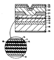
n형 GaAs기판결정(18)상에 n형 GaAs버퍼층(19), n형 Ga1-xAlxAs 크래드층(13)(X=0.45), 두께 70Å은 어도우프 GaAs웰층(11)을 5층, 10Å의 언도우프 Ga0.7AL0.3As층(15)으로 끼운 두께 20Å의 2×10¹⁸(Cm-3)의 Mg도우프를 행한 P- Ga0.7x Al0.3As 층(16)으로 형성된 배리어층 4층을 교호로 형성한 다중 양자우물활성층(20), P형 Ga1-xAlxAs크래드층(14), n형 GaAs광흡수층(21)을 MOCVD법에 의해 순차형성한다. 포토에칭공정에 의해 n형 GaAs층(21)의 중앙을 스트라이프형상으로 완전히 제거하고, P형 Ga1-xAlxAs크래드층(14)의 표면을 노출하는 폭 1∼15㎛의 홈스트라이프를 형성한다. 다음에 MOCVD법에 의해서 P형 Ga1-xAlxAs크래드층(22)(x=0.43), p형 GaAs 갭층(23)을 형성한다. 그후, P측전극(24), n측전극(25)을 형성한후, 벽개법(壁開法)에 의해, 공진기장(共振嗜長) 약 300㎛의 레이저 소자를 얻었다.an n-type n-type crystal on a GaAs substrate (18) GaAs buffer layer (19), an n-type Ga 1 -xAlxAs greater the clad layer (13) (X = 0.45) , is even undoped GaAs well layers 11 70Å thick layer 5, Barrier layer 4 formed of P-Ga0.7x
이때, P형 Ga0.55Al0.45As층(14)의 두께는 0.1∼0.5㎛일때 도파구조는 굴절율 도파형이되어 고속변조시의 가로 모우드 (tranverse mode)를 안정하게 할 수 있다.At this time, when the thickness of the P-type Ga0.
시작품으로 만든 소자는 파장 830nm에 있어서, 스레소울드 전류 10∼25mA로 실온에서 연속발진하고, 발진스텍트럼은 세로 단일 모우드를 나탄내고, 광출력은 70mW까지 킹크가 없는 안정한 가로 모우드 발진을 얻을 수 있었다. 광출력 60mW로 바이어스해서 소신호 직접변조를 행한즉, 그 변조 주파수는 15㎓(3dB다운)까지 달하는 양호한 특성을 얻을 수 있었다. 또 70℃에서 광출력 60mW의 일정한 광출력 동작시의 수명은 2000시간 경과한 후에도 현저한 열화를 볼수 없고, 신뢰성도 높은 것이 밝혀졌다. 또 다중양자 우물구조로선, 상기 이외에 Ga1-w wAlWAs웰층의 Al의 몰비 W는 0∼0.2두께 30∼150Å, 수는 2∼10, Ga-BAlBAs배리어층의 Al의 몰비 B는 0.2∼0.5(단B〉W), 양쪽다리의 언도우핑 배리어층의 두께는 2.8∼30Å, 중앙부의 P형 배리어층의 두께는 5∼50Å의 모든 결합에 있어서, 대체로 마찬가지의 변속변조 특성을 얻을 수 있었다.The prototype device has a wavelength of 830 nm, and continuously oscillates at room temperature with a threshold current of 10 to 25 mA, the oscillation spectrum exhibits a vertical single mode, and the light output is stable to no kink up to 70 mW. When small-signal direct modulation was performed by biasing at an optical output of 60 mW, a good characteristic that the modulation frequency was up to 15 Hz (3 dB down) was obtained. In addition, it was found that the life of a constant light output operation with a light output of 60 mW at 70 ° C. was not significantly deteriorated even after 2000 hours, and the reliability was high. In addition, in the multi-quantum well structure, in addition to the above, the molar ratio W of Al in the Ga 1- w wAlWAs well layer is 0 to 0.2 thickness of 30 to 150 Pa, the number is 2 to 10, and the molar ratio B of Al in the Ga aB Al B As barrier layer is 0.2 to In all combinations of 0.5 (stage B> W), the thickness of the undoped barrier layer on both legs and the thickness of the P-type barrier layer in the center and the thickness of the central portion of the P-type barrier layer were 5 to 50 µs, the same shift modulation characteristics were obtained. .
[실시예 4]Example 4
제8도를 사용해서 설명한다.Description will be made using FIG.
n형 GaAs기판(18)상에 n형 GaAlAs크래드층(13), n형 GaAlAs광안내층(26), 제7도의 실시예와 같은 다중양자 우물 활성층(20), P형 GaAlAs크래드층(14), P형 GaAs 갭층(23)을 순차 MOCVD법에 의해 형성한다. 포토에칭 공정에 의해 폭 1∼15㎛스트라이프라 남도록 P형 GaAs갭층을 제거하고, 그 스트라이프 형상의 P형 GaAs갭층(23)이외의 영역에 다중양자우물 활성층(20)을 관총할때 까지 Si를 이온주입한다.The n-type
그후 스트라이프 형상의 P형 GaAs 갭층이외의 SiO2막(28)을 피착하고, 그후 P측전극(24), n측전극(25)을 형성한 후, 벽개법에 의해, 공진기장 약 300㎛의 레이저 소자를 얻었다.After that, an SiO 2 film 28 other than a stripe-shaped P-type GaAs gap layer was deposited, and then the P-
본 실시예에 있어서도, 제7도의 실시예와 마찬가지의 특성을 얻을 수 있고, 또 활성층 구조에 괸해서도 제7도의 실시예에서 도시한 범위는 모두 적용가능하고 마찬가지의 특성을 얻을 수 있었다.Also in this embodiment, the same characteristics as in the embodiment of FIG. 7 can be obtained, and in addition to the active layer structure, all of the ranges shown in the embodiment of FIG. 7 are applicable and similar characteristics can be obtained.
[실시예 5]Example 5
제9도를 사용해서 설명한다.Description will be made using FIG.
n형 GaAs기판(18)상에 n형 GaAlAs크래드층(13), 제4도의 실시예와 마찬가지로 다중 양자우물활성층(20), P형 GaAlAs크래드층(14)을 성장한후, 포토에칭에 의해 폭 1∼5㎛의 스트라이프 형상으로 남도록 n형 GaAs기판(18)까지 이르는 에칭을 행하고, 그후 P형 GaAlAs매립층(22), n형 GaAlAs층(29)을 성장하고, Zn확산영역(30)을 형성한다. 그후 P측전극(24), n측전극(25)을 형성한 후, 벽개법에 의해 공진기장 약 300㎛의 레이저 소자를 얻었다. 본 실시예에 있어서도 양호한 고속변조 특성을 나타내고, 활성층의 주위가 모두 GaAlAs로 둘러싸여 있으므로 캐리어의 가로방향 확산이 없고 더욱 고속특성이 뛰어나며 20㎓까지의 변조를 할 수 있었다. 또 활성층 구조에 관해서도 제4도의 실시예에서 도시한 범위는, ,모두 적용 가능하고 마찬가지의 특성을 얻을 수 있었다.After the n-type
[실시예 6]Example 6
제10도를 사용해서 설명한다.Description will be made using FIG.
절연성 GaAs기판(31)상에 언도우프 GaAlAs층(32), 두께 70Å의 언도우프 GaAs웰층(11)을 3층, 두께 10Å의 언도우프 Ga0.7Al0.3As층(15)으로 끼운 두께 20Å 2×10¹⁸(cm-3)의 Se도우프를 행한 n-Ga0.7Al0.3As층(17)으로 형성된 배리어층 2층을 교호로 형성, 다시 두께 70Å의 언도우프 GaAs웰층을 2층, 두께 10Å의 언도우프 Ga0.7Al0.3As층(15)으로 끼운 두께 20Å의 2×10¹⁸(cm-3)의 Mg도우프를 행한 P-Ga0.7Al0.3As층(15)으로 형성된 배리어층 2층을 교호로 형성한 다중 양자우물활성층(20), 언도우프 GaAlAs층(32)을 형성한다. 그후, 폭 1∼5㎛의 스트라이프 형상으로 성장층을 남기고, P형 GaAlAs매립층(22), n형 GaAlAs매립층(29)을 형성한 후, P전극층(24), n전극층(25)을 형성한후, 벽개법에 의해 공진기장 약 300㎛의 레이저 소자를 얻었다. 이 레이저 소자는 활성층에 대하여, 캐리어를 가로 주입하는 구조로 되어있다. 또 다중 양자 우물활성층은, 그 배리어층에 Pn양쪽의 불순물을 공급하고 있으므로, 주입 캐리어에 대한 이득의 증가분은 더욱 커지며, 20㎓까지의 직접변조를 가능하게 하였다. 이 P, n양쪽의 불순물을 배리어층에 가진 다중 양자우물활성층을 제7도, 제8도, 제9도에 도시한 실시예에 적용한즉 마찬가지의 고속변조 특성을 얻을 수 있었다. 또 상기 각 실시예에 있어서 P형 불순물로서 Be, n형 불순물로서 Si를 적용해도 마찬가지의 결과를 얻을수 있었다.20
[실시예 7]Example 7
n형 GaAs기판(18)상에 n형 GaAlAs크래드층(13), 1×10¹⁷(cm-13)의 Mg을 도우프한 P-Ga0.8Al0.2As웰층 5층과, 2×10¹⁸(cm-3)의 Mg을 도우프한 P-Ga0.7Al0.3As배리어층 4층을 적층한 양자우물층(40)을 형성하고, 그위에 1×10¹⁷(cm-3)의 Se를 도우프한 P-Ga0.8Al0.2As웰층 4층과 1×10¹⁹(cm-3)의 Se를 도우프한 P-Ga0.7Al0.3As배리어층 4층을 적층한 양자우물층(50)을 형성하여, 양자우물활성층(20)을 형성하였다. 다시 그위에 P형 GaAlAs크래드층(14) 및 P형 GaAs갭층(23)을 순차 MOCVD법에 의해 형성하고, 그 후 실시예 4와 마찬가지로 스트라이프 구조로하고, 전극(24)(25)의 형성등을 행해서 반도체 레이저를 얻었다. 이 레이저 변조속도는 15㎓였다.n-type
[실시예 8]Example 8
n형 GaAs기판상에 n형 GaAlAs계 크래드층, 막두께 40Å의 언도우프 GaAlAs웰층 5층과 막두께 10Å의 언도우프 Ga0.7Al0.3As, 막두께 30Å의 P-Ga0.7Al0.3As 및 막두께 10Å 언도우프 Ga0.7Al0.3As를 순차 적층한 배리어층(4)을 교호로 적층한후, 그위에, 막두께 10Å의 언도우프 Ga0.7Al0.3As 층과 막두께 20Å의 P-Ga0.7Al0.3As 층으로 이루어진 배리어층과 언도우프 GaAlAs 웰층을 형성한 양자우물활성층, P형 GaAlAs계 크래드층을 MOCVD법으로 순차 형성하고, 그외는 실시예4와 마찬가지로 해서 반도체 레이저를 제작하였다. 이 반도체 레이저의 특성은 실시예 3와 마찬가지였다.An n-type GaAlAs-based cladding layer on an n-type GaAs substrate, 5 layers of an undoped GaAlAs well layer with a film thickness of 40 μs, an undoped Ga0.7Al0.3As with a film thickness of 10 μs, P-Ga0.7Al0.3As and a film thickness of 30 μs After alternately stacking a barrier layer 4 having a thickness of 10 μs of undoped Ga 0.7 Al 0.3 As sequentially laminated thereon, a 10 μm thick undoped Ga 0.7 Al 0.3 As layer and a film thickness of 20 μs of P-Ga 0.7 Al 0 were deposited. A quantum well active layer and a P-type GaAlAs-based cladding layer in which a barrier layer composed of a .3As layer and an undoped GaAlAs well layer were formed were sequentially formed by MOCVD, and the semiconductor laser was fabricated in the same manner as in Example 4. The characteristics of this semiconductor laser were the same as in Example 3.
[실시예 9]Example 9
GaAs기판상에 n형 크래드층을 형성한 후, 그위에 언도우프웰층 5층과 웰층과 접하는 1원자층을 언도우프하고, 그외의 부분을 P형으로한 배리어층 4층을 교호로 적층한 양자우물활성층을 형성하고, 그위에 P형 크래드층을 형성하고, 그외를 실시예 4와 마찬가지의 방법에 의해서 반도체 레이저를 얻었다. 이 레이저의 변조속도는 13㎓였다.After the n-type cladding layer was formed on the GaAs substrate, five layers of the undoped layer and one atomic layer in contact with the well layer were undoped thereon, and the other four layers of the P-type barrier layer were alternately stacked. A quantum well active layer was formed, a P-type cladding layer was formed thereon, and the semiconductor laser was obtained in the same manner as in Example 4. The modulation rate of this laser was 13 Hz.
또한, 상기 실시예의 반도체 레이저에 대해서, 도우핑량을 변화해서 제작한 즉 도우핑량이 5×10¹⁷(cm-3) 으로부터 본 발명의 효과가 현저히 나타났으나(제12도 참조), 도우핑량이 2×10¹⁹(cm-3) 가 되면 결정결함이 많아져서, 반도체 레이저를 얻을 수 없었다.Further, for the semiconductor laser of the above embodiment, the effect of the present invention was remarkably produced from varying the doping amount, that is, from 5 x 10 17 (cm -3 ) (see FIG. 12). When it became 2 * 10 <19> (cm <-3> ), crystal defects became large and a semiconductor laser could not be obtained.
Claims (9)
Applications Claiming Priority (4)
| Application Number | Priority Date | Filing Date | Title |
|---|---|---|---|
| JP60-164002 | 1985-07-26 | ||
| JP60164002A JPH0712103B2 (en) | 1985-07-26 | 1985-07-26 | Semiconductor laser device |
| JP60201545A JPS6262579A (en) | 1985-09-13 | 1985-09-13 | Semiconductor laser |
| JP60-201545 | 1985-09-13 |
Publications (2)
| Publication Number | Publication Date |
|---|---|
| KR870001688A KR870001688A (en) | 1987-03-17 |
| KR900000021B1 true KR900000021B1 (en) | 1990-01-18 |
Family
ID=26489276
Family Applications (1)
| Application Number | Title | Priority Date | Filing Date |
|---|---|---|---|
| KR1019860005978A Expired KR900000021B1 (en) | 1985-07-26 | 1986-07-23 | Semiconductor laser |
Country Status (1)
| Country | Link |
|---|---|
| KR (1) | KR900000021B1 (en) |
-
1986
- 1986-07-23 KR KR1019860005978A patent/KR900000021B1/en not_active Expired
Also Published As
| Publication number | Publication date |
|---|---|
| KR870001688A (en) | 1987-03-17 |
Similar Documents
| Publication | Publication Date | Title |
|---|---|---|
| EP0476689B1 (en) | Semiconductor laser and manufacturing method of the same | |
| US4881238A (en) | Semiconductor laser having quantum well active region doped with impurities | |
| JP3189791B2 (en) | Semiconductor laser | |
| JPS6254489A (en) | semiconductor light emitting device | |
| US4881235A (en) | Semiconductor laser having a multiple quantum well structure doped with impurities | |
| JPS6288389A (en) | Semiconductor light emitting element | |
| US4982408A (en) | Variable oscillation wavelength semiconduction laser device | |
| EP0293000B1 (en) | Light emitting device | |
| JP2003142774A (en) | Semiconductor laser device and method of manufacturing the same | |
| KR900000021B1 (en) | Semiconductor laser | |
| US5351254A (en) | Semiconductor laser | |
| JPS61168981A (en) | Semiconductor laser device | |
| JP2002368342A (en) | Multiplex quantum well semiconductor element | |
| JPH05211372A (en) | Manufacture of semiconductor laser | |
| JP2679974B2 (en) | Semiconductor laser device | |
| JPS6355878B2 (en) | ||
| JP3204969B2 (en) | Semiconductor laser and optical communication system | |
| JPH0712103B2 (en) | Semiconductor laser device | |
| JPH0278290A (en) | Semiconductor laser device | |
| JP2702964B2 (en) | Semiconductor laser device | |
| JP2529854B2 (en) | Infrared semiconductor laser | |
| JP3648357B2 (en) | Manufacturing method of semiconductor laser device | |
| JP2570732B2 (en) | Semiconductor laser | |
| JPH0159753B2 (en) | ||
| JPH10163561A (en) | Semiconductor laser device |
Legal Events
| Date | Code | Title | Description |
|---|---|---|---|
| A201 | Request for examination | ||
| PA0109 | Patent application |
Patent event code: PA01091R01D Comment text: Patent Application Patent event date: 19860723 |
|
| PA0201 | Request for examination |
Patent event code: PA02012R01D Patent event date: 19860723 Comment text: Request for Examination of Application |
|
| PG1501 | Laying open of application | ||
| G160 | Decision to publish patent application | ||
| PG1605 | Publication of application before grant of patent |
Comment text: Decision on Publication of Application Patent event code: PG16051S01I Patent event date: 19891125 |
|
| E701 | Decision to grant or registration of patent right | ||
| PE0701 | Decision of registration |
Patent event code: PE07011S01D Comment text: Decision to Grant Registration Patent event date: 19900413 |
|
| GRNT | Written decision to grant | ||
| PR0701 | Registration of establishment |
Comment text: Registration of Establishment Patent event date: 19900602 Patent event code: PR07011E01D |
|
| PR1002 | Payment of registration fee |
Payment date: 19900602 End annual number: 3 Start annual number: 1 |
|
| PR1001 | Payment of annual fee |
Payment date: 19930118 Start annual number: 4 End annual number: 4 |
|
| PR1001 | Payment of annual fee |
Payment date: 19940106 Start annual number: 5 End annual number: 5 |
|
| PR1001 | Payment of annual fee |
Payment date: 19950107 Start annual number: 6 End annual number: 6 |
|
| PR1001 | Payment of annual fee |
Payment date: 19960118 Start annual number: 7 End annual number: 7 |
|
| PR1001 | Payment of annual fee |
Payment date: 19970131 Start annual number: 8 End annual number: 8 |
|
| PR1001 | Payment of annual fee |
Payment date: 19971230 Start annual number: 9 End annual number: 11 |
|
| PR1001 | Payment of annual fee |
Payment date: 20010112 Start annual number: 12 End annual number: 12 |
|
| PR1001 | Payment of annual fee |
Payment date: 20020118 Start annual number: 13 End annual number: 13 |
|
| PR1001 | Payment of annual fee |
Payment date: 20030115 Start annual number: 14 End annual number: 14 |
|
| PR1001 | Payment of annual fee |
Payment date: 20040112 Start annual number: 15 End annual number: 15 |
|
| PR1001 | Payment of annual fee |
Payment date: 20050117 Start annual number: 16 End annual number: 16 |
|
| FPAY | Annual fee payment |
Payment date: 20060103 Year of fee payment: 17 |
|
| PR1001 | Payment of annual fee |
Payment date: 20060103 Start annual number: 17 End annual number: 17 |
|
| EXPY | Expiration of term | ||
| PC1801 | Expiration of term |