KR900000021B1 - 반도체 레이저 - Google Patents
반도체 레이저 Download PDFInfo
- Publication number
- KR900000021B1 KR900000021B1 KR1019860005978A KR860005978A KR900000021B1 KR 900000021 B1 KR900000021 B1 KR 900000021B1 KR 1019860005978 A KR1019860005978 A KR 1019860005978A KR 860005978 A KR860005978 A KR 860005978A KR 900000021 B1 KR900000021 B1 KR 900000021B1
- Authority
- KR
- South Korea
- Prior art keywords
- layer
- type
- well
- active layer
- quantum well
- Prior art date
- Legal status (The legal status is an assumption and is not a legal conclusion. Google has not performed a legal analysis and makes no representation as to the accuracy of the status listed.)
- Expired
Links
- 239000004065 semiconductor Substances 0.000 title claims description 48
- 230000004888 barrier function Effects 0.000 claims description 47
- 239000012535 impurity Substances 0.000 claims description 32
- 238000005253 cladding Methods 0.000 claims description 25
- 239000000758 substrate Substances 0.000 claims description 15
- 239000013078 crystal Substances 0.000 claims description 8
- 239000003574 free electron Substances 0.000 claims description 5
- 230000004907 flux Effects 0.000 claims description 3
- 238000002513 implantation Methods 0.000 claims 1
- 229910001218 Gallium arsenide Inorganic materials 0.000 description 28
- 238000000034 method Methods 0.000 description 13
- 238000002488 metal-organic chemical vapour deposition Methods 0.000 description 6
- 230000010355 oscillation Effects 0.000 description 6
- 238000009792 diffusion process Methods 0.000 description 5
- 239000000969 carrier Substances 0.000 description 4
- 238000010586 diagram Methods 0.000 description 4
- 238000002347 injection Methods 0.000 description 4
- 239000007924 injection Substances 0.000 description 4
- 238000003776 cleavage reaction Methods 0.000 description 3
- 230000003287 optical effect Effects 0.000 description 3
- 230000007017 scission Effects 0.000 description 3
- 229910004298 SiO 2 Inorganic materials 0.000 description 2
- 230000007547 defect Effects 0.000 description 2
- 230000000694 effects Effects 0.000 description 2
- 238000005530 etching Methods 0.000 description 2
- 238000001947 vapour-phase growth Methods 0.000 description 2
- 238000002425 crystallisation Methods 0.000 description 1
- 230000008025 crystallization Effects 0.000 description 1
- 230000001771 impaired effect Effects 0.000 description 1
- 238000005468 ion implantation Methods 0.000 description 1
- 230000031700 light absorption Effects 0.000 description 1
- 239000002184 metal Substances 0.000 description 1
- 229910052751 metal Inorganic materials 0.000 description 1
- 125000002524 organometallic group Chemical group 0.000 description 1
- 230000010363 phase shift Effects 0.000 description 1
- 238000001259 photo etching Methods 0.000 description 1
- 238000001228 spectrum Methods 0.000 description 1
- 230000005428 wave function Effects 0.000 description 1
Images


Classifications
-
- H—ELECTRICITY
- H01—ELECTRIC ELEMENTS
- H01S—DEVICES USING THE PROCESS OF LIGHT AMPLIFICATION BY STIMULATED EMISSION OF RADIATION [LASER] TO AMPLIFY OR GENERATE LIGHT; DEVICES USING STIMULATED EMISSION OF ELECTROMAGNETIC RADIATION IN WAVE RANGES OTHER THAN OPTICAL
- H01S3/00—Lasers, i.e. devices using stimulated emission of electromagnetic radiation in the infrared, visible or ultraviolet wave range
Landscapes
- Physics & Mathematics (AREA)
- Electromagnetism (AREA)
- Engineering & Computer Science (AREA)
- Plasma & Fusion (AREA)
- Optics & Photonics (AREA)
- Semiconductor Lasers (AREA)
Abstract
Description
Claims (9)
- 반도체 기판상에 적어도 크래드층(2), 활성층(3) 혹은 웰층(11)과 배리어층(4)을 상호로 적층해서 이루어진 다중 양자우물형 활성층(3)을 포함하는 반도체층군을 가지고, 이 활성층(3)의 두께가 결정내 자유전자의 파속의 크기보다 작은 반도체 레이저에 있어서, 이 활성층(3)에 불순물을 주입하는 것을 특징으로 하는 반도체 레이저.
- 제1항에 있어서, 불순물이 억셉터인 것을 특징으로 하는 레이저.
- 제1항에 있어서, 상기 다중 양자우물형 활성층(3)에의 불순물 주입에 있어서, 상기 웰층(활성층)(3)의 불순물 밀도보다 상기 배리어층(4)의 불순물 밀도를 크게한 것을 특징으로 하는 반도체 레이저.
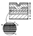
- 반도체 기판상에 형성된 복수의 반도체층 중에, 전자의 드브로이 파장 이하의 두께를 가진 웰층(11)과, 이 웰층(11)보다도 금지대폭이 넓은 배리어층(16)을 교호로 중첩시킨 다중 양자우물활성층(20)과 이 다중 양자우물활성층(20)을 끼우도록 상기 웰층(11)보다도 금지대폭이 넓은 P형(14) 및 n형크래드층(13)을 가진 반도체 레이저에 있어서, 그 다중 양자우물활성층(20)의 적층방향에 관해서 다중 양자우물활성층(20)을 형성하는 각층의 도전형이 공간적으로 다른 것을 특징으로 하는 반도체 레이저.
- 제4항에 있어서, 상기 다중 양자우물활성층중, 상기 P형 크래드층(14)으로부터 인접해서 연속하는 적어도 1조의 웰층(11)과 배리어층(15)의 도전형이 n형이며, 이 영역 이외의 다중 양자우물활성층(20)의 도전형이 P형인 것을 특징으로 하는 반도체 레이저.
- 제4항에 있어서, 상기 다중 양자우물활성층(20)중 상기 P형 크래드층(14)으로부터 인접해서 연속하는 적어도 1층의 배리어층(15)의 도전형이 n형이고, 이 영역이외의 다중 양자우물활성층(20)의 배리어층(15)의 도전형이 P형이며, 모든 웰층(11)은 언도우프인 것을 특징으로 하는 반도체 레이저.
- 제4항에 있어서, 상기 다중 양자우물층(20)중 상기 P형 크래드층(14)으로부터 인접해서 연속하는 적어도 1층의 배리어층(15)의 도전형이 n형이거나 웰층(11)과 접하는 계면으로부터 적어도 1원자층이 언도우프이고, 이 영역 이외의 다중 양자우물활성층(20)의 배리어층(15)의 도전형이 P형이거나 웰층(11)과 접하는 계면으로부터 적어도 1원자층이 언도우프이며, 모든 웰층(11)은 언도우프인 것을 특징으로 하는 반도체 레이저.
- 제4항에 있어서, 상기 배리어층(15)의 도전형이 웰층(11)과 접하는 계면으로부터 적어도 1원자층이 언도우프이고, 이 영역 이외의 배리어층(15)이 P형이며, 웰층(11)은 언도우프인 것을 특징으로 하는 반도체 레이저.
- 제4항에서 제8항까지 어느 한 항에 있어서, 상기 p형 불순물이 Be, Mg, n형 불순물이 Se, Si이며, 그 불순물 농도가 5×10¹⁷(cm-3) 이상인 것을 특징으로 하는 반도체 레이저.
Applications Claiming Priority (4)
| Application Number | Priority Date | Filing Date | Title |
|---|---|---|---|
| JP60164002A JPH0712103B2 (ja) | 1985-07-26 | 1985-07-26 | 半導体レ−ザ素子 |
| JP60-164002 | 1985-07-26 | ||
| JP60201545A JPS6262579A (ja) | 1985-09-13 | 1985-09-13 | 半導体レ−ザ装置 |
| JP60-201545 | 1985-09-13 |
Publications (2)
| Publication Number | Publication Date |
|---|---|
| KR870001688A KR870001688A (ko) | 1987-03-17 |
| KR900000021B1 true KR900000021B1 (ko) | 1990-01-18 |
Family
ID=26489276
Family Applications (1)
| Application Number | Title | Priority Date | Filing Date |
|---|---|---|---|
| KR1019860005978A Expired KR900000021B1 (ko) | 1985-07-26 | 1986-07-23 | 반도체 레이저 |
Country Status (1)
| Country | Link |
|---|---|
| KR (1) | KR900000021B1 (ko) |
-
1986
- 1986-07-23 KR KR1019860005978A patent/KR900000021B1/ko not_active Expired
Also Published As
| Publication number | Publication date |
|---|---|
| KR870001688A (ko) | 1987-03-17 |
Similar Documents
| Publication | Publication Date | Title |
|---|---|---|
| EP0476689B1 (en) | Semiconductor laser and manufacturing method of the same | |
| US4881238A (en) | Semiconductor laser having quantum well active region doped with impurities | |
| JP3189791B2 (ja) | 半導体レーザ | |
| JPS6254489A (ja) | 半導体発光素子 | |
| US4881235A (en) | Semiconductor laser having a multiple quantum well structure doped with impurities | |
| JPS6288389A (ja) | 半導体発光素子 | |
| US4982408A (en) | Variable oscillation wavelength semiconduction laser device | |
| EP0293000B1 (en) | Light emitting device | |
| JP2003142774A (ja) | 半導体レーザ装置及びその製造方法 | |
| KR900000021B1 (ko) | 반도체 레이저 | |
| US5351254A (en) | Semiconductor laser | |
| JPS61168981A (ja) | 半導体レ−ザ装置 | |
| JP2002368342A (ja) | 多重量子井戸半導体素子 | |
| JPH05211372A (ja) | 半導体レーザの製造方法 | |
| JP2679974B2 (ja) | 半導体レーザ装置 | |
| JPS6355878B2 (ko) | ||
| JP3204969B2 (ja) | 半導体レーザ及び光通信システム | |
| JPH0712103B2 (ja) | 半導体レ−ザ素子 | |
| JPH0278290A (ja) | 半導体レーザ素子 | |
| JP2702964B2 (ja) | 半導体レーザ素子 | |
| JP2529854B2 (ja) | 赤外半導体レ−ザ | |
| JP3648357B2 (ja) | 半導体レーザ素子の製造方法 | |
| JP2570732B2 (ja) | 半導体レ−ザ | |
| JPH0159753B2 (ko) | ||
| JPH10163561A (ja) | 半導体レーザ素子 |
Legal Events
| Date | Code | Title | Description |
|---|---|---|---|
| A201 | Request for examination | ||
| PA0109 | Patent application |
Patent event code: PA01091R01D Comment text: Patent Application Patent event date: 19860723 |
|
| PA0201 | Request for examination |
Patent event code: PA02012R01D Patent event date: 19860723 Comment text: Request for Examination of Application |
|
| PG1501 | Laying open of application | ||
| G160 | Decision to publish patent application | ||
| PG1605 | Publication of application before grant of patent |
Comment text: Decision on Publication of Application Patent event code: PG16051S01I Patent event date: 19891125 |
|
| E701 | Decision to grant or registration of patent right | ||
| PE0701 | Decision of registration |
Patent event code: PE07011S01D Comment text: Decision to Grant Registration Patent event date: 19900413 |
|
| GRNT | Written decision to grant | ||
| PR0701 | Registration of establishment |
Comment text: Registration of Establishment Patent event date: 19900602 Patent event code: PR07011E01D |
|
| PR1002 | Payment of registration fee |
Payment date: 19900602 End annual number: 3 Start annual number: 1 |
|
| PR1001 | Payment of annual fee |
Payment date: 19930118 Start annual number: 4 End annual number: 4 |
|
| PR1001 | Payment of annual fee |
Payment date: 19940106 Start annual number: 5 End annual number: 5 |
|
| PR1001 | Payment of annual fee |
Payment date: 19950107 Start annual number: 6 End annual number: 6 |
|
| PR1001 | Payment of annual fee |
Payment date: 19960118 Start annual number: 7 End annual number: 7 |
|
| PR1001 | Payment of annual fee |
Payment date: 19970131 Start annual number: 8 End annual number: 8 |
|
| PR1001 | Payment of annual fee |
Payment date: 19971230 Start annual number: 9 End annual number: 11 |
|
| PR1001 | Payment of annual fee |
Payment date: 20010112 Start annual number: 12 End annual number: 12 |
|
| PR1001 | Payment of annual fee |
Payment date: 20020118 Start annual number: 13 End annual number: 13 |
|
| PR1001 | Payment of annual fee |
Payment date: 20030115 Start annual number: 14 End annual number: 14 |
|
| PR1001 | Payment of annual fee |
Payment date: 20040112 Start annual number: 15 End annual number: 15 |
|
| PR1001 | Payment of annual fee |
Payment date: 20050117 Start annual number: 16 End annual number: 16 |
|
| FPAY | Annual fee payment |
Payment date: 20060103 Year of fee payment: 17 |
|
| PR1001 | Payment of annual fee |
Payment date: 20060103 Start annual number: 17 End annual number: 17 |
|
| EXPY | Expiration of term | ||
| PC1801 | Expiration of term |