KR900000052B1 - 반도체 메모리 장치 - Google Patents
반도체 메모리 장치 Download PDFInfo
- Publication number
- KR900000052B1 KR900000052B1 KR1019850005774A KR850005774A KR900000052B1 KR 900000052 B1 KR900000052 B1 KR 900000052B1 KR 1019850005774 A KR1019850005774 A KR 1019850005774A KR 850005774 A KR850005774 A KR 850005774A KR 900000052 B1 KR900000052 B1 KR 900000052B1
- Authority
- KR
- South Korea
- Prior art keywords
- data
- word
- output
- signals
- transistor
- Prior art date
- Legal status (The legal status is an assumption and is not a legal conclusion. Google has not performed a legal analysis and makes no representation as to the accuracy of the status listed.)
- Expired
Links
Images


Classifications
-
- G—PHYSICS
- G11—INFORMATION STORAGE
- G11C—STATIC STORES
- G11C11/00—Digital stores characterised by the use of particular electric or magnetic storage elements; Storage elements therefor
- G11C11/21—Digital stores characterised by the use of particular electric or magnetic storage elements; Storage elements therefor using electric elements
- G11C11/34—Digital stores characterised by the use of particular electric or magnetic storage elements; Storage elements therefor using electric elements using semiconductor devices
- G11C11/40—Digital stores characterised by the use of particular electric or magnetic storage elements; Storage elements therefor using electric elements using semiconductor devices using transistors
-
- G—PHYSICS
- G11—INFORMATION STORAGE
- G11C—STATIC STORES
- G11C7/00—Arrangements for writing information into, or reading information out from, a digital store
-
- G—PHYSICS
- G11—INFORMATION STORAGE
- G11C—STATIC STORES
- G11C11/00—Digital stores characterised by the use of particular electric or magnetic storage elements; Storage elements therefor
- G11C11/21—Digital stores characterised by the use of particular electric or magnetic storage elements; Storage elements therefor using electric elements
- G11C11/34—Digital stores characterised by the use of particular electric or magnetic storage elements; Storage elements therefor using electric elements using semiconductor devices
- G11C11/40—Digital stores characterised by the use of particular electric or magnetic storage elements; Storage elements therefor using electric elements using semiconductor devices using transistors
- G11C11/401—Digital stores characterised by the use of particular electric or magnetic storage elements; Storage elements therefor using electric elements using semiconductor devices using transistors forming cells needing refreshing or charge regeneration, i.e. dynamic cells
- G11C11/4063—Auxiliary circuits, e.g. for addressing, decoding, driving, writing, sensing or timing
- G11C11/407—Auxiliary circuits, e.g. for addressing, decoding, driving, writing, sensing or timing for memory cells of the field-effect type
- G11C11/409—Read-write [R-W] circuits
- G11C11/4094—Bit-line management or control circuits
-
- G—PHYSICS
- G11—INFORMATION STORAGE
- G11C—STATIC STORES
- G11C11/00—Digital stores characterised by the use of particular electric or magnetic storage elements; Storage elements therefor
- G11C11/21—Digital stores characterised by the use of particular electric or magnetic storage elements; Storage elements therefor using electric elements
- G11C11/34—Digital stores characterised by the use of particular electric or magnetic storage elements; Storage elements therefor using electric elements using semiconductor devices
- G11C11/40—Digital stores characterised by the use of particular electric or magnetic storage elements; Storage elements therefor using electric elements using semiconductor devices using transistors
- G11C11/401—Digital stores characterised by the use of particular electric or magnetic storage elements; Storage elements therefor using electric elements using semiconductor devices using transistors forming cells needing refreshing or charge regeneration, i.e. dynamic cells
- G11C11/4063—Auxiliary circuits, e.g. for addressing, decoding, driving, writing, sensing or timing
- G11C11/407—Auxiliary circuits, e.g. for addressing, decoding, driving, writing, sensing or timing for memory cells of the field-effect type
- G11C11/409—Read-write [R-W] circuits
- G11C11/4096—Input/output [I/O] data management or control circuits, e.g. reading or writing circuits, I/O drivers or bit-line switches
-
- G—PHYSICS
- G11—INFORMATION STORAGE
- G11C—STATIC STORES
- G11C7/00—Arrangements for writing information into, or reading information out from, a digital store
- G11C7/20—Memory cell initialisation circuits, e.g. when powering up or down, memory clear, latent image memory
Landscapes
- Engineering & Computer Science (AREA)
- Microelectronics & Electronic Packaging (AREA)
- Computer Hardware Design (AREA)
- Databases & Information Systems (AREA)
- Dram (AREA)
Abstract
Description
Claims (12)
- 다수의 비트라인쌍들, 각 비트라인쌍들을 구성하는 비트라인들에 연결되는 다수의 메모리셀들, 각각의 비트라인쌍에 대응하여 제공되며 각각 대응 비트라인쌍의 비트라인들에 연결되는 한쌍의 콤프리멘타리 신호단자(a,b)들을 각각 갖고 있는 다수의 감지 증폭기들, 선택된 비트라인쌍에 그리고 그로부터 데이타를 입력 및 출력시키기 위한 한쌍의 데이타 버스들, 각각 비트 라인쌍내의 두 비트라인들에 연결되는 각 메모리셀들의 충전상태들은 동일한 입력/출력 데이타에 대해 동일하게 되는 식으로 입력/출력 데이타를 선택적으로 반전시키기 위한 상기 쌍의 데이타 버스들에 동작하도록 연결되는 데이카 반전회로(SW), 그리고 상기 모든 메모리 셀들의 내용들이 소거되려고 할때 인가되는 소거제어신호에 반응하여 예정된 전위로 모든 비트라인들의 전위를 인출시키기 위한 클램프 회로를 포함하는 것이 특징인 반도체 메모리 장치.
- 제1항에서, 상기 각 메모리셀들은 데이타를 축적시키기 위한 캐패시터(C)와 상기 비트라인들중 하나와 상기 캐패시터간에 데이타를 전송시키기 위한 MIS트랜지스터(T)를 포함하며 그에 의해 상기 반도체 메모리장치가 다이나믹 랜돔 억세스 메모리를 구성하는 것이 특징인 반도체 메모리 장치.
- 제1항에서, 상기 출력 데이타를 제공하기 위해 상기 데이타 반전회로를 통하여 상기 데이타 버스상에 동작하도록 연결되는 출력버퍼 회로(BUF), 그리고 상기 입력 데이타를 수신하기 위해 상기 데이타 반전회로를 통하여 상기 데이타 버스쌍에 동작가능하게 연결되는 기입증폭기(WA)를 더 포함하는 것이 특징인 반도체 메모리 장치.
- 제3항에있어서, 상기 출력 버퍼회로는 콤프리멘타리의 입력신호들을 수신하기 위한 두 개의 입력(g, h)들을 갖고 있으며 상기 콤프리멘타리 입력신호들에 반응하여 상기 출력데이타가 (Dout)가 결정되며, 또한 상기 기입증폭기는 상기 입력데이타 DIN에 반응하여 결정되는 콤프리멘타리 출력신호(g,h)들을 제공하기 위한 두개의 출력들을 갖고 있는 것이 특징인 반도체 메모리 장치.
- 제4항에서, 상기 데이타 반전회로는 상기 데이타 버스들의 쌍을 상기 출력 버퍼회로의 상기 두 입력들에, 그리고 상기 기입증폭기의 두 출력들에 상기 메모리 셀들중 하나의 선택에 의해 직결 또는 횡단연결로 연결시키기 위한 스위칭 수단을 포함하는 것이 특징인 반도체 메모리 장치.
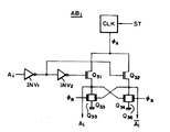
- 제5항에 있어서, 상기 각각의 비트라인쌍들중 하나와 각각 교차하는 제1군의 워드라인(WLG1)들, 상기 각 비트라인쌍들 중 다른 하나와 각각 횡단하는 제2군의 워드라인(WLG2), 그리고 어드레스 신호(A0∼A6)들을 동작가능하게 수신하여 상기 워드라인들중 하나를 선택하는 워드 디코오더(WD)를 더 포함하되, 상기 스위칭 수단은 제1, 제2, 제3 및 제4트랜지스터(Qa,Qb,Qc,Qd)들을 포함하며, 상기 제1트랜지스터는 상기 데이타 버스들중 하나와 상기 출력 버퍼회로의 상기 입력들중 하나뿐만 아니라 상기 기입증폭기의 상기 출력들 중 하나 사이에 연결되어 있으며, 상기 제2트랜지스터는 상기 데이타 버스들 중 다른 하나와 상기 출력버퍼회로의 상기 입력들 중 다른 것뿐만 아니라 상기 기입증폭기의 상기 출력들 중 다른 것 사이에 연결되어 있으며, 상기 제3트랜지스터는 상기 데이타 버스들중 상기 다른 것과 상기 출력버퍼 회로의 상기 입력들중 상기 하나뿐만 아니라 상기 기입증폭기의 상기 출력들중 상기 하나사이에 연결되어 있으며, 또한 상기 제4트랜지스터는 상기 데이타 버스들중 상기 하나와 상기 버스들의 상기 입력들중 상기 다른것뿐만 아니라 상기 기입증폭기의 상기 출력을 상기 다른 것 사이에 연결되어 있으며, 상기 제1 및 제2트랜지스터들은 상기 제1군의 워드라인들이 선택될 때 상기 어드레스 신호들에 반응하여 동시에 "온"되며 또한 상기 제3 및 제4트랜지스터들은 상기 제2군의 워드라인 들이 선택될 때 상기 어드레스 신호들에 반응하여 동시에 온되는 것이 특징인 반도체 메모리 장치.
- 제1항에서, 상기 클램프 회로는 상기 비트라인들 중 하나와 접지 사이에 각각 연결되는 다수의 클램핑(Q13, Q14, Q23, Q24)들을 포함하되, 상기 클램핑 트랜지스터들은 상기 모든 메모리 셀들의 내용들이 소거될때 상기 소거 제어신호(CLR)를 동작가능하게 수신하는 게이트 전극들을 갖는 것이 특징인 반도체 메모리 장치.
- 제2항에서, 상기 각 비트라인쌍들중 하나와 각각 교차하는 다수의 워드라인들을 더 포함하되, 각 메모리 셀내의 상기 MIS 트랜지스터는 상기 워드라인들 중 하나에 연결된 게이트 전극을 갖고 있으며 또한 상기 모든 상기 메모리 셀들의 내용들이 소거될 때 상기 MIS트랜지스터의 임계 전압보다 더 커지도록 상기 모든 워드라인들의 전위를 동시에 상승시키기 위한 워드라인 동시선택 수단을 더 포함하는 것이 특징인 반도체 메모리 장치.
- 제6항에서, 상기 워드 디코오더는 상기 모든 메모리셀의 내용들이 소거될때 상기 MIS트랜지스터의 임계전압보다 더 커지도록 상기 모든 워드라인들의 전위를 동시에 상승시키기 위한 워드라인 동시선택수단을 포함하는 것이 특징인 반도체 메모리 장치.
- 제9항에서, 상기 워드디코오더는 상기 어드레스 신호들의 콤프리멘타리 신호들을 형성하기 위한 어드레스 버퍼 유니트와 (WAB), 그리고 상기 워드라인들중 하나를 선택하도록 상기 콤프리멘타리 신호들을 선택적으로 수신하는 다수의 노아 게이트(Ni)들을 포함하되, 상기 워드라인 동시선택 수단은 상기 모든 콤프리멘타리 신호들을 저레벨로 만들어주기 위한 수단을 포함하여 그에의해 상기 노아게이트들의 모든 출력들이 고레벨이 되는 것이 특징인 반도체 메모리 장치.
- 제9항에서, 상기 워드 디코오더는 상기 어드레스 신호들의 콤프티멘타리 신호들을 형성하기 위한 어드레스 버퍼유니트와 그리고 상기 워드라인들중 하나를 선택하도록 상기 콤프리멘타리 신호들을 선택적으로 수신하는 다수의 노아게이트들을 포함하며, 상기 워드라인 동시 선택수단은 상기 노아게이트들의 모든 출력등을 고레벨로 만들어주기 위한 수단을 포함하는 것을 특징인 반도체 메모리 장치.
- 제9항에서, 상기 반도체 메모리 장치는 리세트 기간(øR)과 능동기간(øA)을 갖는 다이나믹 랜돔 억세스 메모리이며, 상기 워드 디코오더는 상기 어드레스 신호들의 콤프리멘타리 신호들을 형성하기 위한 어드레스 버퍼유니트와, 그리고 상기 워드라인들중 하나를 선택하도록 상기 콤프리멘타리 신호들을 선택적으로 수신하는 다수의 노아게이트들을 포함하되, 상기 노아게이트들 각각은 하나의 출력 트랜지스터(QT)를 갖고 있으며, 상기 워드라인 동시 선택수단은 상기 리세트 기간동안 상기 출력 트랜지스터의 각 게이트를 충전시켜서 상기 각 노아게이트들의 나머지 부분으로부터 상기 출력트랜지스터의 각 게이트를 차단시켜 주기 위한 수단을 포함하는 것이 특징인 반도체 메모리 장치.
Applications Claiming Priority (3)
| Application Number | Priority Date | Filing Date | Title |
|---|---|---|---|
| JP59-167276 | 1984-08-11 | ||
| JP59167276A JPS6148192A (ja) | 1984-08-11 | 1984-08-11 | 半導体記憶装置 |
| JP167276 | 1984-08-11 |
Publications (2)
| Publication Number | Publication Date |
|---|---|
| KR870002585A KR870002585A (ko) | 1987-03-31 |
| KR900000052B1 true KR900000052B1 (ko) | 1990-01-18 |
Family
ID=15846740
Family Applications (1)
| Application Number | Title | Priority Date | Filing Date |
|---|---|---|---|
| KR1019850005774A Expired KR900000052B1 (ko) | 1984-08-11 | 1985-08-10 | 반도체 메모리 장치 |
Country Status (5)
| Country | Link |
|---|---|
| US (1) | US4680734A (ko) |
| EP (1) | EP0172112B1 (ko) |
| JP (1) | JPS6148192A (ko) |
| KR (1) | KR900000052B1 (ko) |
| DE (1) | DE3577494D1 (ko) |
Cited By (1)
| Publication number | Priority date | Publication date | Assignee | Title |
|---|---|---|---|---|
| KR20200002122A (ko) * | 2018-06-29 | 2020-01-08 | 창원대학교 산학협력단 | 이이피롬의 데이터버스 회로 |
Families Citing this family (11)
| Publication number | Priority date | Publication date | Assignee | Title |
|---|---|---|---|---|
| JPS63177392A (ja) * | 1987-01-19 | 1988-07-21 | Toshiba Corp | 半導体記憶装置 |
| US5189639A (en) * | 1987-11-26 | 1993-02-23 | Mitsubishi Denki Kabushiki Kaisha | Semiconductor memory device having bit lines capable of partial operation |
| JP2680007B2 (ja) * | 1987-12-04 | 1997-11-19 | 株式会社日立製作所 | 半導体メモリ |
| EP0321847B1 (en) * | 1987-12-21 | 1994-06-29 | Kabushiki Kaisha Toshiba | Semiconductor memory capable of improving data rewrite speed |
| JPH0752577B2 (ja) * | 1988-01-07 | 1995-06-05 | 株式会社東芝 | 半導体メモリ |
| US5267210A (en) * | 1988-05-18 | 1993-11-30 | Sgs-Thomson Microelectronics, Inc. | SRAM with flash clear for selectable I/OS |
| JPH0770212B2 (ja) * | 1988-07-19 | 1995-07-31 | 日本電気株式会社 | 半導体メモリ回路 |
| JPH0283892A (ja) * | 1988-09-20 | 1990-03-23 | Fujitsu Ltd | 半導体記憶装置 |
| JP3191550B2 (ja) * | 1994-02-15 | 2001-07-23 | 松下電器産業株式会社 | 半導体メモリ装置 |
| GB2321123B (en) * | 1997-01-11 | 2001-01-03 | Motorola Ltd | Circuit for erasing a memory and a method thereof |
| KR100459726B1 (ko) * | 2002-10-05 | 2004-12-03 | 삼성전자주식회사 | 멀티-비트 프리페치 반도체 장치의 데이터 반전 회로 및데이터 반전 방법 |
Family Cites Families (7)
| Publication number | Priority date | Publication date | Assignee | Title |
|---|---|---|---|---|
| JPS5140830A (ko) * | 1974-10-04 | 1976-04-06 | Nippon Electric Co | |
| JPS5951072B2 (ja) * | 1979-02-26 | 1984-12-12 | 日本電気株式会社 | 半導体メモリ装置 |
| JPS6032912B2 (ja) * | 1979-09-13 | 1985-07-31 | 株式会社東芝 | Cmosセンスアンプ回路 |
| JPS58182194A (ja) * | 1982-04-20 | 1983-10-25 | Nec Corp | ダイナミツクメモリ集積回路 |
| JPS59104791A (ja) * | 1982-12-04 | 1984-06-16 | Fujitsu Ltd | 半導体記憶装置 |
| JPS59124092A (ja) * | 1982-12-29 | 1984-07-18 | Fujitsu Ltd | メモリ装置 |
| JPS60127599A (ja) * | 1983-12-14 | 1985-07-08 | Toshiba Corp | ダイナミツク型ランダムアクセスメモリ |
-
1984
- 1984-08-11 JP JP59167276A patent/JPS6148192A/ja active Pending
-
1985
- 1985-08-05 US US06/762,531 patent/US4680734A/en not_active Expired - Lifetime
- 1985-08-09 EP EP85401626A patent/EP0172112B1/en not_active Expired - Lifetime
- 1985-08-09 DE DE8585401626T patent/DE3577494D1/de not_active Expired - Lifetime
- 1985-08-10 KR KR1019850005774A patent/KR900000052B1/ko not_active Expired
Cited By (1)
| Publication number | Priority date | Publication date | Assignee | Title |
|---|---|---|---|---|
| KR20200002122A (ko) * | 2018-06-29 | 2020-01-08 | 창원대학교 산학협력단 | 이이피롬의 데이터버스 회로 |
Also Published As
| Publication number | Publication date |
|---|---|
| EP0172112A3 (en) | 1988-02-24 |
| US4680734A (en) | 1987-07-14 |
| EP0172112B1 (en) | 1990-05-02 |
| DE3577494D1 (de) | 1990-06-07 |
| KR870002585A (ko) | 1987-03-31 |
| JPS6148192A (ja) | 1986-03-08 |
| EP0172112A2 (en) | 1986-02-19 |
Similar Documents
| Publication | Publication Date | Title |
|---|---|---|
| JP2922116B2 (ja) | 半導体記憶装置 | |
| US5424975A (en) | Reference circuit for a non-volatile ferroelectric memory | |
| US5608667A (en) | Ferroelectric memory automatically generating biasing pulse for plate electrode | |
| US5406510A (en) | Non-volatile memory | |
| EP0713222A1 (en) | An integrated circuit memory device | |
| JPH0249515B2 (ko) | ||
| KR900000052B1 (ko) | 반도체 메모리 장치 | |
| JPH10106272A (ja) | 半導体記憶装置 | |
| JPH08147983A (ja) | 強誘電体メモリ装置 | |
| JPH0320836B2 (ko) | ||
| US6104635A (en) | Non-volatile memory device readable write data latch, and internal control thereof | |
| EP0448118A2 (en) | Differential cell-type EPROM incorporating stress test circuit | |
| US4602355A (en) | Memory circuit with noise preventing means for word lines | |
| KR930000898B1 (ko) | 고속으로 데이타를 소거할 수 있는 반도체 메모리 | |
| KR100341621B1 (ko) | 강유전체메모리 | |
| JPS63177392A (ja) | 半導体記憶装置 | |
| JP3717097B2 (ja) | 強誘電体メモリ | |
| EP0713223B1 (en) | Bit line sensing in a memory array | |
| EP0321847B1 (en) | Semiconductor memory capable of improving data rewrite speed | |
| JPH10162587A (ja) | 強誘電体メモリ | |
| JP3843486B2 (ja) | 不揮発性半導体記憶装置 | |
| JP3741231B2 (ja) | 不揮発性記憶装置 | |
| JP3581207B2 (ja) | 不揮発性半導体メモリ | |
| JP4119412B2 (ja) | 集積回路装置及びその試験方法 | |
| US6859377B2 (en) | Dynamic associative memory device |
Legal Events
| Date | Code | Title | Description |
|---|---|---|---|
| A201 | Request for examination | ||
| PA0109 | Patent application |
Patent event code: PA01091R01D Comment text: Patent Application Patent event date: 19850810 |
|
| PA0201 | Request for examination | ||
| PG1501 | Laying open of application | ||
| G160 | Decision to publish patent application | ||
| PG1605 | Publication of application before grant of patent |
Comment text: Decision on Publication of Application Patent event code: PG16051S01I Patent event date: 19891129 |
|
| E701 | Decision to grant or registration of patent right | ||
| PE0701 | Decision of registration |
Patent event code: PE07011S01D Comment text: Decision to Grant Registration Patent event date: 19900416 |
|
| GRNT | Written decision to grant | ||
| PR0701 | Registration of establishment |
Comment text: Registration of Establishment Patent event date: 19900713 Patent event code: PR07011E01D |
|
| PR1002 | Payment of registration fee |
Payment date: 19900713 End annual number: 3 Start annual number: 1 |
|
| PR1001 | Payment of annual fee |
Payment date: 19930115 Start annual number: 4 End annual number: 4 |
|
| PR1001 | Payment of annual fee |
Payment date: 19940113 Start annual number: 5 End annual number: 5 |
|
| PR1001 | Payment of annual fee |
Payment date: 19941227 Start annual number: 6 End annual number: 6 |
|
| PR1001 | Payment of annual fee |
Payment date: 19960115 Start annual number: 7 End annual number: 7 |
|
| PR1001 | Payment of annual fee |
Payment date: 19961230 Start annual number: 8 End annual number: 8 |
|
| PR1001 | Payment of annual fee |
Payment date: 19971223 Start annual number: 9 End annual number: 9 |
|
| PR1001 | Payment of annual fee |
Payment date: 19990112 Start annual number: 10 End annual number: 10 |
|
| PR1001 | Payment of annual fee |
Payment date: 20000107 Start annual number: 11 End annual number: 11 |
|
| PR1001 | Payment of annual fee |
Payment date: 20010111 Start annual number: 12 End annual number: 12 |
|
| PR1001 | Payment of annual fee |
Payment date: 20020110 Start annual number: 13 End annual number: 13 |
|
| PR1001 | Payment of annual fee |
Payment date: 20030109 Start annual number: 14 End annual number: 14 |
|
| PR1001 | Payment of annual fee |
Payment date: 20040109 Start annual number: 15 End annual number: 15 |
|
| FPAY | Annual fee payment |
Payment date: 20050110 Year of fee payment: 16 |
|
| PR1001 | Payment of annual fee |
Payment date: 20050110 Start annual number: 16 End annual number: 16 |
|
| EXPY | Expiration of term | ||
| PC1801 | Expiration of term |