KR900000065B1 - Read-only semiconductor memory device and manufacturing method - Google Patents
Read-only semiconductor memory device and manufacturing method Download PDFInfo
- Publication number
- KR900000065B1 KR900000065B1 KR1019860006630A KR860006630A KR900000065B1 KR 900000065 B1 KR900000065 B1 KR 900000065B1 KR 1019860006630 A KR1019860006630 A KR 1019860006630A KR 860006630 A KR860006630 A KR 860006630A KR 900000065 B1 KR900000065 B1 KR 900000065B1
- Authority
- KR
- South Korea
- Prior art keywords
- region
- semiconductor
- insulating film
- layer
- contact
- Prior art date
- Legal status (The legal status is an assumption and is not a legal conclusion. Google has not performed a legal analysis and makes no representation as to the accuracy of the status listed.)
- Expired
Links
Images


Classifications
-
- H—ELECTRICITY
- H10—SEMICONDUCTOR DEVICES; ELECTRIC SOLID-STATE DEVICES NOT OTHERWISE PROVIDED FOR
- H10B—ELECTRONIC MEMORY DEVICES
- H10B20/00—Read-only memory [ROM] devices
- H10B20/27—ROM only
- H10B20/30—ROM only having the source region and the drain region on the same level, e.g. lateral transistors
- H10B20/38—Doping programmed, e.g. mask ROM
- H10B20/383—Channel doping programmed
-
- H—ELECTRICITY
- H10—SEMICONDUCTOR DEVICES; ELECTRIC SOLID-STATE DEVICES NOT OTHERWISE PROVIDED FOR
- H10B—ELECTRONIC MEMORY DEVICES
- H10B20/00—Read-only memory [ROM] devices
-
- H—ELECTRICITY
- H10—SEMICONDUCTOR DEVICES; ELECTRIC SOLID-STATE DEVICES NOT OTHERWISE PROVIDED FOR
- H10P—GENERIC PROCESSES OR APPARATUS FOR THE MANUFACTURE OR TREATMENT OF DEVICES COVERED BY CLASS H10
- H10P30/00—Ion implantation into wafers, substrates or parts of devices
- H10P30/20—Ion implantation into wafers, substrates or parts of devices into semiconductor materials, e.g. for doping
- H10P30/22—Ion implantation into wafers, substrates or parts of devices into semiconductor materials, e.g. for doping using masks
-
- Y—GENERAL TAGGING OF NEW TECHNOLOGICAL DEVELOPMENTS; GENERAL TAGGING OF CROSS-SECTIONAL TECHNOLOGIES SPANNING OVER SEVERAL SECTIONS OF THE IPC; TECHNICAL SUBJECTS COVERED BY FORMER USPC CROSS-REFERENCE ART COLLECTIONS [XRACs] AND DIGESTS
- Y10—TECHNICAL SUBJECTS COVERED BY FORMER USPC
- Y10S—TECHNICAL SUBJECTS COVERED BY FORMER USPC CROSS-REFERENCE ART COLLECTIONS [XRACs] AND DIGESTS
- Y10S257/00—Active solid-state devices, e.g. transistors, solid-state diodes
- Y10S257/903—FET configuration adapted for use as static memory cell
Landscapes
- Semiconductor Memories (AREA)
Abstract
내용 없음.No content.
Description
제1도는 본 발명에 관한 독출전용 반도체기억장치의 제조공정을 순차적으로 나타낸 단면도.1 is a cross-sectional view sequentially showing a manufacturing process of a read-only semiconductor memory device according to the present invention.
제2도는 상기 제조공정으로 제작된 본 발명의 일실시예에 관한 ROM 메모리셀의 패턴 평면도.2 is a pattern plan view of a ROM memory cell according to an embodiment of the present invention produced by the manufacturing process.
제3도는 본 발명에 관한 독출전용 반도체기억장치의 또다른 제조공정을 순차적을 나타낸 단변도.Figure 3 is a short side view showing a sequence of another manufacturing process of the read-only semiconductor memory device according to the present invention.
제4도는 종래의 ROM 회로도.4 is a conventional ROM circuit diagram.
제5도는 제4도의 ROM 메모리셀의 패턴평면도.5 is a pattern plan view of the ROM memory cell of FIG.
제6도는 종래의 또다른 ROM 메모리셀으 패턴평면도.6 is a pattern plan view of another conventional ROM memory cell.
제7도는 제6도의 단면도이다.7 is a cross-sectional view of FIG.
* 도면의 주요부분에 대한 부호의 설명* Explanation of symbols for main parts of the drawings
11, 51 : P형 실리콘 반도체기판 12 : 게이트 산화막11, 51 P-type silicon semiconductor substrate 12: gate oxide film
13 : 제1층째의 다결정실리콘층 14 : 이온주입영역13: polysilicon layer of first layer 14: ion implantation region
15, 27 : 산화막 16A, 16B : 게이트전극 구조15, 27:
17, 18, 22, 23 : N형 반도체 영역 19 : 저온 산화막17, 18, 22, 23: N-type semiconductor region 19: low temperature oxide film
20 : 장벽 접촉구(barrier contact hole) 21 : 제2층째의 다결정실리콘층20
24 : 드레인영역 25 : 소오스영역24 drain
26 : 접촉패드(contact pad) 28, 57, 58 : 접촉구26:
29 : 알루미늄층 41 : 게이트 배선29: aluminum layer 41: gate wiring
42 : ROM 테이터선 43 : 접지선42: ROM data line 43: ground wire
44, 61 : MOS 트랜지스터44, 61: MOS transistor
45 : 데이터선(42)과 MOS 트랜지스터(44)의 드레인의 접속점45: connection point of the drain of the
46, 60 : 메모리셀영역 52 : N+형의 드레인영역46, 60: memory cell region 52: N + type drain region
54 : 게이트전극 55 : 절연막54
56 : 배선 59 : 데이터선56
본 발명의 제조시에 데이터가 기입되어 제조후에 데이터의 독출전용으로 사용되어지는 독출전요 반도체장치와 그 제조방법에 관한 것이다.BACKGROUND OF THE
일반적으로 데이터의 독출만을 수행하게 되는 독출전용 메모리(이하 ROM이라 칭함)는 웨어퍼 제조공정도중에 데이터를 기입시켜주게 됨으로서 이와 같이 제조된 ROM을 마스크 프로그램 ROM이라 칭한다.In general, a read-only memory (hereinafter referred to as a ROM) that performs only data reading, writes data during a wafer manufacturing process, and thus, the ROM thus manufactured is referred to as a mask program ROM.
그리고 이와 같은 종류의 ROM에다 데이터를 기입할 때 널리 채용되고 있는 방식으로서는 (a)접촉방식 (b)SDG방식 (c)트랜지스터의 드레숄드전압(threshold Voltage)의 차이에 의한 방식등 3종류가 있는바, 그중 상기 (a)의 방식은 데이터선과 메모리셀 트랜지스터의 드레인과의 접촉 유무에 따라 데이터의 "1"레벨 "0"레벨을 기입하도록 된 것이다.There are three widely adopted methods for writing data to this type of ROM: (a) contact method, (b) SDG method, and (c) the method due to the difference in the threshold voltage of the transistor. In the method of (a), the " 1 " level and " 0 " level of data are written in accordance with the presence or absence of contact between the data line and the drain of the memory cell transistor.
또한 상기(b)의 방식은 메모리셀 트랜지스터의 게이트영역에다 게이트 산화막을 형성시켜 준다던가 필드(field) 산화막을 형성시켜 줌에 따라 데이터"1", "0"를 기입하게 되는 것이며, (c)의 방식의 메모리셀 트랜지스터의 드레숄드전압을 높여준다던가 혹은 낮추어주게 됨에 따라 데이터를 기입하도록 된 것이다.In addition, in the method of (b), data '1' and '0' are written as the gate oxide film or the field oxide film is formed in the gate region of the memory cell transistor, and (c) The data is written as the threshold voltage of the memory cell transistor of the method increases or decreases.
그런데 상기 (a)의 접촉방법을 채용하게 되는 ROM에서는 메모리셀 1개마다 반드시 1개소의 접촉을 필요로 하기 때문에 상기 (b) 또는 (c)의 방식을 채용하게 되는 ROM에 비해 메모리셀의 면적이 커지게 된다는 단점이 따르고 있다.However, in the ROM employing the contact method of (a), one contact is required for each memory cell, and thus the area of the memory cell is larger than that of the ROM employing the method of (b) or (c). The disadvantage is that this becomes larger.
제4도는 상기 (b) 및 (c)의 방식을 이용하여 데이터를 기입하는 종래의 ROM의 회로도이고, 제5도는 이 ROM의 메모리셀 2개분의 패턴평면도로서, 도면번호 41은 메모리셀의 게이트배선, 42는 ROM 데이터선, 43은 접지선, 44는 각각 메모리셀을 구성하면서 기입데이터에 대해서 드레숄드 전압이 선택적으로 높아지게 된 MOS 트랜지스터, 45는 데이터선(42)과 각 메모리셀용 MOS 트랜지스터(44)의 드레인을 접속한 접속점을 나타낸다.FIG. 4 is a circuit diagram of a conventional ROM for writing data using the schemes (b) and (c) above. FIG. 5 is a pattern plan view of two memory cells of the ROM, and
또한 제5도에 있어서 2점 쇄선으로 둘러싸인 부분은 1개의 메모리셀영역(46)을 나타내는 바, 여기서 메모리셀의 게이트 배선(41)은 예컨대 불순물이 주입되어 저 저항화된 다결정실리콘으로 구성되어 지게되고, 데이터선(42)은 알루미늄등의 금속으로 구성되어 있다.In FIG. 5, the portion enclosed by the two-dot chain line represents one memory cell region 46, where the
상기와 같이 (b)의 SDG방식과 (c)의 트랜지스터의 드레숄드전압을 달리하는 방식을 채용하여 데이터를 기입하게 되는 ROM에서는 2개의 메모리셀마다 1개소의 접촉부위를 설치해 놓으면 되므로 상기 (a)의 접촉방식을 채용하고 있는 ROM과 비교해서 메모리셀의 크기를 적어지게 할 수가 있다.As described above, in the ROM in which data is written using the SDG method of (b) and the threshold voltage of the transistor of (c), one contact portion is provided for each two memory cells. The size of the memory cell can be made smaller than that of a ROM employing a contact method.
그리고 이런한 방식의 ROM에서는 도면상 메모리셀의 종방향크기는 접속점(45)DML 크기와 제5도 내의 치수 l로 표시되어 있는 접속점(45)과 게이트배선(41)과의 간격으로 결정되게 된다.In the ROM of this type, the longitudinal size of the memory cell in the drawing is determined by the distance between the
그런데 메모리의 점유면적을 작게하기 위해서 접속점(45)의 크기를 작아지게 하면 접촉부분의 저항이 무시할 수 없이 커지게 된다.However, if the size of the
따라서 접속점(45)의 크기를 작게하는 데에는 스스로 한계가 있게 되고, 그에 따라 메모리셀 크기의 축소화가 제한받게 된다.Therefore, there is a limit in reducing the size of the
한편 상기와 같은 구조를 탈피하여 메모리셀의 점유면적이 작고, 대용량화를 실현할 수 있는 ROM이 개발되어 있다.On the other hand, a ROM has been developed that is capable of realizing a small capacity and realizing a large capacity by deviating from the above structure.
즉 이 ROM은 실리콘반도체기판 내에 형성된 메모리셀 트랜지스터와 드레인영역에다 이 드레인영역과 같은 재질의 실리콘으로 구성된 배선을 접속시키고, 이 배선을 게이트전극 구조의 윗방향으로 연장시켜줌으로써 데이터선을 구성하게 되는 금속배선과 상기 배선과의 접촉부를 크게 취해놓고 있는 것인데, 이와 같은 ROM의 메모리셀 2개분의 패턴평면도를 제6도에, 그 a-a'선에 따른 단면도를 제7도에다 도시해 놓았다.In other words, the ROM connects a memory cell transistor formed in a silicon semiconductor substrate and a drain region to a wiring made of silicon of the same material as the drain region, and extends the wiring upwards of the gate electrode structure to form a data line. The contact portion between the metal wiring and the wiring is large. A pattern plan view of the two memory cells of the ROM is shown in FIG. 6, and a cross-sectional view along the line a-a 'is shown in FIG.
즉 제6도 및 제7도에 있어서, 도면번호 51은 P형 실리콘반도체기판, 52는 N+형의 드레인영역, 53은 N+형의 소오스영역, 54는 불순물이 주입되어 저저항화된 제1층째의 다결정실리콘으로 된 게이트전극, 55는 이 게이트 전극(54)의 위와 기판(51)의 위를 덮은 절연막, 56은 제2층째의 다결정실리콘으로된 배선, 57은 드레인영역(52)과 배선(56)사이의 접촉구, 58은 배선(56)과 알루미늄으로된 데이터선(59)사이의 접촉구를 나타낸다.6 and 7,
그리고 일점쇄선으로 둘러쌓인 부분이 1개의 메모리셀영역(60)이고, 또한 도면번호 61은 MOS 트랜지스터이다.The portion surrounded by the dashed line is one
상기와 같은 구조를 갖는 ROM에 있어서는, 실리콘반도체기판(51)내에 형성된 트랜지스터의 드레인영역(52)과 실리콘으로 구성된 배선(56)을 이른바 매립(埋立) 방식에 따라 접촉구(57)를 통해 직접접속시켜 같은 실리콘끼리 접촉시켜 줌으로서 접촉저항을 작게 할 수 있을 뿐만 아니라 접촉구(57)의 면적도 작게할 수 있다.In the ROM having the above structure, the
이런 구조로된 ROM에 의하면 알루미늄으로 된 데이터선과 메모리셀의 드레인영역을 접속시키는 SDG방식이나 이온주입 방식으로 만들어진 메모리셀에 비해 메모리셀의 점유면적이 85%정도로 되게 축소시켜 줄 수가 있게 될 뿐만 아니라, 알루미늄에 의한 데이터선(59)과 제2층재의 다결정실리콘에 의한 배선(56)사이의 접촉구(58)의 면적을 크게 취할 수가 있게되므로서, 이 부분의 접촉저항이 작아지게 되어 접촉 저항에 의한 트랜지스터 특성이 열화도 생기지 않게 되는 것이다.The ROM having such a structure can reduce the memory cell occupied area to about 85% as compared with the SDG method or the ion implantation type memory cell connecting the aluminum data line to the drain region of the memory cell. Since the area of the
그런데 제6도 및 제7도의 ROM에 있어서도, 대용량화를 위해 접촉구(57)를 형성시킬 때 제7도의 거리 d로 나타낸 부정합(misalignment) 때문에 각 칫수의 여유가 메모리셀의 한쪽방향의 크기를 대부분 점유하게 되는 것이 문제가 되고 있고, 또 마스크 배열의 정밀도를 향상시켜주는 것도 한계가 있기 때문에 이 문제를 해결하더라도 대폭적인 고밀화는 바랄 수가 없었다.However, even in the ROMs of FIGS. 6 and 7, when the
본 발명은 상기한 문제점을 해결하기 위해서 발명된 것으로서, 메모리셀의 점유면적을 축소시킬 수 있을 뿐만 아니라 대폭적인 고밀도화도 실현시킬 수 있도록 된 독출전용 반도체기억장치와 그 제조방법을 제공함에 그 목적이 있다.SUMMARY OF THE INVENTION The present invention has been invented to solve the above problems, and provides a read-only semiconductor memory device and a method for manufacturing the same, which can reduce the area occupied by a memory cell and realize a significant increase in density. There is this.
상기 목적을 달성하기 위해서 본 발명에서는 제1전도형의 절연막, 제1의 다결정실리콘층 및 제2의 절연막을 순차적으로 퇴적형성시키고, 기업정보에 따라서 상기 반도체기판내의 소정 영역에 제1전도형의 불순물을 선택적으로 이온주입하여 드레숄드전압제어를 위한 불순물 주입영역을 형성하며, 상기 제1의 절연막, 제1의 다결정실리콘층 및 제2의 절연막으로 된 3층 구조막을 선택적으로 동시에 엣칭제거하여 3층구조의 게이트전극 구조를 형성하고, 상기 게이트전극 구조를 마스크로 이용하여 상기 가판내의 역도전형의 불순물을 주입하며, 그 게이트전극 구조에 대해 자기정합적으로 또한 상호 떨어지게 하여 역전도형의 제1 및 제2의 반도체영역을 형성하고, 전면에 제3의 절연막을 퇴적형성하여, 이방성 엣칭기술에 의해 상기 게이트전극구조중 최소한 상기 제1의 반도체영역과 접한 측의 측벽에 상기 제3의 절연막을 잔존시키므로써 상기 제1의 반도체영역으로 통한 제1의 접촉구를 자기정합적으로 개구하고, 전면에 제2의 다결정실리콘층을 퇴적형성하며, 상기 제2의 다결정실리콘층에 역정도형의 불순물을 주입하여 이 다결정실리콘층을 저저항화 함으로써 상기 제1의 접촉구를 통해서 상기 제1의 반도체 영역내의 이 제1의 반도체영역보다도 깊고 불순물 농도가 높은 제3의 반도체영역을 형성시키고, 상기 저저항화된 제2의 다결정실리콘층을 선택적으로 제거하여 최소한 그일부가 상기 게이트구조의 윗방향으로 연장되게 하며, 상기 제3도 반도체영역의 표면과 접촉하는 접촉패드를 형성하고, 전면에 제4의 절연막을 퇴적형성하며, 상기 제4의 절연막에 대해 상기 접촉패드로 통하는 제2의 접촉구를 개구하고, 전면에 도전체층을 퇴적형성하며, 이것을 패터닝하여 상기 접촉패드와 접촉된 배선을 형성하도록 되어있다.In order to achieve the above object, in the present invention, the first conductive type insulating film, the first polysilicon layer, and the second insulating film are sequentially formed, and according to the company information, the first conductive type insulating film is formed in a predetermined area of the semiconductor substrate. Selectively implanting impurities to form an impurity implantation region for the threshold voltage control, and selectively etching away the three-layer structure film of the first insulating film, the first polysilicon layer, and the second insulating film Forming a gate electrode structure of a layer structure, using the gate electrode structure as a mask to inject a reverse conductivity type impurities in the substrate, and self-aligned and separated from the gate electrode structure to the first and the reverse conductivity type A second semiconductor region is formed, and a third insulating film is deposited on the entire surface, and anisotropic etching technique is used for the most of the gate electrode structures. By leaving the third insulating film on the sidewall of the side in contact with the first semiconductor region, the first contact hole through the first semiconductor region is self-aligned, and the second polycrystalline silicon is formed on the front surface. Depositing a layer, injecting an inverted impurity into the second polysilicon layer to lower the polysilicon layer, thereby reducing the first semiconductor in the first semiconductor region through the first contact hole. Forming a third semiconductor region deeper than the region and having a higher impurity concentration, selectively removing the low-resistance second polysilicon layer so that at least a portion thereof extends upwardly of the gate structure; A contact pad in contact with the surface of the semiconductor region is formed, and a fourth insulating film is deposited on the entire surface, and a second contact is brought into the contact pad with respect to the fourth insulating film. An opening and then forming a conductor layer is deposited over the entire surface, and is patterned to form a wiring it into contact with the contact pad.
이하 도면을 참조하여 본 발명의 실시예를 설명하면 다음과 같다.Hereinafter, an embodiment of the present invention will be described with reference to the accompanying drawings.
제1a도∼제1f도는 본 발명에 따른 독출전용 반도체장치의 제조방법의 일실시예의 공정순서를 나타낸 단면도로서, 이 실시예의 방법은 N채널 MOS 트랜지스터를 메모리셀로 사용한 ROM에 본 발명을 실시한 것이다.1A to 1F are cross-sectional views showing a process sequence of one embodiment of a method for manufacturing a read-only semiconductor device according to the present invention, wherein the method of the present embodiment is implemented in a ROM using an N-channel MOS transistor as a memory cell. will be.
우선 제1a도에 도시된 바와 같이 P형 실리콘 반도체기판(11)에 선택산화를 실시하여 필드절연막(도시되어 있지 않음)을 형성하여 소자를 분리한다.First, as shown in FIG. 1A, selective oxidation is performed on the P-type
특히, 필요가 있으면 상기 필드절연막을 형성시켜주기 전에 이 부분의 기판표면에다 반전방치용 불순물을 주입하여 필드절연막이 형성될 때 반전방지층을 형성시켜주는 것이 좋다.In particular, if necessary, an anti-reflective impurity may be injected into the substrate surface of this portion before the field insulating film is formed to form an anti-reflection layer when the field insulating film is formed.
다음에는 기판(11)의 노출면에다 열산화법으로 게이트 산화막(12)을 형성시켜주며, 이 게이트 절연막(12)이 형성된후 그위에다 예컨대 CVD법(화학적 기상성장법)을 써서 인(P)을 함유하고 있어 저저항화된 제1층째의 다결정실리콘층(13)을 4000∼6000Å의 두께로 퇴적형성시킨다.Next, a
이때 이 제1층째의 다결정실리콘층(13)은 처음에는 불순물이 첨가되지 않은 상태에서 형성시킨 다음 불순물로서 인(P)을 첨가하여 저저항화하는 것이 좋다.At this time, it is preferable to form the
이어 이 상태에서 전면에 도시되어 있지 않은 마스크부재를 퇴적시켜주는 한편 이 마스크부재를 PEP(사진식각)기술로 기입 데이터(ROM데이터)에 따라 패터닝하고, 이렇게 패터닝된 마스크를 이온주입용의 마스크로하여 다결정실리콘층(13) 및 게이트산화물(12)을 통해서 기판(11)에 붕소(B) 이온을 선택적으로 주입시켜 이온주입 영역(14)을 형성시킨다.Subsequently, in this state, a mask member not shown on the front surface is deposited, and the mask member is patterned according to the write data (ROM data) by PEP (photo etching) technology, and the patterned mask is used as a mask for ion implantation. The boron (B) ions are selectively implanted into the
이어 계속해서 다결정실리콘의 열산화법이나 CVD법으로 상기 다결정실리콘층(13)상의 전면에다 두께 4000Å 정도가 되는 산화막(15)을 형성시킨다.Subsequently, an
다음에는 제1b도에 도시된 바와 같이 PEP기술로 형성시켜 놓은 레지스트형상(도시되어 있지 않음)을 마스크로하여, RIE(Reactiv-ion etching; 반응성 이온엣칭)법을 써서 상기 게이트 산화막(12)과 다결정실리콘층(13) 및 산화막(15)으로 된 3층구조막을 선택적으로 제거하면서, 다결정실리콘층(13)이 게이트산화막(12) 및 산화막(15) 중간에 끼워지게 되는 3층 구조의 게이트전극 구조(16A)(16B)로 되게 형성시킨다.Next, as shown in FIG. 1B, a resist shape (not shown) formed by the PEP technique is used as a mask, and the
이어, 상기 게이트전극 구조(16A)(16B)를 마스크로하며 N형 불순물 예컨대 인(P)이나 비소(AS)등의 이온을 주입해서 기판(11)의 표면에다 N형 반도체영역(17) 및 N형 반도체영역(18)을 자가정합적으로 형성시키고, 계속해서 CVD법으로 기판전면에다 두께 5000Å 정도의 저온산화막을 퇴적시킨다.Subsequently, the
다음에는 제1c도에 도시된 바와 같이, RIE법이 갖는 이방성 엣칭작용을 이용하여 상기 저온 산화막(19)을 엣칭하되 상기 게이트전극 구조(16A)(16B) 각각의 N형반도체영역(17) 및 N형 반도체영역(18)과 접하는 방향의 양측벽상에만 저온산화막(19)을 남겨둔다.Next, as shown in FIG. 1C, the low-
또한 이와 더불어 장벽접촉구(20)를 상기 N형 반도체영역(17)상에 형성시킨다.In addition, a
그다음에는 제1d도에 도시된 바와 같이 불순물이 주입되지 않은 제2층째의 다결정실리콘층(21)을 CVD법으로 전면에 퇴적시키고, 이어 예컨대 저온의 인(P)확산등에 의해 상기 제2층째의 다결정실리콘층(21)에 불순물을 확산시켜 상기 다결정실리콘층(21)을 저저항화하고, 상기 장벽접촉구(20)를 통해서 접촉되어 있는 상기 반도체영역(17)과 상기 반도체영역(18)에다 인(P)확산을 시행하고, 이러한 영역, 즉 반도체영역(17)(18)내에 상기 반도체영역(17)(18)보다 깊이가 깊고 고농도인 N+형 반도체 영역(22)(23)을 각각 형성시킨다.Next, as shown in FIG. 1D, the
이렇게 함으로서 N형 반도칩영역(17)과 상기 N+형 반도체영역(22)으로 된 2단구조의 드레인 영역(24)과, N형 반도체영역(18)과 상기 N+형 반도체영역(23)의 2단구조로된 소오스영역(25)을 형성시켜주게 된다.In this way, a
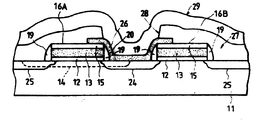
다음에는 제1e도에 도시된 바와 같이, PEP기술에 따라 형성되어진 도시되지 않은 레지스트형상을 마스크로하여 상기 제2층째의 다결정실리콘층(21)을 패터닝하고, 상기 장벽접촉구(20)를 통하여 MOS 트랜지스터의 드레인영역(24)의 표면과 접촉하는 곳에 적어도 그 일부가 상기 게이트전극 구조(16A)(16B)상에 연장되어 있는 접촉패드(26)를 형성시킨다.Next, as shown in FIG. 1E, the
다음에는 제1f도에 도시된 바와 같이, CVD법으로 전면에다 두께 10000Å정도가 되는 산화막을 퇴적시키고, 이어 다시한번 PEP법에 따라 형성되어진 도시되지 않은 레지스트 형상을 마스크로 하여 이 산화막(27)에다 접촉구(28)를 개구시켜준 다음 전공증착법등으로 알루미늄층(29)을 증착하고, 또 다시 이 알루미늄층(29)을 소정의 형태로 패터닝한다.Next, as shown in FIG. 1f, an oxide film having a thickness of about 10000 micrometers is deposited on the entire surface by CVD method, and then to the
이러한 공정으로 제조된 ROM에 있어서의 좌측의 MOS 트랜지스터에서는 드레인과 소오스영역 사이의 채널영역에 이온주입영역(14)이 형성되어져 있기 때문에 그 드레숄드 전압이 높은 값이 되게 된다.In the MOS transistor on the left side of the ROM manufactured by such a step, since the
한편 이에 비해 우측의 MOS 트랜지스터에서는 드레인, 소오스영역 사이의 채널영역에 이온주입영역이 형성되어져 있지 않게 되므로 그 드레숄드 전압은 본래 낮은 값으로 되고, 그에 따라 "1"레벨, "0"레벨의 데이터가 기입되게 된다.On the other hand, in the MOS transistor on the right side, since the ion implantation region is not formed in the channel region between the drain and the source region, the threshold voltage is inherently low, and thus the data of the '1' level and the '0' level are accordingly. Will be written.
제2도는 상기와 같은 공정으로 제작된 MOS의 메모리 개분의 패턴평면도로서, 도면에서 제1층째의 다결정실리콘층(13)을 상기 제4도의 ROM의 게이트선(41)으로 하고, 또한 패터닝된 알루미늄층(29)은 같은 ROM 데이터선(42)으로 각각 사용하므로서 일점쇄선으로 둘러진 부분이 한 개의 메모리영역으로 되며, 그에 따라 데이터선(42)으로 된 알루미늄층(29)이 접촉구로 통하여 제2층째의 다결정실리콘층(21)으로 구성된 접촉패드(26)에 접촉되며, 또한 이 접촉패드(26)는 장벽접촉구(20)(제2도에는 도시되어 있지 않음)를 통하여 드레인영역(24)에 접속되게 된다.FIG. 2 is a pattern plan view of the portion of the memory of the MOS fabricated in the above-described process, in which the
여기서 장벽접촉구(20)는 게이트전극 구조(16A)(16B)에 대히서 자기 정합적(self aline)으로 형성된다.The
따라서 제7도에 도시된 종래의 ROM의 경우에 필요로 하는 마스크 정합오차를 보상해주게 되기 때문에 치수여유(d)는 이 실시예에 장치에서 거의 필요하지 않게 된다.Therefore, since the mask matching error required in the case of the conventional ROM shown in FIG. 7 is compensated for, the dimensional margin d is hardly required in the apparatus in this embodiment.
더구나 장벽접촉구(20)는 제2도내에 도시된 소자 분리용의 필드 절연막(30)에 대해서도 장기정합적으로 형성되게 됨으로서, 이 방향에서도 정합오자를 보상해 주기 때문에 칫수여유는 필요하지 않게 된다.In addition, since the
또 상기 실시예의 ROM에서는 메모리셀의 점유면적이 제5도에 도시된 종래의 메모리셀에 대해서는 30∼40%정도를 제7도에 도시된 종래의 메모리셀에 대해서는 10∼20%정도를 각각 감소시켜 줄 수가 있어 셀크기를 축소시켜 줄 수가 있게 되며, 그에 따라 종래의 ROM과 동일한 설계기준으로 제조하여도 꽤 큰폭의 고밀도화가 달성되게 되는 것이다.In the ROM of the above embodiment, the area occupied by the memory cells is reduced by 30 to 40% for the conventional memory cell shown in FIG. 5 and about 10 to 20% for the conventional memory cell shown in FIG. Since the cell size can be reduced, the cell size can be reduced. Thus, even if manufactured according to the same design criteria as the conventional ROM, a considerably high density can be achieved.
또한 이러한 장치를 실현하기 위한 제조공정으로서는 종래의 공정으로도 충분하게 되므로 ROM의 신뢰성도 충분히 높여줄 수가 있게 되는 것이다.In addition, as a manufacturing process for realizing such a device, the conventional process is sufficient, so that the reliability of the ROM can be sufficiently increased.
또한 상기 실시예의 방법으로 제조된 장치는 드레인영역(24) 및 소오스영역(25)이 각각 교대로 자기정합의 2중 확산에 따른 2단구조로 되어 있으면서 깊이 방향으로 완만하게 경사진 영역을 갖도록 되어있다.In addition, the device manufactured by the method of the above embodiment has a
그러므로 내압이 높은 MOS 트랜지스터 및 낮은 저항값의 확산층 배선을 갖는 메모리셀을 얻을 수 있게 되는 것이다.Therefore, a memory cell having a high breakdown voltage MOS transistor and a low resistance diffusion layer wiring can be obtained.
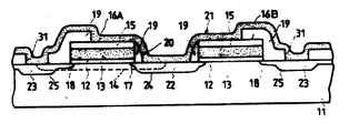
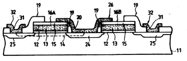
제3a도∼제3e도는 본 발명에 관한 독출전용 반도체창치의 또다른 실시예에 관한 공정순서를 나타낸 단면도로서, 본 실시예도 메모리셀로서 N채널 MOS 트랜지스터가 사용된 ROM을 제조한 경우에 대한 것이다.3A to 3E are sectional views showing a process sequence of another embodiment of the read-only semiconductor window according to the present invention. The present embodiment also shows a case in which a ROM in which an N-channel MOS transistor is used as a memory cell is manufactured. will be.
제3a도 및 제3b도까지의 공정은 제1도의 경우와 마찬가지이므로 설명을 생략한다.Since the process to FIG. 3A and FIG. 3B is the same as that of FIG. 1, description is abbreviate | omitted.
다음에는 제3c도에 도시된 바와 같이, RIE법이 갖는 이방성 엣칭작용을 이용하여 저온산화막(19)을 엣칭할 때 N형 반도체영역(17)측에만 이 저온산화막(19)이 측벽상에 남아 있도록 하는 바, 구체적으로는 N형 반도체영역(18)측을 내 엣칭성 마스크로 선택적을 덮고, 그후 RIE법으로 엣칭시킨다.Next, as shown in FIG. 3C, when etching the low
이러한 공정으로 측벽상의 저온산화막(9)은 게이트전극 구조(16A)(16B)각각의 반도체영역(17)과 접하는 쪽 측벽위에만 남아있게 되는 반면, 반도체영역(18)과 접하는 쪽에는 게이트전극 구조(16A)(16B) 각각의 윗방향까지 연장된 상태로 저온산화막(19)이 남아 있게 된다.In this process, the low-temperature oxide film 9 on the sidewalls remains only on the sidewalls in contact with the
또한 이와 더불어 장벽접촉구(20)를 상기 N형 반도체영역(17)위에 형성시킨 다음 상기 공정에서 남아 있게 된 산화막(19)에다 PEP 기술로 상기 N형 반도체 영역(17)으로 통한 접촉구(31)를 개구시켜 놓는다.In addition, a
이때 상기 접촉구(31)는 장벽접촉구(20)와 더불어 형성시켜 놓는 것이 좋다.In this case, the
이어 불순물이 주입되지 않는 제2층째의 다결정실리콘층(21)을 CVD법으로 전면에다 퇴적 형성시켜준 다음 이 다결정실리콘층(21)에 예컨대 저온의 인 확산등으로 불순물을 확산시켜 상기 다결정실리콘층(21)을 저저항화하고, 또한 상기 장벽접촉구(20) 통하여 접촉하고 있는 상기 반도체영역(17)과 상기 접촉구(31)를 통하여 접촉되여져 있는 상기 반도체영역(18)에도 인확산을 시행하며, 이러한 영역 즉 반도체영역(17)(18)내에 반도체영역(17)(18)보다도 깊고 고농도인 N+형 반도체 영역(22)(23)을 각각 형성시킨다.Subsequently, a second layer of
이렇게 N형 반도체영역(17)과 상기 N+형 반도체영역(18)으로 된 2단구조의 드레인영역(24)과, N형 반도체영역(18)과 상기 N+형 반도체영역(23)으로 된 2단구조를 갖는 소오스영역(25)이 형성되게 된다.The
다음에는 제3d도에 도시된 바와 같이, PEP기술로 형성되어진 도시되지 않은 레지스트형상을 마스크로 하여 상기 제2층째의 다결정실리콘층(21)을 패터닝함과 더불어, 상기 장벽접촉구(20)를 통하여 MOS 트랜지스터의 드레인영역(24)의 표면과 접촉시켜 주면서 적어도 그 일부분이 상기 게이트전극 구조(16A)(16B)상에 연장되어져 있는 접촉패드(26) 및 상기 접촉구(31)를 통하여 MOS 트랜지스터의 소오스영역(25)의 표면과 접촉하게 되는 접촉패드(32)를 형성시켜 준다.Next, as shown in FIG. 3D, the
이어 제3e도에 도시된 바와 같이, CVD법으로 전면에 두께 100000Å정도의 산화막(27)을 퇴적시키고, PEP법으로 형성된 도면에 도시되어 있지 않은 레지스트패턴을 마스크로 하여 이 산화막(27)에다 접촉구(28) 및 접촉구(33)를 개구시켜 준 다음, 진공층착법등으로 알루미늄층(29)을 증작시킴과 더불어 이 알루미늄층(29)을 소정의 형태로 형상화한다.Next, as shown in FIG. 3E, an
이와 같은 방법으로 제작된 ROM은 상기 접지선(43)(제4도)에 접속된 각 메모리셀의 소오스영역(25)과 같은 것을 배선으로 하지않고 알루미늄층(29)으로 구성된 배선(접지선)을 이용하여 각 소오스를 접지시켜 놓고 있는 것이다.The ROM fabricated in this manner uses a wiring (ground wire) composed of an
한편 본 발명은 상기의 실시예에 한정되지 않고 여러 가지로 변형시킬 수 있음은 물론인 바, 예를 들어 상기 실시예에서는 메모리셀용 MOS 트랜지스터의 게이트전극 및 접촉패트 각각을 다결정실리콘으로 구성시켜 놓고 있는 것에 대해서 설명하였지만, 그 이외도 예컨대 몰리브덴·실리케이트라던가 텅스텐·실리케이드등와 같은 고융점금속과 실리콘과의 혼합물 또는 고융점금속과 실리콘으로된 2층막을 이용하여 구성시켜도 좋다.In addition, the present invention is not limited to the above embodiment, and can be modified in various ways. For example, in the above embodiment, each of the gate electrode and the contact pad of the MOS transistor for a memory cell is made of polycrystalline silicon. Although the above description has been made, other than that, a high melting point metal such as molybdenum silicate, tungsten silicate or the like and a mixture of silicon or a two-layer film made of high melting point metal and silicon may be used.
즉 이러한 층이 사용될 수 있게 되는 이유로서는 확산용의 불순물을 함유할 수가 있고, 또 비교적으로 전도율이 높은 배선으로서 사용할 수가 있으며, 또한 각 공정에서의 열복사에 따라 용융될 염려가 없기 때문이다.That is, the reason why such a layer can be used is that it can contain impurities for diffusion, can be used as a relatively high conductivity wiring, and there is no fear of melting due to heat radiation in each step.
한편 상기 실시예에서는 P형 실리콘 반도체기판을 이용하고, 메모리셀이 N채널 MOS 트랜지스터로 구성된 ROM에 대해 본 발명을 실시한 경우에 대해서 설명하였지만, P형 실리콘 반도체기판을 이용한 N웰 CMOS(상보 MOS형)구조를 갖는 ROM이나 N형 실리콘 반도체기판을 이용한 P엘 CMOS 구조로된 ROM등에 대해서도 실현되어질 수 있음은 물론이다.On the other hand, in the above embodiment, the present invention has been described with respect to a ROM using a P-type silicon semiconductor substrate and a memory cell composed of N-channel MOS transistors. However, an N well CMOS (complementary MOS type) using a P-type silicon semiconductor substrate is described. Of course, the present invention can also be realized for a ROM having a structure such as a ROM and a ROM having a PEL CMOS structure using an N-type silicon semiconductor substrate.
위에서 설명한 바와 같이, 본 발명에 의하면 제1전도형의 반도체기판상에 제1의 절연막, 제1의 다결정실리콘 및 제2의 다결정실리콘막을 순차적으로 퇴적형성시키고, 기입정보에 따라서 상기 기판내의 소정영역에 제1전도형의 불순물 즉 인(P)을 선택적으로 주입하여 드레숄드전압 제어를 위한 불순물 주입영역을 형성시키며, 상기 제1의 절연막, 제1의 다결정실리콘층 및 제2의 다결정실리콘층으로 된 3층구조막을 선택적으로 동시에 엣칭제거하여 3층구조의 게이트전극 구조를 형성시키고, 상기 게이트전극 구조를 마스크로 하여 상기 기판내에다 역전도형의 불순물을 주입시키며, 이 게이트전극 구조에 대해 자기정합적으로 또는 상호 떨어지게끔 역전도형으로된 제1 및 제2반도체영역을 형성시키고, 전면에 제3의 절연막을 퇴적형성시키며, 이 방성 엣칭기술로 상기 게이트전극 구가 적어도 제1의 반도체영역과 접하는 쪽측벽상에다 상기 제3의 절연막을 잔존시켜주도록 함과 더불어 상기 제1의 반도체영역으로 통한 제1의 접촉구를 장기정합적으로 개구시켜주고, 전면에 제2의 다결정실리콘층을 퇴적형성시키며, 상기 제2의 다결정실리콘층에 역도전형불순물을 주입하여 이 다결정 실리콘층을 저저항화함과 더불어 상기 제1의 접촉구를 통해 상기 제1의 반도체영역에다 이 제1의 반도체영역에서 보다 더 깊고 불순물농도가 높은 제3의 반도체영역을 형성시킨다. 또한 상기 저저항화된 제2의 다결정실리콘층을 선택적으로 제거하여 적어도 그 일부가 상기 게이트구조의 윗방향으로 연장되게 하며, 상기 제3의 반도체영역의 표면과 접촉하는 접촉패드를 형성시키고, 전면에 제4의 절연막를 퇴적형성시키며, 상기 제4의 절연막에 대해 상기 접합패드로 통한 제2의 접촉구를 개구시켜주고, 전면에 전도체층을 퇴적형성시킨 다음 이를 패터닝하여 상기 접촉패드와 접속된 배선을 형성시켜주게 됨으로써 남은 제거분이 치수여유를 필요로 하지않기 때문에 메모리셀의 점유면적을 축소시킬 수 있을 뿐만 아니라, 대폭 고밀도화를 실현 할 수 있는 독출전용 반도체장치와 그 제조방법을 제공할 수 있게 된다.As described above, according to the present invention, a first insulating film, a first polycrystalline silicon, and a second polycrystalline silicon film are sequentially deposited on a first conductive semiconductor substrate, and a predetermined region in the substrate is formed in accordance with write information. Selectively implanting impurities of a first conductivity type, ie, phosphorus (P) into the impurity implantation region for controlling the threshold voltage, and forming the first insulating layer, the first polysilicon layer, and the second polysilicon layer Selectively etching and removing the three-layered structured film to form a three-layered gate electrode structure, and implanting reverse conductivity impurities into the substrate using the gate electrode structure as a mask, and self-aligning to the gate electrode structure. Forming the first and second semiconductor regions which are reversely conductive or separated from each other, and depositing a third insulating film on the entire surface thereof. The gate electrode sphere allows the third insulating film to remain on a side wall of the gate electrode sphere at least in contact with the first semiconductor region, and the first contact hole through the first semiconductor region is long-term consistently. Openings, depositing a second polysilicon layer on the entire surface, and injecting a reverse conductivity impurity into the second polysilicon layer to reduce the polycrystalline silicon layer and through the first contact hole. In the first semiconductor region, a third semiconductor region deeper and having a higher impurity concentration is formed than in the first semiconductor region. And selectively removing the low-resistance second polysilicon layer so that at least a portion thereof extends upwardly of the gate structure, forming a contact pad in contact with the surface of the third semiconductor region, A fourth insulating film is deposited on the second insulating film, and a second contact hole through the bonding pad is opened with respect to the fourth insulating film, and a conductor layer is deposited on the entire surface, and then patterned to form a wiring connected to the contact pad. Since the remaining removal does not require a dimensional margin, the area occupied by the memory cells can be reduced, and a read-only semiconductor device and a method of manufacturing the same can be provided which can realize a high density. do.
Claims (3)
Applications Claiming Priority (6)
| Application Number | Priority Date | Filing Date | Title |
|---|---|---|---|
| JP60177850A JPS6237961A (en) | 1985-08-13 | 1985-08-13 | Read only semiconductor memory device |
| JP177850 | 1985-08-13 | ||
| JP60-177849 | 1985-08-13 | ||
| JP60-177850 | 1985-08-13 | ||
| JP60177849A JPS6237960A (en) | 1985-08-13 | 1985-08-13 | Manufacture of read only semiconductor memory device |
| JP177849 | 1985-08-13 |
Publications (2)
| Publication Number | Publication Date |
|---|---|
| KR870002657A KR870002657A (en) | 1987-04-06 |
| KR900000065B1 true KR900000065B1 (en) | 1990-01-19 |
Family
ID=26498245
Family Applications (1)
| Application Number | Title | Priority Date | Filing Date |
|---|---|---|---|
| KR1019860006630A Expired KR900000065B1 (en) | 1985-08-13 | 1986-08-12 | Read-only semiconductor memory device and manufacturing method |
Country Status (2)
| Country | Link |
|---|---|
| US (1) | US5101262A (en) |
| KR (1) | KR900000065B1 (en) |
Families Citing this family (5)
| Publication number | Priority date | Publication date | Assignee | Title |
|---|---|---|---|---|
| JP3202784B2 (en) * | 1992-04-13 | 2001-08-27 | 三菱電機株式会社 | Mask ROM semiconductor device and method of manufacturing the same |
| KR960012252B1 (en) * | 1993-03-05 | 1996-09-18 | 삼성전자 주식회사 | Semiconductor memory device |
| KR960012259B1 (en) * | 1993-03-13 | 1996-09-18 | 삼성전자 주식회사 | Manufacturing Method of Semiconductor Device |
| US5380676A (en) * | 1994-05-23 | 1995-01-10 | United Microelectronics Corporation | Method of manufacturing a high density ROM |
| US5684313A (en) * | 1996-02-20 | 1997-11-04 | Kenney; Donald M. | Vertical precharge structure for DRAM |
Family Cites Families (26)
| Publication number | Priority date | Publication date | Assignee | Title |
|---|---|---|---|---|
| US3740835A (en) * | 1970-08-31 | 1973-06-26 | Fairchild Camera Instr Co | Method of forming semiconductor device contacts |
| US3986903A (en) * | 1974-03-13 | 1976-10-19 | Intel Corporation | Mosfet transistor and method of fabrication |
| US4169270A (en) * | 1976-12-09 | 1979-09-25 | Fairchild Camera And Instrument Corporation | Insulated-gate field-effect transistor with self-aligned contact hole to source or drain |
| JPS5552262A (en) * | 1978-10-12 | 1980-04-16 | Fujitsu Ltd | Mos semiconductor device |
| JPS5621372A (en) * | 1979-07-31 | 1981-02-27 | Fujitsu Ltd | Manufacture of semiconductor device |
| JPS5626470A (en) * | 1979-08-13 | 1981-03-14 | Hitachi Ltd | Field-effect transistor manufacturing process |
| US4376947A (en) * | 1979-09-04 | 1983-03-15 | Texas Instruments Incorporated | Electrically programmable floating gate semiconductor memory device |
| US4291391A (en) * | 1979-09-14 | 1981-09-22 | Texas Instruments Incorporated | Taper isolated random access memory array and method of operating |
| DE2947350A1 (en) * | 1979-11-23 | 1981-05-27 | Siemens AG, 1000 Berlin und 8000 München | METHOD FOR PRODUCING MNOS STORAGE TRANSISTORS WITH A VERY SHORT CHANNEL LENGTH IN SILICON GATE TECHNOLOGY |
| JPS56130970A (en) * | 1980-03-17 | 1981-10-14 | Oki Electric Ind Co Ltd | Manufacture of semiconductor device |
| US4356623A (en) * | 1980-09-15 | 1982-11-02 | Texas Instruments Incorporated | Fabrication of submicron semiconductor devices |
| US4654680A (en) * | 1980-09-24 | 1987-03-31 | Semiconductor Energy Laboratory Co., Ltd. | Sidewall gate IGFET |
| US4366613A (en) * | 1980-12-17 | 1983-01-04 | Ibm Corporation | Method of fabricating an MOS dynamic RAM with lightly doped drain |
| JPS57126147A (en) * | 1981-01-28 | 1982-08-05 | Fujitsu Ltd | Manufacture of semiconductor device |
| US4330931A (en) * | 1981-02-03 | 1982-05-25 | Intel Corporation | Process for forming metal plated regions and lines in MOS circuits |
| US4382827A (en) * | 1981-04-27 | 1983-05-10 | Ncr Corporation | Silicon nitride S/D ion implant mask in CMOS device fabrication |
| US4419809A (en) * | 1981-12-30 | 1983-12-13 | International Business Machines Corporation | Fabrication process of sub-micrometer channel length MOSFETs |
| US4419810A (en) * | 1981-12-30 | 1983-12-13 | International Business Machines Corporation | Self-aligned field effect transistor process |
| JPS5996768A (en) * | 1982-11-24 | 1984-06-04 | Mitsubishi Electric Corp | Semiconductor device |
| JPS59188974A (en) * | 1983-04-11 | 1984-10-26 | Nec Corp | Manufacture of semiconductor device |
| JPS59201461A (en) * | 1983-04-28 | 1984-11-15 | Toshiba Corp | Read only semiconductor memory device and manufacture thereof |
| US4513494A (en) * | 1983-07-19 | 1985-04-30 | American Microsystems, Incorporated | Late mask process for programming read only memories |
| JPS60116167A (en) * | 1983-11-29 | 1985-06-22 | Toshiba Corp | Semiconductor memory and manufacture thereof |
| JPS615580A (en) * | 1984-06-19 | 1986-01-11 | Toshiba Corp | Manufacture of semiconductor device |
| US4641420A (en) * | 1984-08-30 | 1987-02-10 | At&T Bell Laboratories | Metalization process for headless contact using deposited smoothing material |
| US4707457A (en) * | 1986-04-03 | 1987-11-17 | Advanced Micro Devices, Inc. | Method for making improved contact for integrated circuit structure |
-
1986
- 1986-08-12 KR KR1019860006630A patent/KR900000065B1/en not_active Expired
-
1991
- 1991-07-25 US US07/737,603 patent/US5101262A/en not_active Expired - Lifetime
Also Published As
| Publication number | Publication date |
|---|---|
| US5101262A (en) | 1992-03-31 |
| KR870002657A (en) | 1987-04-06 |
Similar Documents
| Publication | Publication Date | Title |
|---|---|---|
| US4755864A (en) | Semiconductor read only memory device with selectively present mask layer | |
| KR890004962B1 (en) | Semiconductor device and manufacturing method | |
| KR920010846B1 (en) | Method for manufacturing the semiconductor device | |
| JP3199717B2 (en) | Semiconductor device and method of manufacturing the same | |
| KR900008207B1 (en) | Semiconductor memory device | |
| US5113238A (en) | Contactless non-volatile memory array cells | |
| US5384475A (en) | Semiconductor device and method of manufacturing the same | |
| US5488242A (en) | Semiconductor memory device | |
| US4921815A (en) | Method of producing a semiconductor memory device having trench capacitors | |
| KR900000065B1 (en) | Read-only semiconductor memory device and manufacturing method | |
| KR950012744B1 (en) | Method of producing semiconductor memory device | |
| US4268847A (en) | Semiconductor device having an insulated gate type field effect transistor and method for producing the same | |
| US5055904A (en) | Semiconductor device | |
| JPH05218329A (en) | Semiconductor device and its manufacture | |
| US5227319A (en) | Method of manufacturing a semiconductor device | |
| KR900002620B1 (en) | Read-only semiconductor memory device and manufacturing method thereof | |
| JPH0795585B2 (en) | Semiconductor memory device and manufacturing method thereof | |
| EP0521690B1 (en) | Non-volatile memory and method of manufacturing the same | |
| JPS6237960A (en) | Manufacture of read only semiconductor memory device | |
| US6566197B2 (en) | Method for fabricating connection structure between segment transistor and memory cell region of flash memory device | |
| JPH05167033A (en) | Semiconductor device, semiconductor memory device, and manufacturing method thereof | |
| JP2659987B2 (en) | Semiconductor device | |
| JP2596198B2 (en) | MOS type read-only semiconductor memory device | |
| JP2760979B2 (en) | Semiconductor memory device and method of manufacturing the same | |
| JP3063203B2 (en) | Semiconductor memory and manufacturing method thereof |
Legal Events
| Date | Code | Title | Description |
|---|---|---|---|
| A201 | Request for examination | ||
| PA0109 | Patent application |
St.27 status event code: A-0-1-A10-A12-nap-PA0109 |
|
| PA0201 | Request for examination |
St.27 status event code: A-1-2-D10-D11-exm-PA0201 |
|
| R17-X000 | Change to representative recorded |
St.27 status event code: A-3-3-R10-R17-oth-X000 |
|
| PG1501 | Laying open of application |
St.27 status event code: A-1-1-Q10-Q12-nap-PG1501 |
|
| G160 | Decision to publish patent application | ||
| PG1605 | Publication of application before grant of patent |
St.27 status event code: A-2-2-Q10-Q13-nap-PG1605 |
|
| E701 | Decision to grant or registration of patent right | ||
| PE0701 | Decision of registration |
St.27 status event code: A-1-2-D10-D22-exm-PE0701 |
|
| GRNT | Written decision to grant | ||
| PR0701 | Registration of establishment |
St.27 status event code: A-2-4-F10-F11-exm-PR0701 |
|
| PR1002 | Payment of registration fee |
St.27 status event code: A-2-2-U10-U11-oth-PR1002 Fee payment year number: 1 |
|
| PR1001 | Payment of annual fee |
St.27 status event code: A-4-4-U10-U11-oth-PR1001 Fee payment year number: 4 |
|
| PR1001 | Payment of annual fee |
St.27 status event code: A-4-4-U10-U11-oth-PR1001 Fee payment year number: 5 |
|
| PR1001 | Payment of annual fee |
St.27 status event code: A-4-4-U10-U11-oth-PR1001 Fee payment year number: 6 |
|
| PR1001 | Payment of annual fee |
St.27 status event code: A-4-4-U10-U11-oth-PR1001 Fee payment year number: 7 |
|
| PR1001 | Payment of annual fee |
St.27 status event code: A-4-4-U10-U11-oth-PR1001 Fee payment year number: 8 |
|
| PR1001 | Payment of annual fee |
St.27 status event code: A-4-4-U10-U11-oth-PR1001 Fee payment year number: 9 |
|
| PR1001 | Payment of annual fee |
St.27 status event code: A-4-4-U10-U11-oth-PR1001 Fee payment year number: 10 |
|
| R18-X000 | Changes to party contact information recorded |
St.27 status event code: A-5-5-R10-R18-oth-X000 |
|
| PN2301 | Change of applicant |
St.27 status event code: A-5-5-R10-R13-asn-PN2301 St.27 status event code: A-5-5-R10-R11-asn-PN2301 |
|
| R18-X000 | Changes to party contact information recorded |
St.27 status event code: A-5-5-R10-R18-oth-X000 |
|
| R18-X000 | Changes to party contact information recorded |
St.27 status event code: A-5-5-R10-R18-oth-X000 |
|
| PR1001 | Payment of annual fee |
St.27 status event code: A-4-4-U10-U11-oth-PR1001 Fee payment year number: 11 |
|
| PR1001 | Payment of annual fee |
St.27 status event code: A-4-4-U10-U11-oth-PR1001 Fee payment year number: 12 |
|
| R18-X000 | Changes to party contact information recorded |
St.27 status event code: A-5-5-R10-R18-oth-X000 |
|
| PR1001 | Payment of annual fee |
St.27 status event code: A-4-4-U10-U11-oth-PR1001 Fee payment year number: 13 |
|
| FPAY | Annual fee payment |
Payment date: 20021231 Year of fee payment: 14 |
|
| PR1001 | Payment of annual fee |
St.27 status event code: A-4-4-U10-U11-oth-PR1001 Fee payment year number: 14 |
|
| LAPS | Lapse due to unpaid annual fee | ||
| PC1903 | Unpaid annual fee |
St.27 status event code: A-4-4-U10-U13-oth-PC1903 Not in force date: 20040120 Payment event data comment text: Termination Category : DEFAULT_OF_REGISTRATION_FEE |
|
| PC1903 | Unpaid annual fee |
St.27 status event code: N-4-6-H10-H13-oth-PC1903 Ip right cessation event data comment text: Termination Category : DEFAULT_OF_REGISTRATION_FEE Not in force date: 20040120 |
|
| P22-X000 | Classification modified |
St.27 status event code: A-4-4-P10-P22-nap-X000 |
|
| P22-X000 | Classification modified |
St.27 status event code: A-4-4-P10-P22-nap-X000 |
|
| P22-X000 | Classification modified |
St.27 status event code: A-4-4-P10-P22-nap-X000 |
|
| R18-X000 | Changes to party contact information recorded |
St.27 status event code: A-5-5-R10-R18-oth-X000 |
|
| P22-X000 | Classification modified |
St.27 status event code: A-4-4-P10-P22-nap-X000 |