KR900000065B1 - 독출전용 반도체기억장치와 그 제조방법 - Google Patents
독출전용 반도체기억장치와 그 제조방법 Download PDFInfo
- Publication number
- KR900000065B1 KR900000065B1 KR1019860006630A KR860006630A KR900000065B1 KR 900000065 B1 KR900000065 B1 KR 900000065B1 KR 1019860006630 A KR1019860006630 A KR 1019860006630A KR 860006630 A KR860006630 A KR 860006630A KR 900000065 B1 KR900000065 B1 KR 900000065B1
- Authority
- KR
- South Korea
- Prior art keywords
- region
- semiconductor
- insulating film
- layer
- contact
- Prior art date
- Legal status (The legal status is an assumption and is not a legal conclusion. Google has not performed a legal analysis and makes no representation as to the accuracy of the status listed.)
- Expired
Links
Images


Classifications
-
- H—ELECTRICITY
- H10—SEMICONDUCTOR DEVICES; ELECTRIC SOLID-STATE DEVICES NOT OTHERWISE PROVIDED FOR
- H10B—ELECTRONIC MEMORY DEVICES
- H10B20/00—Read-only memory [ROM] devices
- H10B20/27—ROM only
- H10B20/30—ROM only having the source region and the drain region on the same level, e.g. lateral transistors
- H10B20/38—Doping programmed, e.g. mask ROM
- H10B20/383—Channel doping programmed
-
- H—ELECTRICITY
- H10—SEMICONDUCTOR DEVICES; ELECTRIC SOLID-STATE DEVICES NOT OTHERWISE PROVIDED FOR
- H10B—ELECTRONIC MEMORY DEVICES
- H10B20/00—Read-only memory [ROM] devices
-
- H—ELECTRICITY
- H10—SEMICONDUCTOR DEVICES; ELECTRIC SOLID-STATE DEVICES NOT OTHERWISE PROVIDED FOR
- H10P—GENERIC PROCESSES OR APPARATUS FOR THE MANUFACTURE OR TREATMENT OF DEVICES COVERED BY CLASS H10
- H10P30/00—Ion implantation into wafers, substrates or parts of devices
- H10P30/20—Ion implantation into wafers, substrates or parts of devices into semiconductor materials, e.g. for doping
- H10P30/22—Ion implantation into wafers, substrates or parts of devices into semiconductor materials, e.g. for doping using masks
-
- Y—GENERAL TAGGING OF NEW TECHNOLOGICAL DEVELOPMENTS; GENERAL TAGGING OF CROSS-SECTIONAL TECHNOLOGIES SPANNING OVER SEVERAL SECTIONS OF THE IPC; TECHNICAL SUBJECTS COVERED BY FORMER USPC CROSS-REFERENCE ART COLLECTIONS [XRACs] AND DIGESTS
- Y10—TECHNICAL SUBJECTS COVERED BY FORMER USPC
- Y10S—TECHNICAL SUBJECTS COVERED BY FORMER USPC CROSS-REFERENCE ART COLLECTIONS [XRACs] AND DIGESTS
- Y10S257/00—Active solid-state devices, e.g. transistors, solid-state diodes
- Y10S257/903—FET configuration adapted for use as static memory cell
Landscapes
- Semiconductor Memories (AREA)
Abstract
Description
Claims (3)
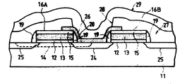
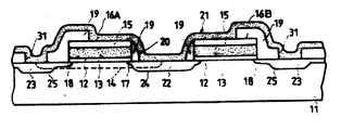
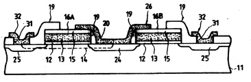
- 제1도전형의 반도체기판(11)상에다 제1의 절연막(12)과 제1의 다결정실리콘층(13) 및 제2의 절연막(15)을 순차적으로 퇴적형성시키는 공정과, 독출정보에 따라서 상기 반도체기판(11) 내의 소정영역에 제1도 전형의 불순물을 선택적으로 이온주입하여 드레숄드전압제어를 위한 불순물 주입영역(14)을 형성시키는 공정, 상기 제1의 절연막(12)과 제1의 다결정실리콘층(13) 및 제2의 절연막(15)으로 된 3층구조막을 선택적으로 동시에 엣칭제거하며 3층 구조의 게이트전극 구조(16A)(16B)를 형성시키는 공정, 상기 게이트전극 구조(16A)(16B)를 마스크로 하여 상기 반도체기판(11)내에 역전도형의 불순물을 주입하는 한편 이 게이트전극 구조(16A)(16B)에 대해 자기정합적으로 상호 떨어지게 역전도형을 갖는 제1 및 제2 반도체영역(17)(18)을 형성시켜주는 공정으로 이루어진 독출전용 반도체 장치의 제조방법에 있어서 전면에 제2의 절연막(9)의 퇴적형성시키는 공정과, 엣칭기술로 상기 게이트전극 구조중 적어도 상기 제1의 반도체영역(17)과 접촉한 측의 측벽상에 상기 제3의 절연막(19)을 남김과 더불어 상기 제1의 반도체영역(17)으로 통하는 제1의 접촉구(20)를 자기정합적으로 개구시켜 주는 공정, 전면에 제2의 다결정실리콘층(21)을 퇴적형성시키는 공정, 상기 제2의 다결정실리콘층(21)에 역도전형의 불순물을 주입하여 상기 다결정실리콘층(21)을 저저항화함과 더불어 상기 제1의 접촉구(20) 통해서 상기 제1의 반도체영역(17)내에 상기 제1의 영역(17)보다도 깊고 불순물 농도가 높은 제3의 반도체영역(22)을 형성시키는 공정, 상기 저저항화된 제2의 다결정실리콘층(21)을 선택적으로 제거하여 적어도 그 일부가 상기 게이트구조의 윗방향으로 연장되면서 상기 제3의 반도체영역의 표면과 접촉하는 접촉패드(26)를 형성시키는 공정, 전면에 제4의 절연막(27)을 퇴적형성시켜주는 공정, 상기 제4의 절연막(27)에 대해 상기 접촉패드를 통한 제2의 접촉구(28)를 개구시켜주는 공종 및 전면에 전도체층(알루미늄층)(29)을 퇴적형성시킨후, 이를 패터닝하여 상기 접촉패드와 접속된 배선(알루미늄층)(29)을 형성시켜주는 일련의 공정으로 이루어진 것을 특징으로 하는 독출전용 반도체기억장치의 제조방법.
- 제1도전형의 반도체기판(11)과, 상기 반도체기판(11)상에 형성되며 그 상하가 제1 및 제2의 절연막(12)(15)사이에 끼워진 3층구조의 게이트전극 구조(16A)(16B), 상기 게이트전극 구조(16A)(16B)에 대해 자기정합적으로 상호 떨어지게 상기 반도체기판(11)내에 형성되는 역도전형으로 된 제1 및 제2의 반도체영역(17)(18) 및, 기압정보에 따라서 상기 제1 및 제2의 반도체영역(17)(18)상호간의 체널영역에 선택적으로 형성되는 불순물 주입영역(14)을 구비한 독출전용 반도체장치에 있어서, 상기 게이트전극 구조(16A)(16B)에 적어도 한쪽의 상기 반도체영역(17)과 접하는 측벽상에 형성된 제3의 절연막(19)과, 상기 제3의 절연막(19)에 대해 자기정합적으로 상기 제1 및 제2의 반도체영역(17)(18)의 적어도 한쪽의 영역내에 형성된 제1 및 제2의 반도체영역(17)(18)보다 깊고 불순물농도가 높은 역도전형의 제3의 반도체영역(22), 적어도 그 일부가 상기 게이트구조의 윗부분으로 연장되면서 상기 제3의 전도체영역(22)의 표면과 접속되도록 형성된 제1의 도전체층(26) 및, 상기 제1의 도전체층(접촉패드)(26)과 접촉되도록 형성된 제2의 도전체층(알루미늄층)(29)을 구비하여서 된 것을 특징으로 하는 독출전형 반도체 기억장치.
- 제2항에 있어서, 도전체층(26 : 접촉패드)이 불순물을 함유한 다결정실리콘 또는 고융점금속과 실리콘의 혼합물중 어느 하나로 구성된 것을 특징으로 하는 독출전용 반도체 기억장치.
Applications Claiming Priority (6)
| Application Number | Priority Date | Filing Date | Title |
|---|---|---|---|
| JP60-177849 | 1985-08-13 | ||
| JP60-177850 | 1985-08-13 | ||
| JP60177849A JPS6237960A (ja) | 1985-08-13 | 1985-08-13 | 読み出し専用半導体記憶装置の製造方法 |
| JP177849 | 1985-08-13 | ||
| JP177850 | 1985-08-13 | ||
| JP60177850A JPS6237961A (ja) | 1985-08-13 | 1985-08-13 | 読み出し専用半導体記憶装置 |
Publications (2)
| Publication Number | Publication Date |
|---|---|
| KR870002657A KR870002657A (ko) | 1987-04-06 |
| KR900000065B1 true KR900000065B1 (ko) | 1990-01-19 |
Family
ID=26498245
Family Applications (1)
| Application Number | Title | Priority Date | Filing Date |
|---|---|---|---|
| KR1019860006630A Expired KR900000065B1 (ko) | 1985-08-13 | 1986-08-12 | 독출전용 반도체기억장치와 그 제조방법 |
Country Status (2)
| Country | Link |
|---|---|
| US (1) | US5101262A (ko) |
| KR (1) | KR900000065B1 (ko) |
Families Citing this family (5)
| Publication number | Priority date | Publication date | Assignee | Title |
|---|---|---|---|---|
| JP3202784B2 (ja) * | 1992-04-13 | 2001-08-27 | 三菱電機株式会社 | マスクrom半導体装置およびその製造方法 |
| KR960012252B1 (ko) * | 1993-03-05 | 1996-09-18 | 삼성전자 주식회사 | 반도체 메모리장치 |
| KR960012259B1 (ko) * | 1993-03-13 | 1996-09-18 | 삼성전자 주식회사 | 반도체 장치의 제조방법 |
| US5380676A (en) * | 1994-05-23 | 1995-01-10 | United Microelectronics Corporation | Method of manufacturing a high density ROM |
| US5684313A (en) * | 1996-02-20 | 1997-11-04 | Kenney; Donald M. | Vertical precharge structure for DRAM |
Family Cites Families (26)
| Publication number | Priority date | Publication date | Assignee | Title |
|---|---|---|---|---|
| US3740835A (en) * | 1970-08-31 | 1973-06-26 | Fairchild Camera Instr Co | Method of forming semiconductor device contacts |
| US3986903A (en) * | 1974-03-13 | 1976-10-19 | Intel Corporation | Mosfet transistor and method of fabrication |
| US4169270A (en) * | 1976-12-09 | 1979-09-25 | Fairchild Camera And Instrument Corporation | Insulated-gate field-effect transistor with self-aligned contact hole to source or drain |
| JPS5552262A (en) * | 1978-10-12 | 1980-04-16 | Fujitsu Ltd | Mos semiconductor device |
| JPS5621372A (en) * | 1979-07-31 | 1981-02-27 | Fujitsu Ltd | Manufacture of semiconductor device |
| JPS5626470A (en) * | 1979-08-13 | 1981-03-14 | Hitachi Ltd | Field-effect transistor manufacturing process |
| US4376947A (en) * | 1979-09-04 | 1983-03-15 | Texas Instruments Incorporated | Electrically programmable floating gate semiconductor memory device |
| US4291391A (en) * | 1979-09-14 | 1981-09-22 | Texas Instruments Incorporated | Taper isolated random access memory array and method of operating |
| DE2947350A1 (de) * | 1979-11-23 | 1981-05-27 | Siemens AG, 1000 Berlin und 8000 München | Verfahren zum herstellen von mnos-speichertransistoren mit sehr kurzer kanallaenge in silizium-gate-technologie |
| JPS56130970A (en) * | 1980-03-17 | 1981-10-14 | Oki Electric Ind Co Ltd | Manufacture of semiconductor device |
| US4356623A (en) * | 1980-09-15 | 1982-11-02 | Texas Instruments Incorporated | Fabrication of submicron semiconductor devices |
| US4654680A (en) * | 1980-09-24 | 1987-03-31 | Semiconductor Energy Laboratory Co., Ltd. | Sidewall gate IGFET |
| US4366613A (en) * | 1980-12-17 | 1983-01-04 | Ibm Corporation | Method of fabricating an MOS dynamic RAM with lightly doped drain |
| JPS57126147A (en) * | 1981-01-28 | 1982-08-05 | Fujitsu Ltd | Manufacture of semiconductor device |
| US4330931A (en) * | 1981-02-03 | 1982-05-25 | Intel Corporation | Process for forming metal plated regions and lines in MOS circuits |
| US4382827A (en) * | 1981-04-27 | 1983-05-10 | Ncr Corporation | Silicon nitride S/D ion implant mask in CMOS device fabrication |
| US4419810A (en) * | 1981-12-30 | 1983-12-13 | International Business Machines Corporation | Self-aligned field effect transistor process |
| US4419809A (en) * | 1981-12-30 | 1983-12-13 | International Business Machines Corporation | Fabrication process of sub-micrometer channel length MOSFETs |
| JPS5996768A (ja) * | 1982-11-24 | 1984-06-04 | Mitsubishi Electric Corp | 半導体装置 |
| JPS59188974A (ja) * | 1983-04-11 | 1984-10-26 | Nec Corp | 半導体装置の製造方法 |
| JPS59201461A (ja) * | 1983-04-28 | 1984-11-15 | Toshiba Corp | 読み出し専用半導体記憶装置およびその製造方法 |
| US4513494A (en) * | 1983-07-19 | 1985-04-30 | American Microsystems, Incorporated | Late mask process for programming read only memories |
| JPS60116167A (ja) * | 1983-11-29 | 1985-06-22 | Toshiba Corp | 半導体記憶装置及びその製造方法 |
| JPS615580A (ja) * | 1984-06-19 | 1986-01-11 | Toshiba Corp | 半導体装置の製造方法 |
| US4641420A (en) * | 1984-08-30 | 1987-02-10 | At&T Bell Laboratories | Metalization process for headless contact using deposited smoothing material |
| US4707457A (en) * | 1986-04-03 | 1987-11-17 | Advanced Micro Devices, Inc. | Method for making improved contact for integrated circuit structure |
-
1986
- 1986-08-12 KR KR1019860006630A patent/KR900000065B1/ko not_active Expired
-
1991
- 1991-07-25 US US07/737,603 patent/US5101262A/en not_active Expired - Lifetime
Also Published As
| Publication number | Publication date |
|---|---|
| US5101262A (en) | 1992-03-31 |
| KR870002657A (ko) | 1987-04-06 |
Similar Documents
| Publication | Publication Date | Title |
|---|---|---|
| US4755864A (en) | Semiconductor read only memory device with selectively present mask layer | |
| KR890004962B1 (ko) | 반도체장치 및 그 제조방법 | |
| KR920010846B1 (ko) | 반도체 장치의 그의 제조방법 | |
| JP3199717B2 (ja) | 半導体装置およびその製造方法 | |
| KR900008207B1 (ko) | 반도체기억장치 | |
| US5113238A (en) | Contactless non-volatile memory array cells | |
| US5384475A (en) | Semiconductor device and method of manufacturing the same | |
| US5488242A (en) | Semiconductor memory device | |
| US4921815A (en) | Method of producing a semiconductor memory device having trench capacitors | |
| KR900000065B1 (ko) | 독출전용 반도체기억장치와 그 제조방법 | |
| KR950012744B1 (ko) | 반도체 기억장치의 제조방법 | |
| US4268847A (en) | Semiconductor device having an insulated gate type field effect transistor and method for producing the same | |
| US5055904A (en) | Semiconductor device | |
| JPH05218329A (ja) | 半導体装置とその製造方法 | |
| US5227319A (en) | Method of manufacturing a semiconductor device | |
| KR900002620B1 (ko) | 독출전용 반도체기억장치 및 그 제조방법 | |
| JPH0795585B2 (ja) | 半導体記憶装置およびその製造方法 | |
| EP0521690B1 (en) | Non-volatile memory and method of manufacturing the same | |
| JPS6237960A (ja) | 読み出し専用半導体記憶装置の製造方法 | |
| US6566197B2 (en) | Method for fabricating connection structure between segment transistor and memory cell region of flash memory device | |
| JPH05167033A (ja) | 半導体装置、半導体記憶装置およびその製造方法 | |
| JP2659987B2 (ja) | 半導体装置 | |
| JP2596198B2 (ja) | Mos型読み出し専用半導体記憶装置 | |
| JP2760979B2 (ja) | 半導体記憶装置およびその製造方法 | |
| JP3063203B2 (ja) | 半導体メモリ及びその製造方法 |
Legal Events
| Date | Code | Title | Description |
|---|---|---|---|
| A201 | Request for examination | ||
| PA0109 | Patent application |
St.27 status event code: A-0-1-A10-A12-nap-PA0109 |
|
| PA0201 | Request for examination |
St.27 status event code: A-1-2-D10-D11-exm-PA0201 |
|
| R17-X000 | Change to representative recorded |
St.27 status event code: A-3-3-R10-R17-oth-X000 |
|
| PG1501 | Laying open of application |
St.27 status event code: A-1-1-Q10-Q12-nap-PG1501 |
|
| G160 | Decision to publish patent application | ||
| PG1605 | Publication of application before grant of patent |
St.27 status event code: A-2-2-Q10-Q13-nap-PG1605 |
|
| E701 | Decision to grant or registration of patent right | ||
| PE0701 | Decision of registration |
St.27 status event code: A-1-2-D10-D22-exm-PE0701 |
|
| GRNT | Written decision to grant | ||
| PR0701 | Registration of establishment |
St.27 status event code: A-2-4-F10-F11-exm-PR0701 |
|
| PR1002 | Payment of registration fee |
St.27 status event code: A-2-2-U10-U11-oth-PR1002 Fee payment year number: 1 |
|
| PR1001 | Payment of annual fee |
St.27 status event code: A-4-4-U10-U11-oth-PR1001 Fee payment year number: 4 |
|
| PR1001 | Payment of annual fee |
St.27 status event code: A-4-4-U10-U11-oth-PR1001 Fee payment year number: 5 |
|
| PR1001 | Payment of annual fee |
St.27 status event code: A-4-4-U10-U11-oth-PR1001 Fee payment year number: 6 |
|
| PR1001 | Payment of annual fee |
St.27 status event code: A-4-4-U10-U11-oth-PR1001 Fee payment year number: 7 |
|
| PR1001 | Payment of annual fee |
St.27 status event code: A-4-4-U10-U11-oth-PR1001 Fee payment year number: 8 |
|
| PR1001 | Payment of annual fee |
St.27 status event code: A-4-4-U10-U11-oth-PR1001 Fee payment year number: 9 |
|
| PR1001 | Payment of annual fee |
St.27 status event code: A-4-4-U10-U11-oth-PR1001 Fee payment year number: 10 |
|
| R18-X000 | Changes to party contact information recorded |
St.27 status event code: A-5-5-R10-R18-oth-X000 |
|
| PN2301 | Change of applicant |
St.27 status event code: A-5-5-R10-R13-asn-PN2301 St.27 status event code: A-5-5-R10-R11-asn-PN2301 |
|
| R18-X000 | Changes to party contact information recorded |
St.27 status event code: A-5-5-R10-R18-oth-X000 |
|
| R18-X000 | Changes to party contact information recorded |
St.27 status event code: A-5-5-R10-R18-oth-X000 |
|
| PR1001 | Payment of annual fee |
St.27 status event code: A-4-4-U10-U11-oth-PR1001 Fee payment year number: 11 |
|
| PR1001 | Payment of annual fee |
St.27 status event code: A-4-4-U10-U11-oth-PR1001 Fee payment year number: 12 |
|
| R18-X000 | Changes to party contact information recorded |
St.27 status event code: A-5-5-R10-R18-oth-X000 |
|
| PR1001 | Payment of annual fee |
St.27 status event code: A-4-4-U10-U11-oth-PR1001 Fee payment year number: 13 |
|
| FPAY | Annual fee payment |
Payment date: 20021231 Year of fee payment: 14 |
|
| PR1001 | Payment of annual fee |
St.27 status event code: A-4-4-U10-U11-oth-PR1001 Fee payment year number: 14 |
|
| LAPS | Lapse due to unpaid annual fee | ||
| PC1903 | Unpaid annual fee |
St.27 status event code: A-4-4-U10-U13-oth-PC1903 Not in force date: 20040120 Payment event data comment text: Termination Category : DEFAULT_OF_REGISTRATION_FEE |
|
| PC1903 | Unpaid annual fee |
St.27 status event code: N-4-6-H10-H13-oth-PC1903 Ip right cessation event data comment text: Termination Category : DEFAULT_OF_REGISTRATION_FEE Not in force date: 20040120 |
|
| P22-X000 | Classification modified |
St.27 status event code: A-4-4-P10-P22-nap-X000 |
|
| P22-X000 | Classification modified |
St.27 status event code: A-4-4-P10-P22-nap-X000 |
|
| P22-X000 | Classification modified |
St.27 status event code: A-4-4-P10-P22-nap-X000 |
|
| R18-X000 | Changes to party contact information recorded |
St.27 status event code: A-5-5-R10-R18-oth-X000 |
|
| P22-X000 | Classification modified |
St.27 status event code: A-4-4-P10-P22-nap-X000 |