RU2091908C1 - Semiconductor device - Google Patents
Semiconductor device Download PDFInfo
- Publication number
- RU2091908C1 RU2091908C1 RU94026913A RU94026913A RU2091908C1 RU 2091908 C1 RU2091908 C1 RU 2091908C1 RU 94026913 A RU94026913 A RU 94026913A RU 94026913 A RU94026913 A RU 94026913A RU 2091908 C1 RU2091908 C1 RU 2091908C1
- Authority
- RU
- Russia
- Prior art keywords
- layers
- semiconductor
- gate
- conductivity
- intermediate layer
- Prior art date
Links
- 239000004065 semiconductor Substances 0.000 title abstract description 15
- 238000009792 diffusion process Methods 0.000 abstract description 2
- 239000000126 substance Substances 0.000 abstract 1
- 239000012535 impurity Substances 0.000 description 3
- 238000004377 microelectronic Methods 0.000 description 3
- 229910004298 SiO 2 Inorganic materials 0.000 description 1
- 239000000969 carrier Substances 0.000 description 1
- 238000013461 design Methods 0.000 description 1
- 238000011161 development Methods 0.000 description 1
- 239000002019 doping agent Substances 0.000 description 1
- 238000005530 etching Methods 0.000 description 1
- 230000002452 interceptive effect Effects 0.000 description 1
- 238000000034 method Methods 0.000 description 1
- 230000003071 parasitic effect Effects 0.000 description 1
- 238000012546 transfer Methods 0.000 description 1
- 230000009466 transformation Effects 0.000 description 1
- 238000000844 transformation Methods 0.000 description 1
Images

Landscapes
- Metal-Oxide And Bipolar Metal-Oxide Semiconductor Integrated Circuits (AREA)
- Bipolar Transistors (AREA)
Abstract
Description
Изобретение относится к полупроводниковой электронике, микроэлектронике и может быть использовано в цифровых и аналоговых устройствах, в частности отказоустойчивых. The invention relates to semiconductor electronics, microelectronics and can be used in digital and analog devices, in particular fail-safe.
Один из путей создания отказоустойчивых элементов использование трансформаций функций многофункциональных полупроводниковых приборов. Реализация функций различных приборов на базе одной полупроводниковой структуры не только снижает номенклатуру элементов, но и может обеспечить повышение их отказоустойчивости, что и является целью данного изобретения. One of the ways to create fault-tolerant elements is the use of transformations of the functions of multifunctional semiconductor devices. The implementation of the functions of various devices based on one semiconductor structure not only reduces the range of elements, but can also increase their fault tolerance, which is the purpose of this invention.
Известны мощные VМДП-транзисторы с вертикальным каналом и VМДП-элементы интегральных микросхем, а также биполярные транзисторы. Каждому из этих приборов присущи свои функциональные возможности. Powerful VMDP transistors with a vertical channel and VMDP elements of integrated circuits, as well as bipolar transistors are known. Each of these devices has its own functionality.
В структуре биполярного транзистора МДП-транзистор отсутствует. В структуре VМДП-транзистора вертикальный n-p-n транзистор считают паразитным, мешающим реализации функций МДП-транзистора. Включение МДП-транзистора в качестве биполярного не предусмотрено. Выводы средних (промежуточных p-областей в VМДП-транзисторе отсутствуют, нет этих выводов и у VМДП-элементов интегральных микросхем. There is no MOS transistor in the structure of a bipolar transistor. In the structure of a VMDP transistor, a vertical n-p-n transistor is considered parasitic, interfering with the implementation of the functions of an MOS transistor. The inclusion of an MOS transistor as a bipolar is not provided. The conclusions of the middle (intermediate p-regions in the VMDP transistor are absent; these conclusions are also absent in the VMDP elements of integrated circuits.
Наиболее близким к изобретению по технической сущности может быть МДП-транзистор с вертикальным каналом ([1] рис.3.12, с.64; рис.3.13, с.65). The closest to the invention in technical essence may be a MIS transistor with a vertical channel ([1] fig. 3.12, p. 64; fig. 3.13, p. 65).
Такому транзистору присущ ряд недостатков, среди которых ограниченные функциональные возможности из-за наличия лишь одного управляющего электрода-затвора и низкая отказоустойчивость, в частности, выход прибора из строя при отказе в цепи затвора. Such a transistor has a number of drawbacks, including limited functionality due to the presence of only one gate control electrode and low fault tolerance, in particular, failure of the device in the event of a failure in the gate circuit.
Для реализации цели предлагаемого изобретения предлагается структура полупроводникового прибора, состоящая из двух горизонтальных полупроводниковых слоев одного типа проводимости и расположенного между ними тонкого слоя полупроводника другого типа проводимости. Толщина этого промежуточного слоя меньше длины диффузионного пробега носителей, концентрация легирующей (акцепторной или донорной) примеси в нем меньше, чем в соседних горизонтальных слоях. Вертикальная, формируемая анизотропным травлением канавка разделяет два слоя на отдельные области. На поверхности канавки сформированы слои диэлектрика и затвора. Каждая область структуры и затвор имеют внешние омические контакты (электроды). To achieve the objective of the invention, a semiconductor device structure is proposed consisting of two horizontal semiconductor layers of one type of conductivity and a thin layer of a semiconductor of another type of conductivity located between them. The thickness of this intermediate layer is less than the diffusion path of the carriers, the concentration of the dopant (acceptor or donor) impurity in it is less than in neighboring horizontal layers. A vertical groove formed by anisotropic etching divides the two layers into separate regions. Dielectric and gate layers are formed on the surface of the groove. Each structure region and gate have external ohmic contacts (electrodes).
Благодаря вышеуказанному реализуются новые свойства прибора возможность его работы не только в качестве МДП-транзистора, но и в качестве биполярного транзистора, а также в качестве нового отказоустойчивого элемента с двумя и более управляющими электродами. Thanks to the above, new properties of the device are realized.The possibility of its operation not only as an MOS transistor, but also as a bipolar transistor, as well as as a new fail-safe element with two or more control electrodes.
Снижение концентрации примеси в промежуточном слое (1012-1014 см-3) и его малая толщина (0,4 0,6) мкм обеспечивают хорошие частотные свойства транзисторов, высокий коэффициент передачи тока биполярного транзистора и увеличение токов МДП-транзистора.The decrease in the concentration of the impurity in the intermediate layer (10 12 -10 14 cm -3 ) and its small thickness (0.4 0.6) μm provide good frequency properties of the transistors, a high current transfer coefficient of the bipolar transistor and an increase in the currents of the MOS transistor.
За счет уменьшения толщины промежуточного слоя и концентрации примесей в нем получены новые свойства структуры, результатом чего является необходимость изменения конструкции прибора обеспечение дополнительных внешних электродов от областей промежуточного слоя для их использования в качестве управляющих. By reducing the thickness of the intermediate layer and the concentration of impurities in it, new structure properties are obtained, the result of which is the need to change the design of the device providing additional external electrodes from the regions of the intermediate layer for their use as control.
Вариант структуры предлагаемого полупроводникового прибора приведен на фиг. 1. Данная структура содержит области n+-проводимости 1', 3', 5' и n-проводимости 7', расположенные между ними области промежуточного p-слоя 2', 6', вертикальную канавку, стенки которой несут слои диэлектрика SiO2 и затвора 4'. Электроды 1-6 выводы областей 1'-6' соответственно.A variant of the structure of the proposed semiconductor device is shown in FIG. 1. This structure contains the regions of n + conductivity 1 ', 3', 5 'and n-conductivity 7', the regions of the intermediate p-layer 2 ', 6' located between them, a vertical groove, the walls of which carry layers of a dielectric SiO 2 and shutter 4 '. The electrodes 1-6 leads the areas 1'-6 ', respectively.
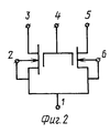
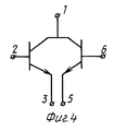
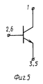
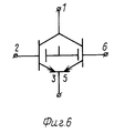
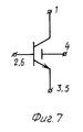
Варианты коммутации выводов прибора при работе его в качестве МДП-транзисторов, биполярных транзисторов, в качестве приборов с двумя и тремя управляющими электродами приведены на фиг. 2-7 соответственно. Options for switching the terminals of the device when it is used as MIS transistors, bipolar transistors, as devices with two and three control electrodes are shown in FIG. 2-7 respectively.
Технический результат изобретения состоит в объединении функций биполярного транзистора и МДП-транзистора в одной полупроводниковой структуре, возможности использовать ее в качестве полупроводникового прибора с двумя и более управляющими электродами и соответственно расширенными возможностями функционирования и отказоустойчивости. The technical result of the invention consists in combining the functions of a bipolar transistor and an MOS transistor in one semiconductor structure, the possibility of using it as a semiconductor device with two or more control electrodes and, accordingly, expanded functionality and fault tolerance.
Например, при отказе в цепи затвора коммутация входного сигнала в цепь области промежуточного слоя базы биполярного транзистора позволяет сохранить работоспособность схемы при незначительном изменении сигнала на выходе. For example, in the event of a failure in the gate circuit, switching the input signal into the circuit of the region of the intermediate layer of the base of the bipolar transistor allows you to maintain the operability of the circuit with a slight change in the output signal.
Разработка отказоустойчивых устройств на основе предлагаемого устройства чрезвычайно актуальна для применения в аппаратуре железнодорожного транспорта, авиации и др. The development of fault-tolerant devices based on the proposed device is extremely relevant for use in the equipment of railway transport, aviation, etc.
Применение изобретения в микроэлектронике для би-МОП интегральных микросхем позволяет реализовать их биполярные и МДП-элементы на базе одной и той же полупроводниковой структуры при едином технологическом процессе. The application of the invention in microelectronics for bi-MOS integrated circuits makes it possible to realize their bipolar and MIS elements on the basis of the same semiconductor structure with a single technological process.
Источники информации. Sources of information.
1. Окснер Э. С. Мощные полевые транзисторы и их применение. М. Радио и связь, 1985, с. 64-65. 1. Oxner E. S. Powerful field-effect transistors and their application. M. Radio and Communications, 1985, p. 64-65.
2. Полупроводниковые приборы. Транзисторы средней и большой мощности. Справочник под ред. А.В. Голомедова. М. Радио и связь, 1989. 2. Semiconductor devices. Medium and high power transistors. Handbook Ed. A.V. Golomedova. M. Radio and Communications, 1989.
3. Аваев Н.А. и др. Основы микроэлектроники. М. Радио и связь, 1991, с. 92-93. 3. Avaev N.A. et al. Fundamentals of Microelectronics. M. Radio and Communications, 1991, p. 92-93.
4. Либерман Ф. Я. Электроника на железнодорожном транспорте. М. Транспорт, 1987, с.76-85, 181. 4. Liberman F. Ya. Electronics in railway transport. M. Transport, 1987, pp. 76-85, 181.
Claims (1)
Priority Applications (1)
| Application Number | Priority Date | Filing Date | Title |
|---|---|---|---|
| RU94026913A RU2091908C1 (en) | 1994-07-15 | 1994-07-15 | Semiconductor device |
Applications Claiming Priority (1)
| Application Number | Priority Date | Filing Date | Title |
|---|---|---|---|
| RU94026913A RU2091908C1 (en) | 1994-07-15 | 1994-07-15 | Semiconductor device |
Publications (2)
| Publication Number | Publication Date |
|---|---|
| RU94026913A RU94026913A (en) | 1996-07-27 |
| RU2091908C1 true RU2091908C1 (en) | 1997-09-27 |
Family
ID=20158586
Family Applications (1)
| Application Number | Title | Priority Date | Filing Date |
|---|---|---|---|
| RU94026913A RU2091908C1 (en) | 1994-07-15 | 1994-07-15 | Semiconductor device |
Country Status (1)
| Country | Link |
|---|---|
| RU (1) | RU2091908C1 (en) |
Cited By (2)
| Publication number | Priority date | Publication date | Assignee | Title |
|---|---|---|---|---|
| RU2189089C2 (en) * | 2000-08-24 | 2002-09-10 | Государственное унитарное предприятие "Научно-производственное предприятие "Пульсар" | High-power dmos-transistor manufacturing process |
| RU2192691C2 (en) * | 1997-01-09 | 2002-11-10 | Московский государственный университет путей сообщения | Complementary semiconductor device |
-
1994
- 1994-07-15 RU RU94026913A patent/RU2091908C1/en active
Non-Patent Citations (1)
| Title |
|---|
| Oкспер Э.С. Мощные полевые транзисторы и их применение. - М.: Радио и связь, 1985, с.64 и 65. * |
Cited By (2)
| Publication number | Priority date | Publication date | Assignee | Title |
|---|---|---|---|---|
| RU2192691C2 (en) * | 1997-01-09 | 2002-11-10 | Московский государственный университет путей сообщения | Complementary semiconductor device |
| RU2189089C2 (en) * | 2000-08-24 | 2002-09-10 | Государственное унитарное предприятие "Научно-производственное предприятие "Пульсар" | High-power dmos-transistor manufacturing process |
Also Published As
| Publication number | Publication date |
|---|---|
| RU94026913A (en) | 1996-07-27 |
Similar Documents
| Publication | Publication Date | Title |
|---|---|---|
| US6288424B1 (en) | Semiconductor device having LDMOS transistors and a screening layer | |
| KR930003557B1 (en) | Transmission gate | |
| EP1040521B1 (en) | Method of operating a silicon oxide insulator (soi) semiconductor having selectively linked body | |
| US3339128A (en) | Insulated offset gate field effect transistor | |
| KR890004472B1 (en) | CMOS integrated circuit | |
| GB1561903A (en) | Fild effect transistors | |
| KR20000029578A (en) | Semiconkuctor component for high voltage | |
| CA1160760A (en) | Field-effect capacitance | |
| US4712124A (en) | Complementary lateral insulated gate rectifiers with matched "on" resistances | |
| US3488564A (en) | Planar epitaxial resistors | |
| HK79493A (en) | Integrated circuit of the complementary technique having a substrate bias generator | |
| HK68594A (en) | Integrated circuit having latch-up protection circuit fabricated by complementary MOS technology | |
| EP0247660B1 (en) | Semiconductor device comprising a bipolar transistor and field-effect transistors | |
| US7816212B2 (en) | Method of high voltage operation of a field effect transistor | |
| JPH0846059A (en) | Integrated circuit chip | |
| US3585463A (en) | Complementary enhancement-type mos transistors | |
| US6525392B1 (en) | Semiconductor power device with insulated circuit | |
| US4063273A (en) | Fundamental logic circuit | |
| EP0708486B1 (en) | Semiconductor field effect transistor with large substrate contact region | |
| CA1047646A (en) | Complementary storage element | |
| US6995453B2 (en) | High voltage integrated circuit including bipolar transistor within high voltage island area | |
| US5309009A (en) | Integrated electrically adjustable analog transistor device | |
| JPH02226808A (en) | Power mosfet with overcurrent protecting function | |
| US4761679A (en) | Complementary silicon-on-insulator lateral insulated gate rectifiers | |
| US6441446B1 (en) | Device with integrated bipolar and MOSFET transistors in an emitter switching configuration |