TW202000941A - Aluminum alloy film, manufacturing method for the same, and thin film transistor - Google Patents
Aluminum alloy film, manufacturing method for the same, and thin film transistor Download PDFInfo
- Publication number
- TW202000941A TW202000941A TW108120573A TW108120573A TW202000941A TW 202000941 A TW202000941 A TW 202000941A TW 108120573 A TW108120573 A TW 108120573A TW 108120573 A TW108120573 A TW 108120573A TW 202000941 A TW202000941 A TW 202000941A
- Authority
- TW
- Taiwan
- Prior art keywords
- atomic
- alloy film
- additive element
- aluminum alloy
- less
- Prior art date
Links
Images


Classifications
-
- C—CHEMISTRY; METALLURGY
- C23—COATING METALLIC MATERIAL; COATING MATERIAL WITH METALLIC MATERIAL; CHEMICAL SURFACE TREATMENT; DIFFUSION TREATMENT OF METALLIC MATERIAL; COATING BY VACUUM EVAPORATION, BY SPUTTERING, BY ION IMPLANTATION OR BY CHEMICAL VAPOUR DEPOSITION, IN GENERAL; INHIBITING CORROSION OF METALLIC MATERIAL OR INCRUSTATION IN GENERAL
- C23C—COATING METALLIC MATERIAL; COATING MATERIAL WITH METALLIC MATERIAL; SURFACE TREATMENT OF METALLIC MATERIAL BY DIFFUSION INTO THE SURFACE, BY CHEMICAL CONVERSION OR SUBSTITUTION; COATING BY VACUUM EVAPORATION, BY SPUTTERING, BY ION IMPLANTATION OR BY CHEMICAL VAPOUR DEPOSITION, IN GENERAL
- C23C14/00—Coating by vacuum evaporation, by sputtering or by ion implantation of the coating forming material
- C23C14/22—Coating by vacuum evaporation, by sputtering or by ion implantation of the coating forming material characterised by the process of coating
- C23C14/34—Sputtering
- C23C14/3407—Cathode assembly for sputtering apparatus, e.g. Target
- C23C14/3414—Metallurgical or chemical aspects of target preparation, e.g. casting, powder metallurgy
-
- H—ELECTRICITY
- H10—SEMICONDUCTOR DEVICES; ELECTRIC SOLID-STATE DEVICES NOT OTHERWISE PROVIDED FOR
- H10D—INORGANIC ELECTRIC SEMICONDUCTOR DEVICES
- H10D64/00—Electrodes of devices having potential barriers
- H10D64/60—Electrodes characterised by their materials
- H10D64/66—Electrodes having a conductor capacitively coupled to a semiconductor by an insulator, e.g. MIS electrodes
-
- C—CHEMISTRY; METALLURGY
- C22—METALLURGY; FERROUS OR NON-FERROUS ALLOYS; TREATMENT OF ALLOYS OR NON-FERROUS METALS
- C22C—ALLOYS
- C22C21/00—Alloys based on aluminium
-
- C—CHEMISTRY; METALLURGY
- C22—METALLURGY; FERROUS OR NON-FERROUS ALLOYS; TREATMENT OF ALLOYS OR NON-FERROUS METALS
- C22F—CHANGING THE PHYSICAL STRUCTURE OF NON-FERROUS METALS AND NON-FERROUS ALLOYS
- C22F1/00—Changing the physical structure of non-ferrous metals or alloys by heat treatment or by hot or cold working
- C22F1/04—Changing the physical structure of non-ferrous metals or alloys by heat treatment or by hot or cold working of aluminium or alloys based thereon
-
- C—CHEMISTRY; METALLURGY
- C23—COATING METALLIC MATERIAL; COATING MATERIAL WITH METALLIC MATERIAL; CHEMICAL SURFACE TREATMENT; DIFFUSION TREATMENT OF METALLIC MATERIAL; COATING BY VACUUM EVAPORATION, BY SPUTTERING, BY ION IMPLANTATION OR BY CHEMICAL VAPOUR DEPOSITION, IN GENERAL; INHIBITING CORROSION OF METALLIC MATERIAL OR INCRUSTATION IN GENERAL
- C23C—COATING METALLIC MATERIAL; COATING MATERIAL WITH METALLIC MATERIAL; SURFACE TREATMENT OF METALLIC MATERIAL BY DIFFUSION INTO THE SURFACE, BY CHEMICAL CONVERSION OR SUBSTITUTION; COATING BY VACUUM EVAPORATION, BY SPUTTERING, BY ION IMPLANTATION OR BY CHEMICAL VAPOUR DEPOSITION, IN GENERAL
- C23C14/00—Coating by vacuum evaporation, by sputtering or by ion implantation of the coating forming material
- C23C14/06—Coating by vacuum evaporation, by sputtering or by ion implantation of the coating forming material characterised by the coating material
- C23C14/14—Metallic material, boron or silicon
-
- C—CHEMISTRY; METALLURGY
- C23—COATING METALLIC MATERIAL; COATING MATERIAL WITH METALLIC MATERIAL; CHEMICAL SURFACE TREATMENT; DIFFUSION TREATMENT OF METALLIC MATERIAL; COATING BY VACUUM EVAPORATION, BY SPUTTERING, BY ION IMPLANTATION OR BY CHEMICAL VAPOUR DEPOSITION, IN GENERAL; INHIBITING CORROSION OF METALLIC MATERIAL OR INCRUSTATION IN GENERAL
- C23C—COATING METALLIC MATERIAL; COATING MATERIAL WITH METALLIC MATERIAL; SURFACE TREATMENT OF METALLIC MATERIAL BY DIFFUSION INTO THE SURFACE, BY CHEMICAL CONVERSION OR SUBSTITUTION; COATING BY VACUUM EVAPORATION, BY SPUTTERING, BY ION IMPLANTATION OR BY CHEMICAL VAPOUR DEPOSITION, IN GENERAL
- C23C26/00—Coating not provided for in groups C23C2/00 - C23C24/00
-
- H—ELECTRICITY
- H10—SEMICONDUCTOR DEVICES; ELECTRIC SOLID-STATE DEVICES NOT OTHERWISE PROVIDED FOR
- H10D—INORGANIC ELECTRIC SEMICONDUCTOR DEVICES
- H10D30/00—Field-effect transistors [FET]
- H10D30/60—Insulated-gate field-effect transistors [IGFET]
- H10D30/67—Thin-film transistors [TFT]
-
- H—ELECTRICITY
- H10—SEMICONDUCTOR DEVICES; ELECTRIC SOLID-STATE DEVICES NOT OTHERWISE PROVIDED FOR
- H10D—INORGANIC ELECTRIC SEMICONDUCTOR DEVICES
- H10D30/00—Field-effect transistors [FET]
- H10D30/60—Insulated-gate field-effect transistors [IGFET]
- H10D30/67—Thin-film transistors [TFT]
- H10D30/6729—Thin-film transistors [TFT] characterised by the electrodes
- H10D30/673—Thin-film transistors [TFT] characterised by the electrodes characterised by the shapes, relative sizes or dispositions of the gate electrodes
-
- H—ELECTRICITY
- H10—SEMICONDUCTOR DEVICES; ELECTRIC SOLID-STATE DEVICES NOT OTHERWISE PROVIDED FOR
- H10D—INORGANIC ELECTRIC SEMICONDUCTOR DEVICES
- H10D30/00—Field-effect transistors [FET]
- H10D30/60—Insulated-gate field-effect transistors [IGFET]
- H10D30/67—Thin-film transistors [TFT]
- H10D30/6729—Thin-film transistors [TFT] characterised by the electrodes
- H10D30/6737—Thin-film transistors [TFT] characterised by the electrodes characterised by the electrode materials
- H10D30/6739—Conductor-insulator-semiconductor electrodes
-
- H—ELECTRICITY
- H10—SEMICONDUCTOR DEVICES; ELECTRIC SOLID-STATE DEVICES NOT OTHERWISE PROVIDED FOR
- H10D—INORGANIC ELECTRIC SEMICONDUCTOR DEVICES
- H10D64/00—Electrodes of devices having potential barriers
- H10D64/01—Manufacture or treatment
- H10D64/011—Manufacture or treatment of electrodes ohmically coupled to a semiconductor
-
- H—ELECTRICITY
- H10—SEMICONDUCTOR DEVICES; ELECTRIC SOLID-STATE DEVICES NOT OTHERWISE PROVIDED FOR
- H10D—INORGANIC ELECTRIC SEMICONDUCTOR DEVICES
- H10D64/00—Electrodes of devices having potential barriers
- H10D64/01—Manufacture or treatment
- H10D64/013—Manufacture or treatment of electrodes having a conductor capacitively coupled to a semiconductor by an insulator
- H10D64/01302—Manufacture or treatment of electrodes having a conductor capacitively coupled to a semiconductor by an insulator the insulator being formed after the semiconductor body, the semiconductor being silicon
- H10D64/01304—Manufacture or treatment of electrodes having a conductor capacitively coupled to a semiconductor by an insulator the insulator being formed after the semiconductor body, the semiconductor being silicon characterised by the conductor
- H10D64/01318—Manufacture or treatment of electrodes having a conductor capacitively coupled to a semiconductor by an insulator the insulator being formed after the semiconductor body, the semiconductor being silicon characterised by the conductor the conductor comprising a layer of alloy material, compound material or organic material contacting the insulator, e.g. TiN
-
- H—ELECTRICITY
- H10—SEMICONDUCTOR DEVICES; ELECTRIC SOLID-STATE DEVICES NOT OTHERWISE PROVIDED FOR
- H10D—INORGANIC ELECTRIC SEMICONDUCTOR DEVICES
- H10D64/00—Electrodes of devices having potential barriers
- H10D64/60—Electrodes characterised by their materials
- H10D64/66—Electrodes having a conductor capacitively coupled to a semiconductor by an insulator, e.g. MIS electrodes
- H10D64/667—Electrodes having a conductor capacitively coupled to a semiconductor by an insulator, e.g. MIS electrodes the conductor comprising a layer of alloy material, compound material or organic material contacting the insulator, e.g. TiN workfunction layers
-
- H—ELECTRICITY
- H10—SEMICONDUCTOR DEVICES; ELECTRIC SOLID-STATE DEVICES NOT OTHERWISE PROVIDED FOR
- H10P—GENERIC PROCESSES OR APPARATUS FOR THE MANUFACTURE OR TREATMENT OF DEVICES COVERED BY CLASS H10
- H10P14/00—Formation of materials, e.g. in the shape of layers or pillars
- H10P14/40—Formation of materials, e.g. in the shape of layers or pillars of conductive or resistive materials
- H10P14/42—Formation of materials, e.g. in the shape of layers or pillars of conductive or resistive materials using a gas or vapour
-
- H—ELECTRICITY
- H10—SEMICONDUCTOR DEVICES; ELECTRIC SOLID-STATE DEVICES NOT OTHERWISE PROVIDED FOR
- H10P—GENERIC PROCESSES OR APPARATUS FOR THE MANUFACTURE OR TREATMENT OF DEVICES COVERED BY CLASS H10
- H10P14/00—Formation of materials, e.g. in the shape of layers or pillars
- H10P14/40—Formation of materials, e.g. in the shape of layers or pillars of conductive or resistive materials
- H10P14/42—Formation of materials, e.g. in the shape of layers or pillars of conductive or resistive materials using a gas or vapour
- H10P14/44—Physical vapour deposition [PVD]
-
- H—ELECTRICITY
- H10—SEMICONDUCTOR DEVICES; ELECTRIC SOLID-STATE DEVICES NOT OTHERWISE PROVIDED FOR
- H10W—GENERIC PACKAGES, INTERCONNECTIONS, CONNECTORS OR OTHER CONSTRUCTIONAL DETAILS OF DEVICES COVERED BY CLASS H10
- H10W20/00—Interconnections in chips, wafers or substrates
- H10W20/40—Interconnections external to wafers or substrates, e.g. back-end-of-line [BEOL] metallisations or vias connecting to gate electrodes
- H10W20/41—Interconnections external to wafers or substrates, e.g. back-end-of-line [BEOL] metallisations or vias connecting to gate electrodes characterised by their conductive parts
- H10W20/44—Conductive materials thereof
- H10W20/4403—Conductive materials thereof based on metals, e.g. alloys, metal silicides
- H10W20/4405—Conductive materials thereof based on metals, e.g. alloys, metal silicides the principal metal being aluminium
- H10W20/4407—Aluminium alloys
-
- C—CHEMISTRY; METALLURGY
- C22—METALLURGY; FERROUS OR NON-FERROUS ALLOYS; TREATMENT OF ALLOYS OR NON-FERROUS METALS
- C22F—CHANGING THE PHYSICAL STRUCTURE OF NON-FERROUS METALS AND NON-FERROUS ALLOYS
- C22F1/00—Changing the physical structure of non-ferrous metals or alloys by heat treatment or by hot or cold working
-
- C—CHEMISTRY; METALLURGY
- C23—COATING METALLIC MATERIAL; COATING MATERIAL WITH METALLIC MATERIAL; CHEMICAL SURFACE TREATMENT; DIFFUSION TREATMENT OF METALLIC MATERIAL; COATING BY VACUUM EVAPORATION, BY SPUTTERING, BY ION IMPLANTATION OR BY CHEMICAL VAPOUR DEPOSITION, IN GENERAL; INHIBITING CORROSION OF METALLIC MATERIAL OR INCRUSTATION IN GENERAL
- C23C—COATING METALLIC MATERIAL; COATING MATERIAL WITH METALLIC MATERIAL; SURFACE TREATMENT OF METALLIC MATERIAL BY DIFFUSION INTO THE SURFACE, BY CHEMICAL CONVERSION OR SUBSTITUTION; COATING BY VACUUM EVAPORATION, BY SPUTTERING, BY ION IMPLANTATION OR BY CHEMICAL VAPOUR DEPOSITION, IN GENERAL
- C23C14/00—Coating by vacuum evaporation, by sputtering or by ion implantation of the coating forming material
- C23C14/22—Coating by vacuum evaporation, by sputtering or by ion implantation of the coating forming material characterised by the process of coating
- C23C14/34—Sputtering
-
- H—ELECTRICITY
- H10—SEMICONDUCTOR DEVICES; ELECTRIC SOLID-STATE DEVICES NOT OTHERWISE PROVIDED FOR
- H10D—INORGANIC ELECTRIC SEMICONDUCTOR DEVICES
- H10D30/00—Field-effect transistors [FET]
- H10D30/60—Insulated-gate field-effect transistors [IGFET]
- H10D30/67—Thin-film transistors [TFT]
- H10D30/674—Thin-film transistors [TFT] characterised by the active materials
- H10D30/6755—Oxide semiconductors, e.g. zinc oxide, copper aluminium oxide or cadmium stannate
Landscapes
- Chemical & Material Sciences (AREA)
- Engineering & Computer Science (AREA)
- Materials Engineering (AREA)
- Mechanical Engineering (AREA)
- Metallurgy (AREA)
- Organic Chemistry (AREA)
- Chemical Kinetics & Catalysis (AREA)
- Thermal Sciences (AREA)
- Crystallography & Structural Chemistry (AREA)
- Physics & Mathematics (AREA)
- Electrodes Of Semiconductors (AREA)
- Thin Film Transistor (AREA)
- Composite Materials (AREA)
- Physical Vapour Deposition (AREA)
Abstract
Description
本發明係關於一種鋁合金膜(aluminum alloy film)、鋁合金膜的製造方法以及具備了鋁合金膜的薄膜電晶體(TFT:Thin Film Transistor)。The present invention relates to an aluminum alloy film (aluminum alloy film), a method for manufacturing an aluminum alloy film, and a thin film transistor (TFT: Thin Film Transistor) provided with an aluminum alloy film.
在液晶顯示元件、有機EL(electroluminescence;電致發光)顯示元件等薄膜電晶體中,有例如Al配線被作為低電阻配線材料來使用的情形。In thin-film transistors such as liquid crystal display elements and organic EL (electroluminescence) display elements, for example, Al wiring may be used as a low-resistance wiring material.
但是,在配線之中也有以下情形:閘極(gate)電極因為一般來說係在製造步驟的途中形成,故在閘極電極形成後受到退火(anneal)處理所造成的熱歷程(thermal history)。因此,以作為閘極電極之材料而言,使用能夠承受熱歷程的高熔點金屬(例如Mo)之情形較多(例如參照專利文獻1)。 [先前技術文獻] [專利文獻]However, there are also cases in which the gate electrode is generally formed in the middle of the manufacturing process, and therefore the thermal history caused by the annealing treatment after the gate electrode is formed . Therefore, as the material of the gate electrode, a high melting point metal (for example, Mo) that can withstand thermal history is often used (for example, refer to Patent Document 1). [Prior Technical Literature] [Patent Literature]
專利文獻1:日本特開2015-156482號公報。Patent Document 1: Japanese Patent Laid-Open No. 2015-156482.
[發明所欲解決之課題][Problems to be solved by the invention]
然而,在將Mo等高熔點金屬應用於具有曲面形狀之畫面的顯示器(display)或能夠折彎的可摺式顯示器(foldable display)之曲面部的電極之情形下,由於高熔點金屬沒有充分的撓曲抗性,故電極可能會因為撓曲而破損。However, in the case of applying high melting point metals such as Mo to the electrodes of the curved portion of a display having a curved screen or a foldable display that can be bent, high melting point metals are not sufficient Deflection resistance, so the electrode may be damaged due to deflection.
又,在採用撓曲性優異的電極材來取代高熔點金屬之情形下,電極必須對於熱歷程具備充分的抗性。In addition, when an electrode material with excellent flexibility is used instead of a high-melting-point metal, the electrode must have sufficient resistance to thermal history.
有鑑於以上般的事情,本發明之目的係在於提供一種撓曲抗性及耐熱性優異的鋁合金膜以及具備了該鋁合金膜的薄膜電晶體。 [用以解決課題的手段]In view of the above, the object of the present invention is to provide an aluminum alloy film excellent in flex resistance and heat resistance and a thin film transistor provided with the aluminum alloy film. [Means to solve the problem]
為了達成上述目的,本發明的一形態之鋁合金膜係於Al純金屬含有從Zr、Sc、Mo、Y、Nb及Ti之群中所選擇的至少一種第一添加元素。 上述第一添加元素之含有量為0.01原子%以上至1.0原子%以下。 這樣的鋁合金膜具有優異的撓曲抗性且具有優異的耐熱性。又,鋁合金膜也能進行蝕刻(etching)。In order to achieve the above object, an aluminum alloy film according to an aspect of the present invention is composed of Al pure metal containing at least one first additive element selected from the group of Zr, Sc, Mo, Y, Nb, and Ti. The content of the first additional element is 0.01 atomic% or more and 1.0 atomic% or less. Such an aluminum alloy film has excellent flex resistance and excellent heat resistance. In addition, the aluminum alloy film can also be etched.
在上述鋁合金膜中,也可以進一步地含有從Mn、Si、Cu、Ge、Mg、Ag及Ni之群中所選擇的至少一種第二添加元素,且上述第二添加元素之含有量亦可為0.2原子%以上至3.0原子%以下。 這樣的鋁合金膜具有優異的撓曲抗性,進一步地具有優異的耐熱性。又,鋁合金膜也能進行蝕刻。The aluminum alloy film may further contain at least one second additive element selected from the group consisting of Mn, Si, Cu, Ge, Mg, Ag, and Ni, and the content of the second additive element may be It is 0.2 atomic% or more and 3.0 atomic% or less. Such an aluminum alloy film has excellent flex resistance and further has excellent heat resistance. In addition, the aluminum alloy film can also be etched.
為了達成上述目的,本發明的一形態之鋁合金膜係於Al純金屬含有從Mn、Si、Cu、Ge、Mg、Ag及Ni之群中所選擇的至少一種第二添加元素。 上述第二添加元素之含有量也可以是0.2原子%以上至3.0原子%以下。 這樣的鋁合金膜具有優異的撓曲抗性,進一步地具有優異的耐熱性。又,鋁合金膜也能進行蝕刻。In order to achieve the above object, an aluminum alloy film according to an aspect of the present invention includes an Al pure metal containing at least one second additive element selected from the group consisting of Mn, Si, Cu, Ge, Mg, Ag, and Ni. The content of the second additional element may be 0.2 atomic% or more and 3.0 atomic% or less. Such an aluminum alloy film has excellent flex resistance and further has excellent heat resistance. In addition, the aluminum alloy film can also be etched.
在上述鋁合金膜中,也可以進一步地含有從Ce、Nd、La及Gd之群中所選擇之至少一種第三添加元素,且上述第三添加元素之含有量亦可為0.1原子%以上至1.0原子%以下。 這樣的鋁合金膜具有優異的撓曲抗性,且藉由在粒界析出第三添加元素而具有優異的耐熱性。又,鋁合金膜也能進行蝕刻。The above aluminum alloy film may further contain at least one third additive element selected from the group of Ce, Nd, La, and Gd, and the content of the third additive element may be 0.1 atomic% or more to 1.0 atomic% or less. Such an aluminum alloy film has excellent resistance to deflection, and by depositing a third additive element at the grain boundary, it has excellent heat resistance. In addition, the aluminum alloy film can also be etched.
在上述鋁合金膜中,也可以具有於撓曲半徑折彎1mm的情形下能夠承受的撓曲抗性。The above-mentioned aluminum alloy film may have bending resistance that can be withstood when the bending radius is bent by 1 mm.
在上述鋁合金膜中,也可以是能夠進行乾式蝕刻及濕式蝕刻。In the above aluminum alloy film, dry etching and wet etching may be possible.
在上述鋁合金膜中,表面粗糙度P-V值也可以是50 nm以下。In the above aluminum alloy film, the surface roughness P-V value may be 50 nm or less.
在上述鋁合金膜中,比電阻(resistivity)也可以是10 μΩ·cm以下。In the above aluminum alloy film, the specific resistance (resistivity) may be 10 μΩ·cm or less.
為了達成上述目的,本發明的一形態之薄膜電晶體係具備由上述鋁合金膜所構成之閘極電極。In order to achieve the above object, a thin film transistor system according to an aspect of the present invention includes a gate electrode composed of the aluminum alloy film.
又,為了達成上述目的,於本發明之一形態係提供有上述鋁合金膜的製造方法。 [發明功效]In addition, in order to achieve the above object, a method of manufacturing the above aluminum alloy film is provided in one aspect of the present invention. [Effect of invention]
如以上所述般,依據本發明,提供有一種撓曲抗性及耐熱性優異的鋁合金膜、鋁合金膜的製造方法以及具備了該鋁合金膜的薄膜電晶體。As described above, according to the present invention, there is provided an aluminum alloy film excellent in flex resistance and heat resistance, a method for producing an aluminum alloy film, and a thin film transistor provided with the aluminum alloy film.
以下,一邊參照圖式一邊說明本發明的實施形態。於各圖中有導入XYZ軸座標的情形。又,有對相同的構件或具有相同功能的構件附加相同的符號的情形,且在已說明過該構件之後有省略適當說明的情形。Hereinafter, an embodiment of the present invention will be described with reference to the drawings. In each figure, the XYZ axis coordinates may be imported. In addition, the same symbol may be attached to the same member or a member having the same function, and the appropriate description may be omitted after the member has been explained.
(薄膜電晶體)(Thin Film Transistor)
圖1中的(a)及圖1中的(b)是具有本實施形態之Al合金膜的薄膜電晶體之概略剖視圖。FIG. 1(a) and FIG. 1(b) are schematic cross-sectional views of a thin film transistor having an Al alloy film of this embodiment.
圖1中的(a)所示的薄膜電晶體1係頂閘極型(top-gate type)的薄膜電晶體。在薄膜電晶體1中,於玻璃基板(glass substrate)10上積層有活性層(半導體層)11、閘極絕緣膜12、閘極電極13及保護層15。活性層11係例如以LTPS(low temperature poly-silicon;低溫多晶矽)所構成。活性層11係與源極(source)電極16S及汲極(drain)電極16D電性連接。The thin film transistor 1 shown in (a) of FIG. 1 is a top-gate type thin film transistor. In the thin film transistor 1, an active layer (semiconductor layer) 11, a
圖1中的(b)所示的薄膜電晶體2係底閘極型(bottom-gate type)的薄膜電晶體。在薄膜電晶體2中,於玻璃基板20上積層有閘極電極23、閘極絕緣膜22、活性層21、源極電極26S及源極電極26D。活性層21係例如以IGZO(In-Ga-Zn-O)系氧化物半導體材料所構成。活性層21係與源極電極26S及汲極電極26D電性連接。The
閘極電極13、23的厚度係不特別限定,例如為100nm以上至600nm以下,較佳為200nm以上至400nm以下。在未滿100nm之厚度下,閘極電極13、23的低電阻化變得困難。在超過600nm的厚度下,有薄膜電晶體2的撓曲抗性降低的傾向。閘極電極13、23係由本實施形態之Al合金膜所構成。閘極電極13、23(Al合金膜)的比電阻係被設定成例如15μΩ·cm以下,較佳為被設定成10μΩ·cm以下。The thickness of the
閘極電極13、23係藉由固態狀的Al合金膜被以濺鍍(sputtering)法成膜後,被圖案化(patterning)成預定形狀所形成。濺鍍法係應用例如DC(direct-current;直流)濺鍍法、脈衝(pulse)DC濺鍍法、RF(radio frequency;射頻)濺鍍法等。在固態狀的Al合金膜之圖案化中係應用濕式蝕刻(wet etching)、乾式蝕刻(dry etching)的任一者。閘極電極13、23的成膜及圖案化一般來說係在薄膜電晶體1、2之製造步驟的途中進行。The
例如,在薄膜電晶體1、2的製造步驟中,因應需求而施加有加熱處理(退火)。例如,為了將活性層11活性化,有以550℃以上至650℃以下施加30秒以上至30分鐘以下之加熱處理的情形。又,在閘極絕緣膜22中,為了修補絕緣性,有以350℃以上至450℃以下施加30分鐘以上至180分鐘以下之加熱處理的情形。For example, in the manufacturing steps of the
因此,以作為閘極電極13、23的材料而言,也有像這樣選擇能夠承受抗熱歷程之高熔點金屬(例如Mo)的手法。Therefore, as materials for the
但是在近年,薄膜電晶體1、2不只是被應用在平坦型的顯示設備,也有被應用在周緣部彎曲的曲線(curved)型之顯示設備、能夠折彎成圓弧狀的可彎(bendable)型之顯示設備、能夠180度摺疊的可摺型之顯示設備等的情形。However, in recent years,
當把高熔點金屬(例如Mo)為基底(base)材料的閘極電極應用在這樣的顯示設備之曲面部時,因為高熔點金屬沒有充分的撓曲抗性,故有閘極電極的一部分會龜裂而該電極會破損的可能性。特別是,因為閘極電極並不單純是流動電流的配線,也身負在對向的半導體層形成通道(channel)之任務,故在將閘極電極應用於顯示設備之曲面部的情形下,較佳為閘極電極不會龜裂、破損,具備優異的撓曲抗性。When a gate electrode with a high-melting-point metal (such as Mo) as a base material is applied to the curved portion of such a display device, because the high-melting-point metal does not have sufficient resistance to deflection, a part of the gate electrode may There is a possibility that the electrode may break due to cracking. In particular, because the gate electrode is not simply a wiring that flows current, but also has the task of forming a channel in the opposite semiconductor layer, when the gate electrode is applied to the curved surface portion of a display device, It is preferable that the gate electrode does not crack or break and has excellent resistance to deflection.
為了應對於此,有將柔軟性優異的Al純金屬應用在閘極電極之材料的方法。但是,若以Al純金屬來構成閘極電極,則有Al的結晶粒徑因加熱處理之歷程而大徑化、在閘極電極內產生應力(壓縮應力、拉伸應力)、於電極表面產生凸起(hillock)的情形。In order to deal with this, there is a method of applying Al pure metal excellent in flexibility to the material of the gate electrode. However, if the gate electrode is composed of pure Al metal, the crystal grain size of Al may increase in diameter due to the heat treatment process, and stress (compressive stress, tensile stress) may occur in the gate electrode, and may occur on the electrode surface. The hillock situation.
當這樣的凸起從閘極電極剝離時,則有閘極電極變得高電阻、或閘極電極斷線的可能性。進一步地,在凸起上形成有別的膜之情形下,會有該膜受到基材的凸起之形狀而變得高電阻、或膜會斷線的可能性。When such a protrusion peels off from the gate electrode, there is a possibility that the gate electrode becomes high resistance or the gate electrode is disconnected. Furthermore, in the case where another film is formed on the bumps, there is a possibility that the film becomes high resistance due to the shape of the bumps of the base material, or the film may be broken.
又,在閘極電極13、23之圖案化中,由於應用濕式蝕刻及乾式蝕刻中的任一者,故在閘極電極13、23中要求以濕式蝕刻及乾式蝕刻無殘渣地加工。In addition, in the patterning of the
如此,以作為構成閘極電極13、23之電極材而言,閘極電極13、23本來就是低電阻,且要求以下情形:具有即使於撓曲半徑折彎1mm也能夠承受的撓曲抗性、具有不易產生凸起之優異的耐熱性、能夠無殘渣地蝕刻加工。As such, as the electrode material constituting the
(Al合金膜)(Al alloy film)
在本實施形態中,為了應對上述課題,將以下說明的Al合金膜應用作為閘極電極13、23的材料。In this embodiment, in order to cope with the above-mentioned problems, the Al alloy film described below is applied as the material of the
本實施形態之Al合金膜係將Al純金屬作為基底材料,且於Al純金屬含有從Zr、Sc、Mo、Y、Nb及Ti之群中所選擇的至少一種第一添加元素。此處,在Al合金膜中,第一添加元素的含有量係被調整成例如0.01原子%以上至1.0原子%以下,較佳為被調整成0.1原子%以上至0.5原子%以下。The Al alloy film of this embodiment uses Al pure metal as a base material, and the Al pure metal contains at least one first additive element selected from the group of Zr, Sc, Mo, Y, Nb, and Ti. Here, in the Al alloy film, the content of the first additive element is adjusted to, for example, 0.01 atomic% or more and 1.0 atomic% or less, preferably 0.1 atomic% or more to 0.5 atomic% or less.
若為這樣的Al合金膜,則Al合金膜具有優異的撓曲抗性並且發揮因添加第一添加元素所造成的功效。In the case of such an Al alloy film, the Al alloy film has excellent resistance to deflection and exhibits the effects caused by the addition of the first added element.
例如,以作為添加第一添加元素所引起之作用而言,能夠舉出即使已對Al合金膜施予加熱處理,由Al與第一添加元素所造成的微小的金屬間化合物(平均粒徑:1μm以下)也會在Al合金內分散形成之情形。藉此,例如由金屬間化合物所引起的歐羅萬應力(Orowan stress)係作為Al合金中的錯位線(dislocation line)移動之障壁而作用,就算對Al合金膜施予加熱處理,Al合金膜的塑性變形也得以抑制。結果,不易於Al合金膜產生凸起,形成有耐熱性高的Al合金膜。For example, as an effect caused by the addition of the first additive element, even if the Al alloy film has been subjected to heat treatment, a tiny intermetallic compound (average particle diameter: 1μm or less) can also be dispersed in the Al alloy. By this, for example, the Orowan stress caused by the intermetallic compound acts as a barrier to the movement of dislocation lines in the Al alloy. Even if the Al alloy film is heated, the Al alloy film The plastic deformation is also suppressed. As a result, the Al alloy film is less likely to be raised, and an Al alloy film with high heat resistance is formed.
特別是,當在顯示設備的製造中於閘極電極13、23產生凸起時,則有可能產生閘極電極13、23及其他配線膜的電性缺陷。在本實施形態中,能夠將閘極電極13、23應用於上述Al合金膜,提供可靠性高的顯示設備。In particular, when bumps are generated in the
此處,當第一添加元素的含有量小於0.01原子%時,則在已對Al合金膜施予加熱處理的情形下,Al合金膜內的金屬間化合物之濃度低,容易在Al合金膜產生凸起。亦即,Al合金膜的耐熱性降低而較不佳。另一方面,當第一添加元素的含有量大於1.0原子%時,雖然耐熱性有維持住,但Al合金膜的撓曲抗性變差,並且Al合金膜的比電阻增加,因此較不佳。Here, when the content of the first additive element is less than 0.01 atomic %, in the case where the Al alloy film has been subjected to heat treatment, the concentration of the intermetallic compound in the Al alloy film is low, which is likely to occur in the Al alloy film Raised. That is, the heat resistance of the Al alloy film is reduced and is poor. On the other hand, when the content of the first additive element is greater than 1.0 atomic %, although the heat resistance is maintained, the deflection resistance of the Al alloy film becomes poor, and the specific resistance of the Al alloy film increases, which is not good .
又,如果是以上述濃度含有第一添加元素之Al合金膜的話,則能夠進行濕式蝕刻、乾式蝕刻的任一者。In addition, if it is an Al alloy film containing the first additive element at the above concentration, either wet etching or dry etching can be performed.
又,以作為Al合金膜而言,也可以在Al純金屬含有從Mn、Si、Cu、Ge、Mg、Ag及Ni之群中所選擇的至少一種第二添加元素來取代第一添加元素。在此情形下,在Al合金膜中,第二添加元素的含有量係例如被調整成0.2原子%以上至3.0原子%以下,較佳為被調整成0.5原子%以上至1.5原子%以下。In addition, as the Al alloy film, the Al pure metal may contain at least one second additive element selected from the group of Mn, Si, Cu, Ge, Mg, Ag, and Ni instead of the first additive element. In this case, in the Al alloy film, the content of the second additive element is adjusted to, for example, 0.2 atomic% or more and 3.0 atomic% or less, preferably 0.5 atomic% or more and 1.5 atomic% or less.
若為這樣的Al合金膜,則Al合金膜具有優異的撓曲抗性並且發揮因添加第二添加元素所造成的功效。In the case of such an Al alloy film, the Al alloy film has excellent resistance to deflection and exhibits the effects caused by the addition of the second additive element.
例如,以作為添加第二添加元素所引起之作用而言,能夠舉出即使已對Al合金膜施予加熱處理,第二添加元素也良好地固溶於Al而抑制Al合金膜的塑性變形之情形。又,也有Al與第二添加元素在Al合金膜內形成金屬間化合物的情形。結果,不易於Al合金膜產生凸起,形成有耐熱性高的Al合金膜。For example, as the effect caused by the addition of the second additive element, even if the Al alloy film has been subjected to heat treatment, the second additive element is well-dissolved in Al and suppresses the plastic deformation of the Al alloy film. situation. In addition, Al and the second additive element may form an intermetallic compound in the Al alloy film. As a result, the Al alloy film is less likely to be raised, and an Al alloy film with high heat resistance is formed.
此處,當第二添加元素的含有量小於0.2原子%時,則在已對Al合金膜施予加熱處理的情形下,在Al合金膜內的第二添加元素(固溶強化元素)之濃度低,容易在Al合金膜產生凸起。亦即,Al合金膜的耐熱性降低而較不佳。另一方面,當第二添加元素的含有量大於3.0原子%時,雖然耐熱性有維持住,但Al合金膜的撓曲抗性變差並且Al合金膜的比電阻增加,因此較不佳。Here, when the content of the second additive element is less than 0.2 atomic %, the concentration of the second additive element (solid solution strengthening element) in the Al alloy film when the Al alloy film has been subjected to heat treatment Low, easy to produce bumps in the Al alloy film. That is, the heat resistance of the Al alloy film is reduced and is poor. On the other hand, when the content of the second additive element is greater than 3.0 atomic %, although the heat resistance is maintained, the deflection resistance of the Al alloy film is deteriorated and the specific resistance of the Al alloy film is increased, which is less favorable.
又,如果是以上述濃度含有第二添加元素之Al合金膜的話,則能夠進行濕式蝕刻、乾式蝕刻的任一者。In addition, if the Al alloy film contains the second additive element at the above concentration, either wet etching or dry etching can be performed.
又,在Al合金膜中也可以於Al純金屬添加第一添加元素及第二添加元素。In addition, the first alloying element and the second alloying element may be added to the Al pure metal in the Al alloy film.
例如,Al合金膜也可以是以下的膜:於Al純金屬含有從Zr、Sc、Mo、Y、Nb及Ti之群中所選擇的至少一種第一添加元素,且進一步含有從Mn、Si、Cu、Ge、Mg、Ag及Ni之群中所選擇的至少一種第二添加元素。在此情形下,於Al合金膜中,第一添加元素的含有量係被調整成例如0.01原子%以上至1.0原子%以下,較佳為被調整成0.1原子%以上至0.5原子%以下,第二添加元素的含有量係被調整成例如0.2原子%以上至3.0原子%以下,較佳為被調整成0.5原子%以上至1.5原子%以下。For example, the Al alloy film may be a film in which Al pure metal contains at least one first additive element selected from the group of Zr, Sc, Mo, Y, Nb, and Ti, and further contains Mn, Si, At least one second additive element selected from the group of Cu, Ge, Mg, Ag, and Ni. In this case, in the Al alloy film, the content of the first additive element is adjusted to, for example, 0.01 atomic% or more and 1.0 atomic% or less, preferably 0.1 atomic% or more and 0.5 atomic% or less. The content of the two additional elements is adjusted to, for example, 0.2 atomic% or more and 3.0 atomic% or less, preferably 0.5 atomic% or more and 1.5 atomic% or less.
若為這樣的Al合金膜,則Al合金膜具有優異的撓曲抗性並且相輔相成地發揮因添加第一添加元素所造成的功效與因添加第二添加元素所造成的功效。In the case of such an Al alloy film, the Al alloy film has excellent flex resistance and complementarily exhibits the effect caused by the addition of the first additive element and the effect caused by the addition of the second additive element.
例如,在加熱處理前的Al合金膜中,有金屬間化合物沒充分地分散形成的情形。即使在這樣的情形下,由於在Al合金膜係已經含有第二添加元素(固溶強化元素),故Al合金膜已經處於不易形成凸起的狀態。另一方面,如果Al合金膜被加熱處理而在Al合金膜中暫時分散形成有金屬間化合物的話,即使應力藉由Al與第二添加元素所致的凝集物而在Al合金膜中產生,錯位線的移動也藉由Al與第一添加元素所致的金屬間化合物而被抑制。因此,不易在Al合金中形成凸起。For example, in the Al alloy film before the heat treatment, the intermetallic compound may not be sufficiently dispersed and formed. Even in such a case, since the Al alloy film system already contains the second additive element (solid solution strengthening element), the Al alloy film is already in a state where it is difficult to form protrusions. On the other hand, if the Al alloy film is heat-treated and intermetallic compounds are temporarily dispersed in the Al alloy film, even if stress is generated in the Al alloy film by the aggregates caused by Al and the second additive element, dislocation The movement of the wire is also suppressed by the intermetallic compound caused by Al and the first additive element. Therefore, it is not easy to form protrusions in the Al alloy.
又,Al合金膜也可以是以下的膜:於Al純金屬含有從Zr、Sc、Mo、Y、Nb及Ti之群中所選擇的至少一種第一添加元素,且進一步含有從Ce、Nd、La及Gd之群中所選擇的至少一種第三添加元素。在此情形下,於Al合金膜中,第一添加元素的含有量係被調整成例如0.01原子%以上至1.0原子%以下,較佳為被調整成0.1原子%以上至0.5原子%以下,第三添加元素的含有量係被調整成例如0.1原子%以上至1.0原子%以下,較佳為被調整成0.2原子%以上至0.7原子%以下。In addition, the Al alloy film may be a film in which Al pure metal contains at least one first additive element selected from the group of Zr, Sc, Mo, Y, Nb, and Ti, and further contains Ce, Nd, At least one third added element selected from the group of La and Gd. In this case, in the Al alloy film, the content of the first additive element is adjusted to, for example, 0.01 atomic% or more and 1.0 atomic% or less, preferably 0.1 atomic% or more and 0.5 atomic% or less. The content of the three additional elements is adjusted to, for example, 0.1 atomic% or more and 1.0 atomic% or less, preferably 0.2 atomic% or more to 0.7 atomic% or less.
若為這樣的Al合金膜,則Al合金膜具有優異的撓曲抗性並且相輔相成地發揮因添加第一添加元素所造成的功效與因添加第三添加元素所造成的功效。In the case of such an Al alloy film, the Al alloy film has excellent deflection resistance and complementarily exhibits the effect caused by the addition of the first additive element and the effect caused by the addition of the third additive element.
例如,在含有第一添加元素的Al合金中添加第三添加元素,藉此更促進第一添加元素的功能。例如,若在Al合金中添加第三添加元素,則由Al與第一添加元素所致的金屬間化合物在Al合金中更均勻地分散。For example, the third additive element is added to the Al alloy containing the first additive element, thereby further promoting the function of the first additive element. For example, if the third additive element is added to the Al alloy, the intermetallic compound caused by Al and the first additive element is more uniformly dispersed in the Al alloy.
進一步地,第三添加元素係具有當被加熱處理時則向粒界析出的性質。藉此,在Al合金膜中,粒界會成為障壁,抑制鄰接的微結晶會連繫而結晶會粗大化的現象。結果,不易於Al合金膜內產生應力,Al合金膜的耐熱性進一步地提升。Further, the third additive element system has a property that it precipitates to the grain boundary when it is heated. As a result, in the Al alloy film, the grain boundaries become barriers, suppressing the phenomenon that adjacent microcrystals are connected and the crystals become coarse. As a result, the Al alloy film is less likely to generate stress, and the heat resistance of the Al alloy film is further improved.
此處,當第三添加元素的含有量小於0.1原子%時,Al合金膜的耐熱性減低而較不佳。另一方面,當第三添加元素的含有量大於1.0原子%時,在已對Al合金膜施予了濕式蝕刻或乾式蝕刻的情形下,容易產生殘渣而較不佳。Here, when the content of the third additive element is less than 0.1 atomic %, the heat resistance of the Al alloy film is reduced and is poor. On the other hand, when the content of the third additive element is greater than 1.0 atomic %, in the case where wet etching or dry etching has been applied to the Al alloy film, residue is likely to be generated and is not preferable.
又,Al合金膜也可以是以下的膜:於Al純金屬含有從Mn、Si、Cu、Ge、Mg、Ag及Ni之群中所選擇的至少一種第二添加元素,且進一步含有從Ce、Nd、La及Gd之群中所選擇的至少一種第三添加元素。在此情形下,於Al合金膜中,第二添加元素的含有量係被調整成例如0.2原子%以上至3.0原子%以下,較佳為被調整成0.5原子%以上至1.5原子%以下,第三添加元素的含有量係被調整成例如0.1原子%以上至1.0原子%以下,較佳為被調整成0.2原子%以上至0.7原子%以下。In addition, the Al alloy film may be a film in which Al pure metal contains at least one second additive element selected from the group of Mn, Si, Cu, Ge, Mg, Ag, and Ni, and further contains Ce, At least one third added element selected from the group of Nd, La, and Gd. In this case, in the Al alloy film, the content of the second additive element is adjusted to, for example, 0.2 atomic% or more and 3.0 atomic% or less, preferably 0.5 atomic% or more and 1.5 atomic% or less. The content of the three additional elements is adjusted to, for example, 0.1 atomic% or more and 1.0 atomic% or less, preferably 0.2 atomic% or more to 0.7 atomic% or less.
若為這樣的Al合金膜,則Al合金膜具有優異的撓曲抗性並且相輔相成地發揮因添加第二添加元素所造成的功效與因添加第三添加元素所造成的功效。In the case of such an Al alloy film, the Al alloy film has excellent flex resistance and complementarily exhibits the effect due to the addition of the second additive element and the effect due to the addition of the third additive element.
例如,在含有第二添加元素的Al合金中添加第三添加元素,藉此更促進第二添加元素的功能。例如,藉由在Al合金中添加第三添加元素,第二添加元素會在Al合金中更均勻地分散。進一步地,根據第三添加元素藉著加熱處理而朝向粒界的性質,抑制在Al合金膜中鄰接的微粒子會連繫而微粒子會粗大化的現象。結果,不易於Al合金膜內產生應力,Al合金膜的耐熱性進一步地提升。For example, the third additive element is added to the Al alloy containing the second additive element, thereby further promoting the function of the second additive element. For example, by adding a third additive element to the Al alloy, the second additive element will be more uniformly dispersed in the Al alloy. Furthermore, according to the nature of the third additive element toward the grain boundary by heat treatment, it is suppressed that the adjacent fine particles in the Al alloy film are connected and the fine particles become coarse. As a result, the Al alloy film is less likely to generate stress, and the heat resistance of the Al alloy film is further improved.
又,Al合金膜也可以是以下的膜:於Al純金屬含有從Zr、Sc、Mo、Y、Nb及Ti之群中所選擇的至少一種第一添加元素,進一步地含有從Mn、Si、Cu、Ge、Mg、Ag及Ni之群中所選擇的至少一種第二添加元素,且進一步含有從Ce、Nd、La及Gd之群中所選擇的至少一種第三添加元素。在此情形下,於Al合金膜中,第一添加元素的含有量係被調整成例如0.01原子%以上至1.0原子%以下,較佳為被調整成0.1原子%以上至0.5原子%以下,第二添加元素的含有量係被調整成例如0.2原子%以上至3.0原子%以下,較佳為被調整成0.5原子%以上至1.5原子%以下,第三添加元素的含有量係被調整成例如0.1原子%以上至1.0原子%以下,較佳為被調整成0.2原子%以上至0.7原子%以下。In addition, the Al alloy film may be a film in which Al pure metal contains at least one first additive element selected from the group of Zr, Sc, Mo, Y, Nb, and Ti, and further contains Mn, Si, At least one second additive element selected from the group of Cu, Ge, Mg, Ag, and Ni, and further contains at least one third additive element selected from the group of Ce, Nd, La, and Gd. In this case, in the Al alloy film, the content of the first additive element is adjusted to, for example, 0.01 atomic% or more and 1.0 atomic% or less, preferably 0.1 atomic% or more and 0.5 atomic% or less. The content of the second additive element is adjusted to, for example, 0.2 atomic% or more and 3.0 atomic% or less, preferably to 0.5 atomic% or more and 1.5 atomic% or less, and the content of the third additive element is adjusted to, for example, 0.1 Atom% or more and 1.0 atom% or less, preferably adjusted to 0.2 atom% or more and 0.7 atom% or less.
若為這樣的Al合金膜,則Al合金膜具有優異的撓曲抗性並且相輔相成地發揮因添加第一添加元素所造成的功效、因添加第二添加元素所造成的功效與因添加第三添加元素所造成的功效。In the case of such an Al alloy film, the Al alloy film has excellent resistance to deflection and complementarily exhibits the effect due to the addition of the first additive element, the effect due to the addition of the second additive element, and the effect due to the addition of the third additive element The effect caused by the element.
(鋁合金靶)(Aluminum alloy target)
由上述Al合金膜所構成的閘極電極13、23係例如在真空槽內藉由濺鍍成膜所形成。以作為在濺鍍成膜所使用的濺鍍靶而言,使用用來形成薄膜電晶體1、2之閘極電極13、23的鋁合金靶(Al合金靶)。The
準備與Al合金膜為相同組成的靶來作為Al合金靶。例如,於純度5N(99.999%)以上的Al純金屬片混合有第一添加元素、第二添加元素及第三添加元素的至少任一者的金屬片、金屬粉等,藉著感應加熱(induction heating)等熔解法將這些混合材料在坩堝內簡便地製作Al合金靶。As the Al alloy target, a target having the same composition as the Al alloy film is prepared. For example, a metal sheet, metal powder, etc. mixed with at least any one of the first additive element, the second additive element, and the third additive element in an Al pure metal sheet with a purity of 5N (99.999%) or more, by induction heating (induction These mixed materials can be easily fabricated into Al alloy targets in a crucible by a melting method such as heating.
將第一添加元素、第二添加元素及第三添加元素的至少任一者之添加量設定於上述範圍,藉此在金屬化合物之相圖中的固相線與液相線的溫度差變小,形成有金屬間化合物等所致的初晶不易在坩堝內沈降的Al合金鑄錠。亦即,於Al合金鑄錠中係均勻地分散有第一添加元素、第二添加元素及第三添加元素的至少任一者。於Al合金鑄錠係施有鍛造、軋延(rolling)、壓製(press)等塑性加工,Al合金鑄錠被加工成板狀、圓板狀,藉此製作Al合金靶。By setting the amount of at least any one of the first additive element, the second additive element, and the third additive element within the above range, the temperature difference between the solidus and liquidus in the phase diagram of the metal compound becomes smaller , Al alloy ingots where primary crystals caused by intermetallic compounds are difficult to settle in the crucible are formed. That is, at least any one of the first additive element, the second additive element, and the third additive element is uniformly dispersed in the Al alloy ingot. Plastic processing such as forging, rolling, and pressing is applied to the Al alloy ingot system, and the Al alloy ingot is processed into a plate shape or a disc shape to produce an Al alloy target.
例如,於Al合金靶係將Al純金屬當作基底材料,且於Al純金屬含有從Zr、Sc、Mo、Y、Nb及Ti之群中所選擇的至少一種第一添加元素。此處,在Al合金靶中,第一添加元素的含有量係被調整成例如0.01原子%以上至1.0原子%以下,較佳為被調整成0.1原子%以上至0.5原子%以下。For example, in the Al alloy target system, Al pure metal is used as the base material, and the Al pure metal contains at least one first additive element selected from the group of Zr, Sc, Mo, Y, Nb, and Ti. Here, in the Al alloy target, the content of the first additive element is adjusted to, for example, 0.01 atomic% or more and 1.0 atomic% or less, preferably 0.1 atomic% or more to 0.5 atomic% or less.
又,於Al合金靶也可以在Al純金屬含有從Mn、Si、Cu、Ge、Mg、Ag及Ni之群中所選擇的至少一種第二添加元素來取代第一添加元素。在此情形下,於Al合金靶中,第二添加元素的含有量係被調整成例如0.2原子%以上至3.0原子%以下,較佳為被調整成0.5原子%以上至1.5原子%以下。Furthermore, the Al alloy target may contain at least one second additive element selected from the group of Mn, Si, Cu, Ge, Mg, Ag, and Ni in the Al pure metal instead of the first additive element. In this case, in the Al alloy target, the content of the second additive element is adjusted to, for example, 0.2 atomic% or more and 3.0 atomic% or less, preferably 0.5 atomic% or more and 1.5 atomic% or less.
又,於Al合金靶也可以在Al純金屬添加第一添加元素及第二添加元素。In addition, the Al alloy target may be added with the first additional element and the second additional element to the Al pure metal.
例如,Al合金靶也可以於Al純金屬含有從Zr、Sc、Mo、Y、Nb及Ti之群中所選擇的至少一種第一添加元素,且進一步含有從Mn、Si、Cu、Ge、Mg、Ag及Ni之群中所選擇的至少一種第二添加元素。在此情形下,於Al合金靶中,第一添加元素的含有量係被調整成例如0.01原子%以上至1.0原子%以下,較佳為被調整成0.1原子%以上至0.5原子%以下,第二添加元素的含有量係被調整成例如0.2原子%以上至3.0原子%以下,較佳為被調整成0.5原子%以上至1.5原子%以下。For example, the Al alloy target may contain at least one first additive element selected from the group of Zr, Sc, Mo, Y, Nb, and Ti in the Al pure metal, and further contain Mn, Si, Cu, Ge, Mg , At least one second additive element selected from the group of Ag, Ni and Ni. In this case, in the Al alloy target, the content of the first additive element is adjusted to, for example, 0.01 atomic% or more and 1.0 atomic% or less, preferably 0.1 atomic% or more to 0.5 atomic% or less. The content of the two additional elements is adjusted to, for example, 0.2 atomic% or more and 3.0 atomic% or less, preferably 0.5 atomic% or more and 1.5 atomic% or less.
又,在Al合金靶中,也可以於Al純金屬含有從Zr、Sc、Mo、Y、Nb及Ti之群中所選擇的至少一種第一添加元素,且進一步含有從Ce、Nd、La及Gd之群中所選擇的至少一種第三添加元素。在此情形下,於Al合金靶中,第一添加元素的含有量係被調整成例如0.01原子%以上至1.0原子%以下,較佳為被調整成0.1原子%以上至0.5原子%以下,第三添加元素的含有量係被調整成例如0.1原子%以上至1.0原子%以下,較佳為被調整成0.2原子%以上至0.7原子%以下。In addition, in the Al alloy target, the Al pure metal may contain at least one first additive element selected from the group of Zr, Sc, Mo, Y, Nb, and Ti, and further contain Ce, Nd, La, and At least one third added element selected from the group of Gd. In this case, in the Al alloy target, the content of the first additive element is adjusted to, for example, 0.01 atomic% or more and 1.0 atomic% or less, preferably 0.1 atomic% or more to 0.5 atomic% or less. The content of the three additional elements is adjusted to, for example, 0.1 atomic% or more and 1.0 atomic% or less, preferably 0.2 atomic% or more to 0.7 atomic% or less.
又,在Al合金靶中,也可以於Al純金屬含有從Mn、Si、Cu、Ge、Mg、Ag及Ni之群中所選擇的至少一種第二添加元素,且進一步含有從Ce、Nd、La及Gd之群中所選擇的至少一種第三添加元素。在此情形下,於Al合金靶中,第二添加元素的含有量係被調整成例如0.2原子%以上至3.0原子%以下,較佳為被調整成0.5原子%以上至1.5原子%以下,第三添加元素的含有量係被調整成例如0.1原子%以上至1.0原子%以下,較佳為被調整成0.2原子%以上至0.7原子%以下。In addition, in the Al alloy target, the Al pure metal may contain at least one second additive element selected from the group of Mn, Si, Cu, Ge, Mg, Ag, and Ni, and further contain Ce, Nd, At least one third added element selected from the group of La and Gd. In this case, in the Al alloy target, the content of the second additive element is adjusted to, for example, 0.2 atomic% or more and 3.0 atomic% or less, preferably 0.5 atomic% or more and 1.5 atomic% or less. The content of the three additional elements is adjusted to, for example, 0.1 atomic% or more and 1.0 atomic% or less, preferably 0.2 atomic% or more to 0.7 atomic% or less.
又,在Al合金靶中,也可以於Al純金屬含有從Zr、Sc、Mo、Y、Nb及Ti之群中所選擇的至少一種第一添加元素,進一步地含有從Mn、Si、Cu、Ge、Mg、Ag及Ni之群中所選擇的至少一種第二添加元素,且進一步含有從Ce、Nd、La及Gd之群中所選擇的至少一種第三添加元素。在此情形下,於Al合金靶中,第一添加元素的含有量係被調整成例如0.01原子%以上至1.0原子%以下,較佳為被調整成0.1原子%以上至0.5原子%以下,第二添加元素的含有量係被調整成例如0.2原子%以上至3.0原子%以下,較佳為被調整成0.5原子%以上至1.5原子%以下,第三添加元素的含有量係被調整成例如0.1原子%以上至1.0原子%以下,較佳為被調整成0.2原子%以上至0.7原子%以下。In addition, in the Al alloy target, the Al pure metal may contain at least one first additive element selected from the group of Zr, Sc, Mo, Y, Nb, and Ti, and may further contain Mn, Si, Cu, At least one second additive element selected from the group of Ge, Mg, Ag, and Ni, and further contains at least one third additive element selected from the group of Ce, Nd, La, and Gd. In this case, in the Al alloy target, the content of the first additive element is adjusted to, for example, 0.01 atomic% or more and 1.0 atomic% or less, preferably 0.1 atomic% or more to 0.5 atomic% or less. The content of the second additive element is adjusted to, for example, 0.2 atomic% or more and 3.0 atomic% or less, preferably to 0.5 atomic% or more and 1.5 atomic% or less, and the content of the third additive element is adjusted to, for example, 0.1 Atom% or more and 1.0 atom% or less, preferably adjusted to 0.2 atom% or more and 0.7 atom% or less.
使用這樣的Al合金靶濺鍍成膜而成的Al合金膜係達成上述的優異功效。The Al alloy film formed by sputtering such an Al alloy target achieves the above-mentioned excellent effect.
又,若僅用Al純金屬來製作濺鍍靶,則有Al鑄錠會在鍛造、軋延、壓製等塑性加工中受熱且Al結晶粒在Al鑄錠中成長的情形。變成Al結晶粒也會存在於由這樣的Al鑄錠所製作的Al靶,Al結晶粒會在成膜中受到來自電漿(plasma)的熱而於Al靶表面形成有突起物。該突起物有可能成為異常放電的原因,或是突起物有可能在成膜中從Al靶飛出。In addition, if the sputtering target is made of only pure Al metal, the Al ingot may be heated during plastic processing such as forging, rolling, and pressing, and Al crystal grains may grow in the Al ingot. The Al crystal grains also exist in the Al target made of such an Al ingot, and the Al crystal grains receive heat from plasma during film formation to form protrusions on the surface of the Al target. This protrusion may cause abnormal discharge, or the protrusion may fly out of the Al target during film formation.
相對於此,本實施形態的Al合金靶係以上述添加量於Al純金屬添加有第一添加元素、第二添加元素及第三添加元素的至少任一者。藉此,就算Al合金鑄錠在鍛造、軋延、壓製等塑性加工中受熱,也不易在Al合金鑄錠中成長Al合金結晶粒。因此,即使Al合金靶自電漿受熱,也不易在Al合金靶表面產生突起物,不易發生異常放電、突起物的濺灑(splash)。又,由於抑制異常放電、突起物的濺灑,故也能將Al合金靶應用於高功率的濺鍍成膜應用。In contrast, in the Al alloy target system of the present embodiment, at least any one of the first additive element, the second additive element, and the third additive element is added to the Al pure metal at the above-mentioned addition amount. Accordingly, even if the Al alloy ingot is heated during plastic processing such as forging, rolling, and pressing, it is difficult to grow Al alloy crystal grains in the Al alloy ingot. Therefore, even if the Al alloy target is heated from the plasma, protrusions are not likely to be generated on the surface of the Al alloy target, and abnormal discharge and splashing of the protrusions are unlikely to occur. In addition, since the abnormal discharge and the splashing of the protrusions are suppressed, the Al alloy target can also be applied to high-power sputtering film-forming applications.
特別是,在已添加了Ce、Mn及Si之至少任一者的Al合金鑄錠(或Al合金靶)中,在粒子間之粒界中的Ce、Mn及Si之至少任一者的含有量變得比在粒子內的Ce、Mn及Si之至少任一者的含有量還高。此處,粒子的平均粒徑係調製成10μm以上至100μm以下。平均粒徑係藉由雷射繞射(laser diffraction)法、使用了電子顯微鏡像的圖像解析等來求出。In particular, in an Al alloy ingot (or Al alloy target) to which at least any one of Ce, Mn, and Si has been added, the content of at least any one of Ce, Mn, and Si in the grain boundary between particles The amount becomes higher than the content of at least any one of Ce, Mn, and Si in the particles. Here, the average particle diameter of the particles is adjusted to 10 μm or more and 100 μm or less. The average particle diameter is obtained by laser diffraction, image analysis using an electron microscope image, or the like.
藉此,在Al合金鑄錠(或Al合金靶)中,粒界成為障壁,抑制鄰接的微粒子連繋而微粒子會粗大化的現象。結果,Al合金靶的耐熱性係進一步地提升。 [實施例]As a result, in the Al alloy ingot (or Al alloy target), the grain boundary becomes a barrier, suppressing the phenomenon that the adjacent fine particles are connected and the fine particles become coarse. As a result, the heat resistance of the Al alloy target is further improved. [Example]
(Al合金膜的具體例)(Specific example of Al alloy film)
Al合金膜的濺鍍成膜條件係如以下所述。 放電方式:DC放電。 成膜溫度:室溫(25℃)。 成膜壓力:0.3Pa。 膜厚:200nm。The sputtering film-forming conditions of the Al alloy film are as follows. Discharge method: DC discharge. Film forming temperature: room temperature (25°C). Film forming pressure: 0.3Pa. Film thickness: 200nm.
Al合金膜的加熱處理係在氮環境氣體下以400℃進行1小時,進一步地以600℃進行2分鐘。The heat treatment of the Al alloy film was performed at 400° C. for 1 hour under nitrogen ambient gas, and further at 600° C. for 2 minutes.
[表1]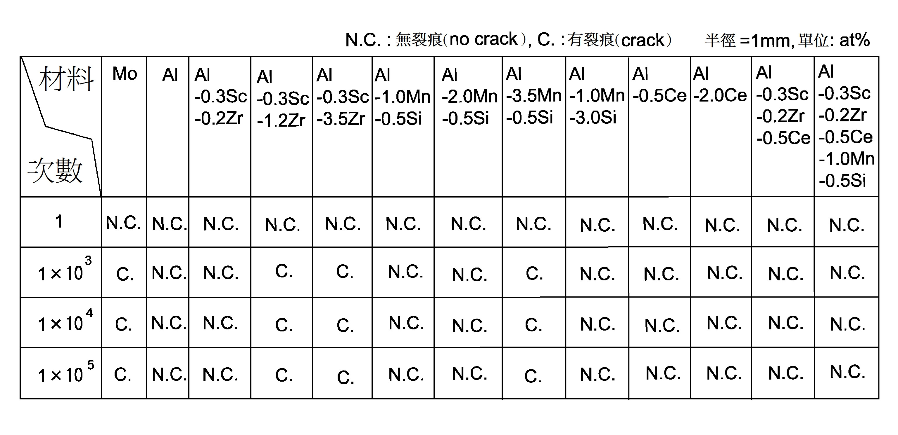
於表1係表示有Mo膜、Al膜及Al合金膜之撓曲特性的一例。濃度的單位是原子%(at%)。Table 1 shows an example of the flexural properties of the Mo film, Al film, and Al alloy film. The unit of concentration is atomic% (at%).
使用了兩層構造的SiN膜(200nm)、聚醯亞胺(polyimide)層(25μm)基板作為各樣本的基板。在撓曲試驗用的樣本中,Mo膜、Al膜及Al合金膜分別在SiN膜上濺鍍成膜。撓曲試驗裡的撓曲半徑係1 mm。試驗速度係30 rpm。依序進行了1次、1000次、10000次、100000次作為撓曲次數。裂痕(crack)的有無係以目視從光學顯微鏡的圖像判斷。A SiN film (200 nm) with a two-layer structure and a polyimide layer (25 μm) substrate were used as substrates for each sample. In the samples for the deflection test, the Mo film, the Al film, and the Al alloy film were formed by sputtering on the SiN film. The deflection radius in the deflection test is 1 mm. The test speed is 30 rpm. The number of deflections was 1 times, 1000 times, 10000 times, and 100,000 times in sequence. The presence or absence of cracks can be determined visually from the image of the optical microscope.
如表1所示,雖然在Al膜中以到100000次為止的撓曲次數都沒產生裂痕,但在Mo膜中以1000次的撓曲次數產生裂痕。關於Al合金膜,以到100000次為止的撓曲次數沒有產生裂痕。不過,在對Al純金屬添加了高於1.0 at%的1.5 at%之第一添加元素的情形下(Al-1.2 at%Zr-0.3 at%Sc),與在添加了高於3.0 at%的4.0 at%之第二添加元素的情形下(Al-3.5 at%Mn-0.5 at%Si),分別以1000次的撓曲次數產生裂痕。As shown in Table 1, although no cracks were generated in the Al film up to 100,000 flexing times, in the Mo film, cracks were generated in 1000 flexing times. Regarding the Al alloy film, cracks were not generated up to 100,000 deflection times. However, when the first added element of 1.5 at% higher than 1.0 at% is added to Al pure metal (Al-1.2 at%Zr-0.3 at%Sc), the In the case of 4.0 at% of the second added element (Al-3.5 at%Mn-0.5 at%Si), cracks were generated with 1000 deflections respectively.
[表2]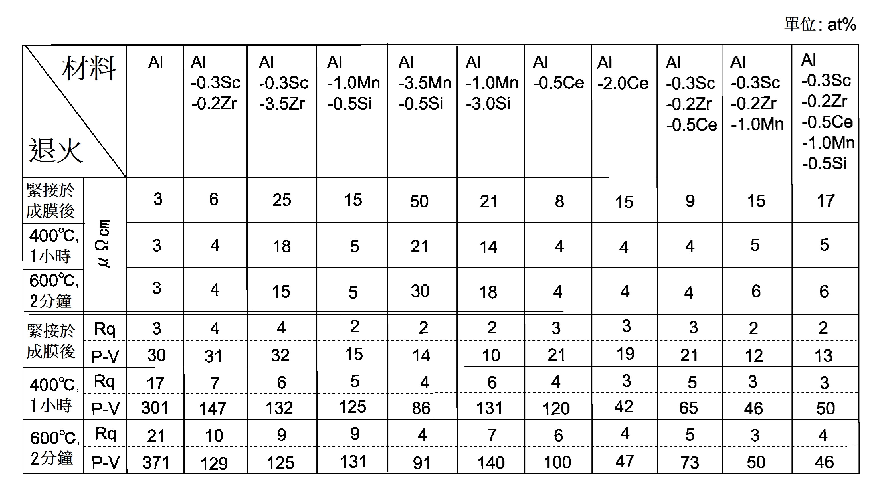
於表2係表示有Al膜及Al合金膜的比電阻(μΩ·cm)以及表面粗糙度(nm)之一例。 如表2所示,可以了解到在Al純金屬含有Sc、Zr之第一添加元素0.01 at%以上至1.0 at%以下時Al合金膜的比電阻會成為10μΩ·cm以下。又,可以了解到在Al純金屬含有Mn、Si之第二添加元素0.2 at%以上至3.0 at%以下時Al合金膜的比電阻也會成為10μΩ·cm以下。Table 2 shows an example of specific resistance (μΩ·cm) and surface roughness (nm) of Al film and Al alloy film. As shown in Table 2, it can be understood that the specific resistance of the Al alloy film becomes 10 μΩ·cm or less when the Al pure metal contains the first added elements of Sc and Zr from 0.01 at% or more to 1.0 at% or less. In addition, it can be understood that the specific resistance of the Al alloy film also becomes 10 μΩ·cm or less when the Al pure metal contains the second added elements of Mn and Si from 0.2 at% or more to 3.0 at% or less.
又,表面粗糙度係以AFM(Atomic Force Microscopy;原子力顯微術)來測定。表面粗糙度的觀測係在緊接於成膜後、以400℃在1小時後、以及以600℃在2分鐘後進行。測定範圍係5 μm正方。在各欄上段係顯示有Rq值(nm),在各欄下段係顯示有P-V值(nm)。此處,Rq值係平方平均數(root mean square)高度,P-V值係最大高處(峰值(peak))與最小低處(谷值(valley))的差。凸起愈成長P-V值就愈傾向於變高。在製造可靠性高的顯示設備時,配線膜的P-V值更小為佳,較佳為50 nm以下是理想的。特別是,藉由將P-V值為50 nm以下的Al合金膜應用在顯示面板之撓曲部分,就算Al合金膜彎曲,Al合金膜與上層的密合也是良好的。The surface roughness is measured by AFM (Atomic Force Microscopy; Atomic Force Microscopy). The observation of the surface roughness was performed immediately after the film formation, at 400°C for 1 hour, and at 600°C for 2 minutes. The measuring range is 5 μm square. The Rq value (nm) is displayed in the upper row of each column, and the P-V value (nm) is displayed in the lower row of each column. Here, the Rq value is the root mean square height, and the P-V value is the difference between the maximum high point (peak) and the minimum low point (valley). As the protrusion grows, the P-V value tends to become higher. When manufacturing a highly reliable display device, the P-V value of the wiring film is preferably smaller, preferably 50 nm or less. In particular, by applying an Al alloy film with a P-V value of 50 nm or less to the flexure of the display panel, even if the Al alloy film is bent, the adhesion of the Al alloy film to the upper layer is good.
如表2所示,在緊接於成膜後,Al膜、Al合金膜皆為表面粗糙度在50 nm以下。但是,在施予了加熱處理後,Al膜的P-V值係超過300 nm。另一方面,在Al合金膜中,P-V值都比Al膜還小。亦即,能夠判斷為與Al膜相比即使在Al合金膜中施予加熱處理亦不易在膜中成長凸起。As shown in Table 2, immediately after the film formation, both the Al film and the Al alloy film have a surface roughness below 50 nm. However, after the heat treatment was applied, the P-V value of the Al film exceeded 300 nm. On the other hand, in the Al alloy film, the P-V value is smaller than that of the Al film. That is, it can be judged that it is not easy to grow bumps in the Al alloy film even if heat treatment is applied to the Al alloy film compared to the Al film.
特別是,如Al-0.2 at%Zr-0.3 at%Sc-1.0 at%Mn、Al-0.5 at%Ce-0.2 at%Zr-0.3 at%Sc-1.0 at%Mn-0.5 at%Si般,可以了解到:藉由在Al純金屬一併添加第一添加元素與第二添加元素,就算施予加熱處理,表面粗糙度P-V值也會在50nm以下。這可以認為是:在Al合金膜中第一添加元素與第二添加元素相輔相成地作用,Al合金膜具備優異的對於熱負載之抗性。In particular, as Al-0.2 at%Zr-0.3 at%Sc-1.0 at%Mn, Al-0.5 at%Ce-0.2 at%Zr-0.3 at%Sc-1.0 at%Mn-0.5 at%Si, you can It is understood that by adding the first additive element and the second additive element to the Al pure metal together, even if heat treatment is applied, the PV value of the surface roughness will be below 50 nm. This is considered to be because the first additive element and the second additive element complement each other in the Al alloy film, and the Al alloy film has excellent resistance to thermal load.
[表3]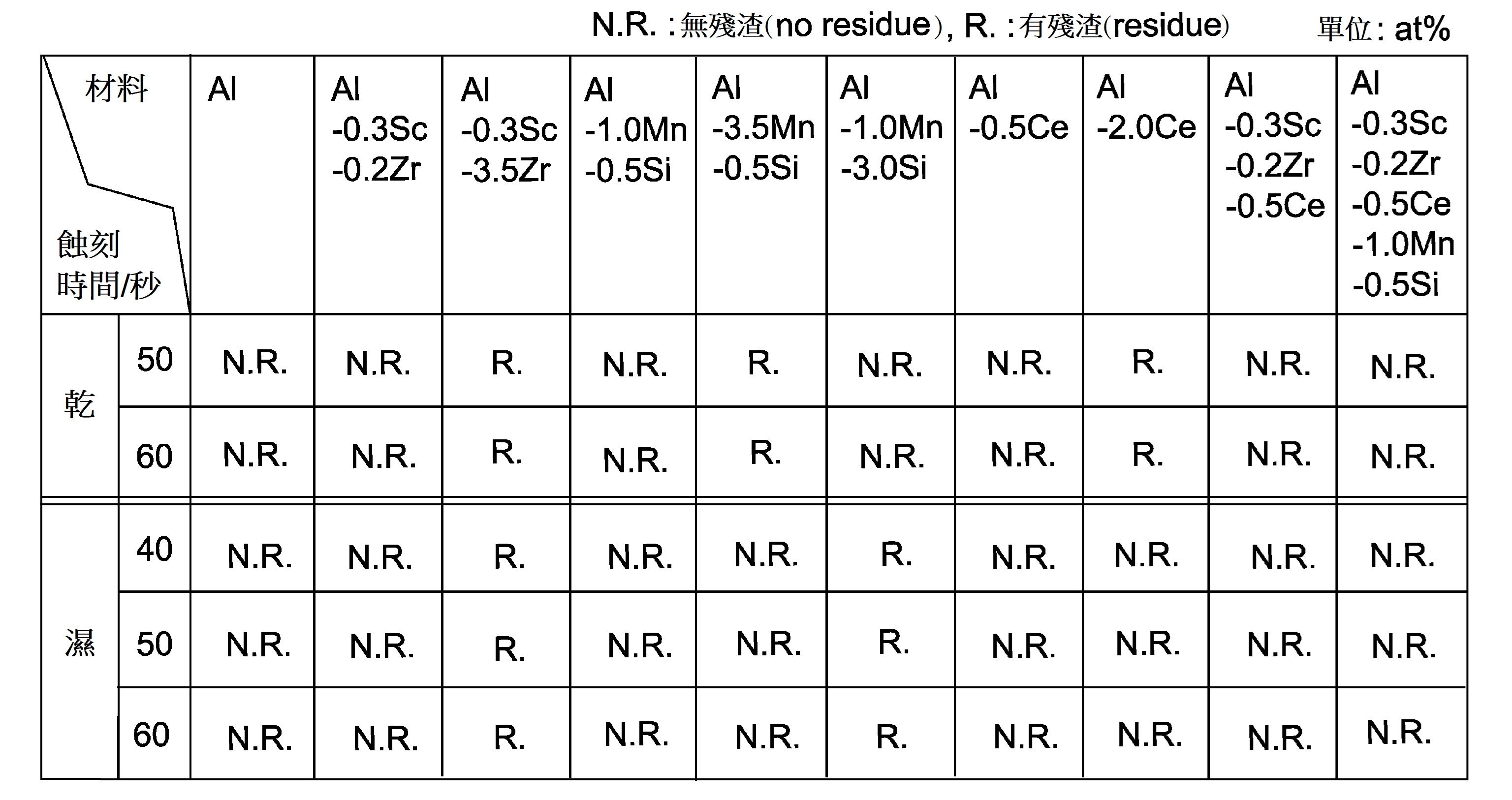
於表3係表示有在Al膜及Al合金膜的蝕刻後有無殘渣的一例。Table 3 shows an example of the presence or absence of residue after the etching of the Al film and Al alloy film.
在乾式蝕刻中,蝕刻氣體係Cl2 (50 sccm)、Ar(20 sccm)的混合氣體。蝕刻壓係1.0 Pa。放電電力在基板偏壓(bias)電力為200W之狀態下為400W。使用磷酸、硝酸、乙酸、水的混合溶液(通稱PAN(peroxyacetyl nitrate;過氧乙醯硝酸酯))作為濕式蝕刻液。液溫係40℃。In dry etching, a gas mixture of Cl 2 (50 sccm) and Ar (20 sccm) is etched. The etching pressure is 1.0 Pa. The discharge power is 400W in a state where the substrate bias power is 200W. A mixed solution of phosphoric acid, nitric acid, acetic acid, and water (commonly known as PAN (peroxyacetyl nitrate; peroxyacetyl nitrate)) is used as the wet etching solution. The liquid temperature is 40°C.
如表3所示,在含有屬於第三添加元素的Ce 0.5at%之Al合金膜(Al-0.5 at%Ce、Al-0.3 at%Sc-0.2 at%Zr-0.5 at%Ce、Al-0.3 at%Sc-0.2 at%Zr-0.5 at%Ce-1.0 at%Mn-0.5 at%Si)中,都能夠進行無殘渣的乾式蝕刻及濕式蝕刻。另一方面,在Ce的濃度變高且Ce為2.0 at%的Al合金膜(Al-2.0at%Ce)中,乾式蝕刻有殘渣產生。As shown in Table 3, the Al alloy film containing Ce 0.5at% belonging to the third additive element (Al-0.5 at%Ce, Al-0.3 at%Sc-0.2 at%Zr-0.5 at%Ce, Al-0.3 at%Sc-0.2 at%Zr-0.5 at%Ce-1.0 at%Mn-0.5 at%Si), both residue-free dry etching and wet etching can be performed. On the other hand, in an Al alloy film (Al-2.0 at% Ce) in which the concentration of Ce becomes high and Ce is 2.0 at%, residues are generated by dry etching.
另外,可以了解到在乾式蝕刻及濕式蝕刻中都有以下情形:在比較了Al-0.3 at%Sc-0.2 at%Zr與Al-0.3 at%Sc-3.5 at%Zr的情形下,於Zr的含有量多的Al-0.3 at%Sc-3.5 at%Zr中有殘渣產生。又,可以了解到:在乾式蝕刻中,在比較了Al-1.0 at%Mn-0.5 at%Si與Al-3.5 at%Mn-0.5 at%Si的情形下,於Mn的含有量多的Al-3.5 at%Mn-0.5 at%Si中有殘渣產生。另一方面,可以了解到:在濕式蝕刻中,在比較了Al-1.0 at%Mn-0.5 at%Si與Al-1.0 at%Mn-3.0 at%Si的情形下,於Si的含有量多的Al-1.0 at%Mn-3.0 at%Si中有殘渣產生。In addition, it can be understood that both dry etching and wet etching have the following situations: in the case of comparing Al-0.3 at%Sc-0.2 at%Zr and Al-0.3 at%Sc-3.5 at%Zr, in Zr A large amount of Al-0.3 at%Sc-3.5 at%Zr has residues. In addition, it can be understood that in dry etching, when Al-1.0 at%Mn-0.5 at%Si and Al-3.5 at%Mn-0.5 at%Si are compared, Al- Residues are generated in 3.5 at%Mn-0.5 at%Si. On the other hand, it can be understood that in wet etching, when Al-1.0 at%Mn-0.5 at%Si and Al-1.0 at%Mn-3.0 at%Si are compared, the content of Si is large Al-1.0 at%Mn-3.0 at%Si has residues.
(Al合金靶的具體例)(Specific example of Al alloy target)
例如,在坩堝設置有Al、Sc、Zr、Mn、Si及Ce各自的金屬材料(金屬片、金屬粉)。例如,以Al合金靶的添加元素之成分比成為0.2 at%Sc、0.1 at%Zr、1.0 at%Mn、0.5 at%Si及0.5 at%Ce的方式,在坩堝內設置各自的金屬材料(金屬片、金屬粉)。For example, metal materials (metal pieces, metal powders) of Al, Sc, Zr, Mn, Si, and Ce are provided in the crucible. For example, set the respective metal materials (metals in the crucible in such a way that the composition ratio of the added elements of the Al alloy target becomes 0.2 at%Sc, 0.1 at%Zr, 1.0 at%Mn, 0.5 at%Si and 0.5 at%Ce Film, metal powder).
接下來,藉由感應加熱,以比Al合金的熔點(例如640℃)還高400℃以上的熔融溫度(例如1050℃)對各金屬材料加熱,各金屬材料在坩堝內熔融。接下來,已熔融的金屬從該熔融溫度冷卻至室溫而形成鋁合金鑄錠。之後,依照需要鍛造鋁合金鑄錠,將鋁合金鑄錠切出成板狀或圓板狀。藉此形成Al合金靶。Next, by induction heating, each metal material is heated at a melting temperature (for example, 1050° C.) higher than the melting point of Al alloy (for example, 640° C.) by 400° C. or more, and each metal material is melted in the crucible. Next, the molten metal is cooled from the melting temperature to room temperature to form an aluminum alloy ingot. After that, the aluminum alloy ingot is forged as necessary, and the aluminum alloy ingot is cut into a plate shape or a disc shape. This forms an Al alloy target.
此處,以作為形成濺鍍靶用之合金鑄錠的方法而言有以下方法:以比金屬材料的熔點還高一些的熔融溫度將金屬材料予以熔融,將金屬材料從該比金屬材料的熔點還高一些的熔融溫度開始冷卻,以形成合金鑄錠。這是因為藉由縮短從熔融狀態到冷卻為止的冷卻時間來避免在冷卻過程產生的金屬間化合物的析出。但是,在此方法中,根據將熔融溫度設定成比熔點還高一些的溫度這點,金屬材料有可能無法充分地混合。Here, as a method of forming an alloy ingot for sputtering target, there is a method of melting a metal material at a melting temperature slightly higher than the melting point of the metal material, and removing the metal material from the melting point of the metal material The higher melting temperature begins to cool to form an alloy ingot. This is because the precipitation of intermetallic compounds generated during the cooling process is avoided by shortening the cooling time from the molten state to the cooling. However, in this method, depending on the fact that the melting temperature is set to a temperature slightly higher than the melting point, the metal materials may not be sufficiently mixed.
相對於此,在本實施例中,由於是以比Al合金的熔點還高400℃以上的熔融溫度將金屬材料予以加熱熔融,故各個金屬材料充分地互相混合。此處,熔融溫度變得愈高從熔融溫度到室溫為止的冷卻時間就變得愈長,可認為金屬間化合物就愈容易析出。但是,在本實施形態中,以就算Al合金鑄錠從比這樣的Al合金的熔點還高400℃以上之熔融溫度開始冷卻也不易在Al合金鑄錠中析出金屬間化合物之方式調整添加元素的濃度。On the other hand, in this embodiment, since the metal materials are heated and melted at a melting temperature higher than the melting point of the Al alloy by 400° C. or higher, the respective metal materials are sufficiently mixed with each other. Here, as the melting temperature becomes higher, the cooling time from the melting temperature to room temperature becomes longer, and it is considered that the intermetallic compound is more likely to precipitate. However, in the present embodiment, even if the Al alloy ingot is cooled from a melting temperature higher than the melting point of such an Al alloy by 400° C. or more, it is difficult to adjust the additive elements such that intermetallic compounds are precipitated in the Al alloy ingot. concentration.
圖2是說明表4所例示之Al合金鑄錠的組成分析之觀測點的概念圖。 表4係表示Al合金鑄錠所含的各元素之濃度分布的一例。FIG. 2 is a conceptual diagram illustrating observation points of the composition analysis of the Al alloy ingot illustrated in Table 4. FIG. Table 4 shows an example of the concentration distribution of each element contained in the Al alloy ingot.
[表4]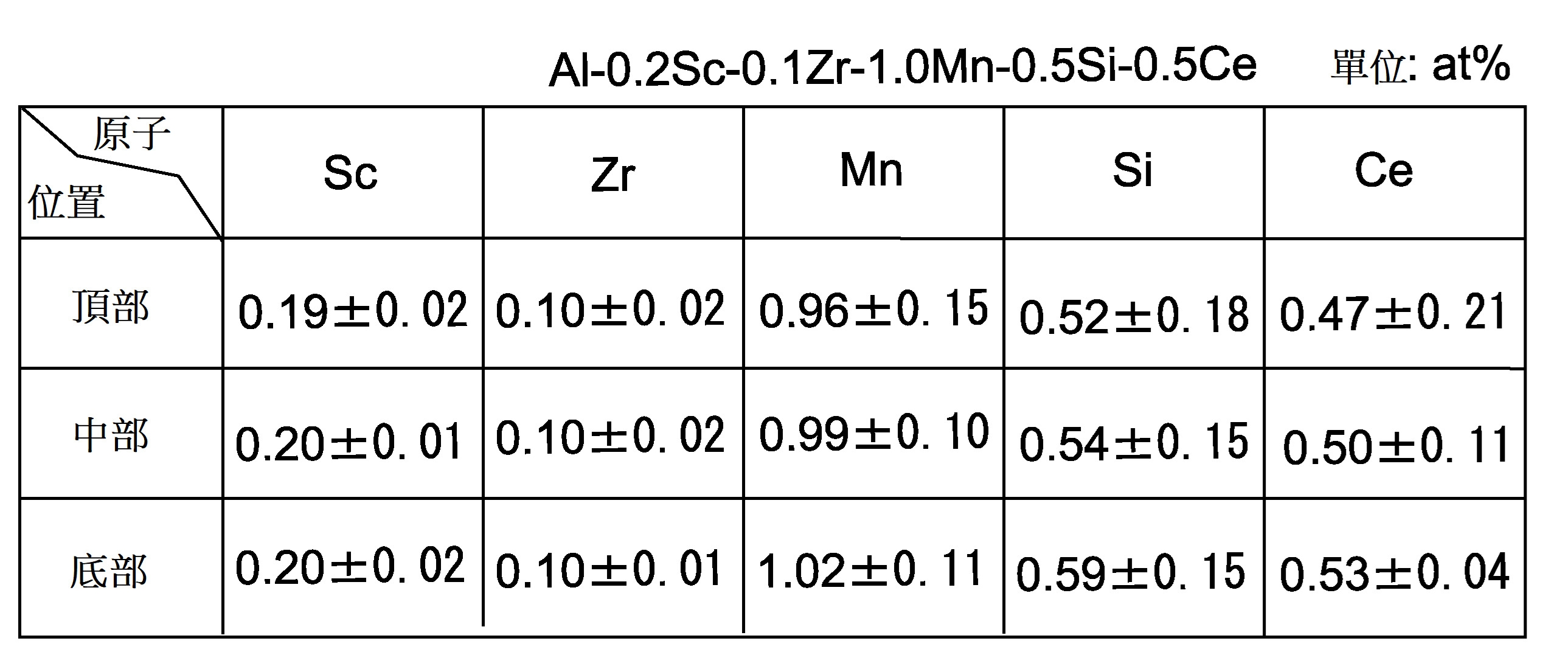
於圖2係例示有將例如圓柱狀的Al合金鑄錠(100mm徑×50 mmt)分割成兩個而成的半圓柱狀的Al合金鑄錠5。FIG. 2 illustrates an example of a semi-cylindrical
以作為在Al合金鑄錠5中的組成分析之觀測點而言,在頂部(top)的位置於橫方向等間隔地選擇九點、在中部(middle)的位置於橫方向等間隔地選擇九點、以及在底部(bottom)的位置於橫方向等間隔地選擇九點,合計選擇二十七點。於表4係表示有在頂部的位置對各元素從九點觀測點所測定的平均值濃度(at%)、在中部的位置對各元素從九點觀測點所測定的平均值濃度(at%)、以及在底部的位置對各元素從九點觀測點所測定的平均值濃度(at%)。於表4也表示有濃度的平均值之偏差±3σ。As an observation point for the composition analysis in the
如表4所示,可以了解到:Al合金鑄錠之添加元素的成分比在頂部、中部及底部之任一位置皆變成Sc為0.2 at%、Zr為0.1 at%、Mn為1.0 at%、Si為0.5 at%、Ce為0.5 at%左右,且在Al合金鑄錠中,各金屬材料在Al合金鑄錠的縱方向及橫方向均勻地分散。As shown in Table 4, it can be understood that the composition ratio of the added element of the Al alloy ingot becomes Sc at 0.2 at%, Zr at 0.1 at%, Mn at 1.0 at% at any position of the top, middle and bottom. Si is 0.5 at% and Ce is about 0.5 at%, and in the Al alloy ingot, each metal material is uniformly dispersed in the longitudinal direction and the lateral direction of the Al alloy ingot.
[表5]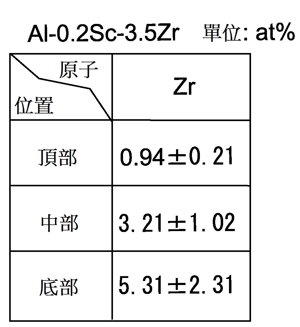
相對於此,將在添加了Sc 0.2 at%、Zr 3.5 at%之情形下的鋁合金鑄錠之Zr濃度分布表示於表5。製造方法係與表4所示的鋁合金鑄錠相同。如表5所示,可以了解到當使Zr濃度增加到3.5 at%時,Zr濃度隨著從鋁合金鑄錠的頂部往底部而變高。將在此情形下的光學顯微鏡像表示於圖3。On the other hand, the Zr concentration distribution of the aluminum alloy ingot when Sc 0.2 at% and Zr 3.5 at% are added is shown in Table 5. The manufacturing method is the same as the aluminum alloy ingot shown in Table 4. As shown in Table 5, it can be understood that when the Zr concentration is increased to 3.5 at%, the Zr concentration becomes higher from the top to the bottom of the aluminum alloy ingot. The optical microscope image in this case is shown in FIG. 3.
圖3是表5所示的鋁合金鑄錠之光學顯微鏡像。3 is an optical microscope image of the aluminum alloy ingot shown in Table 5.
如圖3所示,可以了解到在表5所示的鋁合金鑄錠中存在粒徑為數百μm左右的結晶粒(金屬間化合物)。As shown in FIG. 3, it can be understood that there are crystal grains (intermetallic compounds) having a particle size of about several hundred μm in the aluminum alloy ingot shown in Table 5.
圖4中的(a)、(b)是本實施形態之鋁合金鑄錠的電子顯微鏡像。(A) and (b) in FIG. 4 are electron microscope images of the aluminum alloy ingot of this embodiment.
於圖4中的(a)係表示有表4所示的鋁合金鑄錠之表面電子顯微鏡像。又,於圖4中的(b)係表示有對表4所示的鋁合金鑄錠進行600℃、2小時之加熱處理後的鋁合金鑄錠之表面電子顯微鏡像。在圖4中的(a)、(b)中的右圖像是將左圖像的比例(scale)放大而成的圖像。(A) in FIG. 4 shows the surface electron microscope image of the aluminum alloy ingot shown in Table 4. In addition, (b) in FIG. 4 shows a surface electron microscope image of the aluminum alloy ingot after heat treatment of the aluminum alloy ingot shown in Table 4 at 600° C. for 2 hours. The right image in (a) and (b) in FIG. 4 is an image obtained by enlarging the scale of the left image.
如圖4中的(a)左邊所示,緊接在製作了鋁合金鑄錠之後,沒觀察到粒徑為數百μm左右的結晶粒(金屬間化合物)。但是,如圖4中的(a)右邊所示,鋁合金鑄錠係由平均粒徑10μm左右的粒子A之群集所構成。接下來,若以EDX(energy dispersive X-ray;能量色散X射線)分析將粒子A間的粒界B之成分予以解析,則在粒界B觀測到Ce、Mn及Si為高濃度。也就是說,可以了解到以下情形:在粒子A間的粒界中的Ce、Mn及Si之至少任一者的含有量係比在粒子A內的Ce、Mn及Si之至少任一者的含有量還高。As shown on the left side of (a) in FIG. 4, immediately after the aluminum alloy ingot was produced, crystal grains (intermetallic compounds) with a particle size of about several hundred μm were not observed. However, as shown on the right of (a) in FIG. 4, the aluminum alloy ingot is composed of clusters of particles A having an average particle diameter of about 10 μm. Next, if the composition of the grain boundary B between the particles A is analyzed by EDX (energy dispersive X-ray) analysis, Ce, Mn, and Si are observed at high concentrations in the grain boundary B. That is, it can be understood that the content of at least any one of Ce, Mn, and Si in the grain boundary between particles A is higher than that of at least any one of Ce, Mn, and Si in particles A The content is still high.
又,將從圖4中的(a)之狀態進行了600℃、2小時的加熱處理之圖像表示於圖4中的(b)。在此情形下粒徑也是止於10μm左右,沒有粒子A彼此結合而成長為巨大的粒子,或在粒子A內析出新的粒子(例如金屬間化合物)之情形。由此能夠預測:在Al合金鑄錠中粒界B成為障壁,抑制了鄰接的粒子A連繋而粒子粗大化的現象,並且在粒子A內Zr、Sc均勻地分散,粒成長已被抑制。結果,可認為Al合金靶的耐熱性提升了。In addition, an image of heat treatment at 600°C for 2 hours from the state of (a) in FIG. 4 is shown in (b) of FIG. 4. In this case, the particle size is also limited to about 10 μm, and there is no case where the particles A are bound to each other to grow into huge particles, or new particles (such as intermetallic compounds) are precipitated in the particles A. From this, it can be predicted that the grain boundary B becomes a barrier in the Al alloy ingot, the phenomenon that the adjacent particles A are connected and the particles are coarsened is suppressed, and Zr and Sc are uniformly dispersed in the particles A, and the grain growth is suppressed. As a result, it is considered that the heat resistance of the Al alloy target is improved.
以上,對本發明的實施形態進行了說明,不過本發明並非僅限定於上述實施形態,當然能夠施加各種變更。各實施形態並不限於獨立的形態,只要技術上可能則能夠進行複合。The embodiments of the present invention have been described above, but the present invention is not limited to the above-mentioned embodiments, and of course various modifications can be added. Each embodiment is not limited to an independent form, and can be compounded as long as technically possible.
例如,雖然在以上的實施形態中表示了將Al合金膜應用於閘極電極13、23的例子,但也能夠將Al合金膜應用於源極/汲極電極、源極/汲極電極以外的其他電極或配線。For example, although the above embodiment shows an example in which the Al alloy film is applied to the
1、2‧‧‧薄膜電晶體
5‧‧‧Al合金鑄錠
10、20‧‧‧玻璃基板
11、21‧‧‧活性層
12、22‧‧‧閘極絕緣膜
13、23‧‧‧閘極電極
15‧‧‧保護層
16D、26D‧‧‧汲極電極
16S、26S‧‧‧源極電極
A‧‧‧粒子
B‧‧‧粒界
1, 2‧‧‧
圖1是具有本實施形態之Al合金膜的薄膜電晶體之概略剖視圖。 圖2是用以說明表4所例示的Al合金鑄錠(ingot)之組成分析的觀測點之概念圖。 圖3是表5所示的鋁合金鑄錠之光學顯微鏡像。 圖4是本實施形態之鋁合金鑄錠的電子顯微鏡像。FIG. 1 is a schematic cross-sectional view of a thin film transistor having an Al alloy film of this embodiment. FIG. 2 is a conceptual diagram for explaining the observation points of the composition analysis of the Al alloy ingot illustrated in Table 4. FIG. 3 is an optical microscope image of the aluminum alloy ingot shown in Table 5. 4 is an electron microscope image of the aluminum alloy ingot of this embodiment.
1、2‧‧‧薄膜電晶體 1, 2‧‧‧ thin film transistor
10、20‧‧‧玻璃基板 10, 20‧‧‧ glass substrate
11、21‧‧‧活性層 11, 21‧‧‧ active layer
12、22‧‧‧閘極絕緣膜 12, 22‧‧‧ Gate insulating film
13、23‧‧‧閘極電極 13, 23‧‧‧ Gate electrode
15‧‧‧保護層 15‧‧‧Protective layer
16D、26D‧‧‧汲極電極 16D, 26D‧‧‧Drain electrode
16S、26S‧‧‧源極電極 16S, 26S‧‧‧Source electrode
Claims (11)
Applications Claiming Priority (2)
| Application Number | Priority Date | Filing Date | Title |
|---|---|---|---|
| JP2018123157 | 2018-06-28 | ||
| JP2018-123157 | 2018-06-28 |
Publications (2)
| Publication Number | Publication Date |
|---|---|
| TW202000941A true TW202000941A (en) | 2020-01-01 |
| TWI738005B TWI738005B (en) | 2021-09-01 |
Family
ID=68986972
Family Applications (1)
| Application Number | Title | Priority Date | Filing Date |
|---|---|---|---|
| TW108120573A TWI738005B (en) | 2018-06-28 | 2019-06-14 | Aluminum alloy film, manufacturing method for the same, and thin film transistor |
Country Status (6)
| Country | Link |
|---|---|
| US (1) | US11935936B2 (en) |
| JP (1) | JP6842562B2 (en) |
| KR (1) | KR102549527B1 (en) |
| CN (1) | CN112262222B (en) |
| TW (1) | TWI738005B (en) |
| WO (1) | WO2020003667A1 (en) |
Families Citing this family (6)
| Publication number | Priority date | Publication date | Assignee | Title |
|---|---|---|---|---|
| JP6735930B2 (en) * | 2018-06-28 | 2020-08-05 | 株式会社アルバック | Aluminum alloy target and manufacturing method thereof |
| KR102474944B1 (en) * | 2020-04-08 | 2022-12-06 | 주식회사 큐프럼 머티리얼즈 | Manufacturing method of wiring film, wiring film and display device using the same |
| TW202318568A (en) * | 2021-07-30 | 2023-05-01 | 日商尼康股份有限公司 | Method for manufacturing metal wiring, method for manufacturing transistor, and metal wiring |
| KR102865855B1 (en) * | 2021-12-30 | 2025-09-30 | 주식회사 큐프럼 머티리얼즈 | Alloy Composition Comprising Aluminum, Manganese, Titanium and Silicon for Thin Film Transistor Electrodes and Reflective Electrodes |
| JP2023173191A (en) | 2022-05-25 | 2023-12-07 | ルネサスエレクトロニクス株式会社 | Semiconductor device and its manufacturing method |
| WO2024167046A1 (en) * | 2023-02-10 | 2024-08-15 | 주식회사 큐프럼 머티리얼즈 | Thin film transistor electrode, and alloy composition comprising aluminum, manganese, titanium, and silicon for reflective electrode |
Family Cites Families (15)
| Publication number | Priority date | Publication date | Assignee | Title |
|---|---|---|---|---|
| JP4137182B2 (en) | 1995-10-12 | 2008-08-20 | 株式会社東芝 | Sputter target for wiring film formation |
| USRE45481E1 (en) * | 1995-10-12 | 2015-04-21 | Kabushiki Kaisha Toshiba | Interconnector line of thin film, sputter target for forming the wiring film and electronic component using the same |
| US20010047838A1 (en) | 2000-03-28 | 2001-12-06 | Segal Vladimir M. | Methods of forming aluminum-comprising physical vapor deposition targets; sputtered films; and target constructions |
| JP4783525B2 (en) * | 2001-08-31 | 2011-09-28 | 株式会社アルバック | Thin film aluminum alloy and sputtering target for forming thin film aluminum alloy |
| JP3940385B2 (en) * | 2002-12-19 | 2007-07-04 | 株式会社神戸製鋼所 | Display device and manufacturing method thereof |
| JP4237479B2 (en) | 2002-12-25 | 2009-03-11 | 株式会社東芝 | Sputtering target, Al alloy film and electronic parts |
| JP4022891B2 (en) | 2003-11-20 | 2007-12-19 | 日立金属株式会社 | Al alloy film for wiring film and sputtering target material for forming wiring film |
| US7166921B2 (en) | 2003-11-20 | 2007-01-23 | Hitachi Metals, Ltd. | Aluminum alloy film for wiring and sputter target material for forming the film |
| WO2009123217A1 (en) | 2008-03-31 | 2009-10-08 | 株式会社神戸製鋼所 | Display device, process for producing the display device, and sputtering target |
| JP5179604B2 (en) * | 2010-02-16 | 2013-04-10 | 株式会社神戸製鋼所 | Al alloy film for display devices |
| JP5032687B2 (en) * | 2010-09-30 | 2012-09-26 | 株式会社神戸製鋼所 | Al alloy film, wiring structure having Al alloy film, and sputtering target used for production of Al alloy film |
| JP2012180540A (en) * | 2011-02-28 | 2012-09-20 | Kobe Steel Ltd | Al ALLOY FILM FOR DISPLAY DEVICE AND SEMICONDUCTOR DEVICE |
| JP5524905B2 (en) | 2011-05-17 | 2014-06-18 | 株式会社神戸製鋼所 | Al alloy film for power semiconductor devices |
| US9803283B1 (en) * | 2013-10-18 | 2017-10-31 | Hrl Laboratories, Llc | Method of electroless deposition of aluminum or aluminum alloy, an electroless plating composition, and an article including the same |
| CN105917450A (en) | 2014-01-15 | 2016-08-31 | 株式会社神户制钢所 | Thin-film transistor |
-
2019
- 2019-03-28 WO PCT/JP2019/013570 patent/WO2020003667A1/en not_active Ceased
- 2019-03-28 CN CN201980039161.2A patent/CN112262222B/en active Active
- 2019-03-28 JP JP2019547523A patent/JP6842562B2/en active Active
- 2019-03-28 US US17/055,852 patent/US11935936B2/en active Active
- 2019-03-28 KR KR1020207037510A patent/KR102549527B1/en active Active
- 2019-06-14 TW TW108120573A patent/TWI738005B/en active
Also Published As
| Publication number | Publication date |
|---|---|
| JP6842562B2 (en) | 2021-03-17 |
| WO2020003667A1 (en) | 2020-01-02 |
| CN112262222B (en) | 2023-06-06 |
| US11935936B2 (en) | 2024-03-19 |
| US20210226028A1 (en) | 2021-07-22 |
| CN112262222A (en) | 2021-01-22 |
| KR20210013220A (en) | 2021-02-03 |
| KR102549527B1 (en) | 2023-06-28 |
| JPWO2020003667A1 (en) | 2020-07-02 |
| TWI738005B (en) | 2021-09-01 |
Similar Documents
| Publication | Publication Date | Title |
|---|---|---|
| TWI738005B (en) | Aluminum alloy film, manufacturing method for the same, and thin film transistor | |
| CN100392505C (en) | Copper alloy film, copper alloy sputtering target and flat panel display | |
| KR101376502B1 (en) | Sputtering target | |
| TWI766163B (en) | Aluminum alloy target and manufacturing method for the same | |
| TWI826799B (en) | Metal wiring structure and method for manufacturing metal wiring structure | |
| TWI749780B (en) | Aluminum alloy target, aluminum alloy wiring film, and method for manufacturing aluminum alloy wiring film | |
| JP6947604B2 (en) | Method for manufacturing Al alloy conductive film, thin film transistor and Al alloy conductive film | |
| TWI619820B (en) | Copper alloy sputtering target | |
| JP5510812B2 (en) | Cu alloy film for wiring film and sputtering target material for forming wiring film |