WO2020003667A1 - Aluminum alloy film, method for producing same, and thin film transistor - Google Patents
Aluminum alloy film, method for producing same, and thin film transistor Download PDFInfo
- Publication number
- WO2020003667A1 WO2020003667A1 PCT/JP2019/013570 JP2019013570W WO2020003667A1 WO 2020003667 A1 WO2020003667 A1 WO 2020003667A1 JP 2019013570 W JP2019013570 W JP 2019013570W WO 2020003667 A1 WO2020003667 A1 WO 2020003667A1
- Authority
- WO
- WIPO (PCT)
- Prior art keywords
- alloy film
- atomic
- aluminum alloy
- additive element
- alloy
- Prior art date
- Legal status (The legal status is an assumption and is not a legal conclusion. Google has not performed a legal analysis and makes no representation as to the accuracy of the status listed.)
- Ceased
Links
Images
Classifications
-
- C—CHEMISTRY; METALLURGY
- C23—COATING METALLIC MATERIAL; COATING MATERIAL WITH METALLIC MATERIAL; CHEMICAL SURFACE TREATMENT; DIFFUSION TREATMENT OF METALLIC MATERIAL; COATING BY VACUUM EVAPORATION, BY SPUTTERING, BY ION IMPLANTATION OR BY CHEMICAL VAPOUR DEPOSITION, IN GENERAL; INHIBITING CORROSION OF METALLIC MATERIAL OR INCRUSTATION IN GENERAL
- C23C—COATING METALLIC MATERIAL; COATING MATERIAL WITH METALLIC MATERIAL; SURFACE TREATMENT OF METALLIC MATERIAL BY DIFFUSION INTO THE SURFACE, BY CHEMICAL CONVERSION OR SUBSTITUTION; COATING BY VACUUM EVAPORATION, BY SPUTTERING, BY ION IMPLANTATION OR BY CHEMICAL VAPOUR DEPOSITION, IN GENERAL
- C23C14/00—Coating by vacuum evaporation, by sputtering or by ion implantation of the coating forming material
- C23C14/22—Coating by vacuum evaporation, by sputtering or by ion implantation of the coating forming material characterised by the process of coating
- C23C14/34—Sputtering
- C23C14/3407—Cathode assembly for sputtering apparatus, e.g. Target
- C23C14/3414—Metallurgical or chemical aspects of target preparation, e.g. casting, powder metallurgy
-
- H—ELECTRICITY
- H10—SEMICONDUCTOR DEVICES; ELECTRIC SOLID-STATE DEVICES NOT OTHERWISE PROVIDED FOR
- H10D—INORGANIC ELECTRIC SEMICONDUCTOR DEVICES
- H10D64/00—Electrodes of devices having potential barriers
- H10D64/60—Electrodes characterised by their materials
- H10D64/66—Electrodes having a conductor capacitively coupled to a semiconductor by an insulator, e.g. MIS electrodes
-
- C—CHEMISTRY; METALLURGY
- C22—METALLURGY; FERROUS OR NON-FERROUS ALLOYS; TREATMENT OF ALLOYS OR NON-FERROUS METALS
- C22C—ALLOYS
- C22C21/00—Alloys based on aluminium
-
- C—CHEMISTRY; METALLURGY
- C22—METALLURGY; FERROUS OR NON-FERROUS ALLOYS; TREATMENT OF ALLOYS OR NON-FERROUS METALS
- C22F—CHANGING THE PHYSICAL STRUCTURE OF NON-FERROUS METALS AND NON-FERROUS ALLOYS
- C22F1/00—Changing the physical structure of non-ferrous metals or alloys by heat treatment or by hot or cold working
- C22F1/04—Changing the physical structure of non-ferrous metals or alloys by heat treatment or by hot or cold working of aluminium or alloys based thereon
-
- C—CHEMISTRY; METALLURGY
- C23—COATING METALLIC MATERIAL; COATING MATERIAL WITH METALLIC MATERIAL; CHEMICAL SURFACE TREATMENT; DIFFUSION TREATMENT OF METALLIC MATERIAL; COATING BY VACUUM EVAPORATION, BY SPUTTERING, BY ION IMPLANTATION OR BY CHEMICAL VAPOUR DEPOSITION, IN GENERAL; INHIBITING CORROSION OF METALLIC MATERIAL OR INCRUSTATION IN GENERAL
- C23C—COATING METALLIC MATERIAL; COATING MATERIAL WITH METALLIC MATERIAL; SURFACE TREATMENT OF METALLIC MATERIAL BY DIFFUSION INTO THE SURFACE, BY CHEMICAL CONVERSION OR SUBSTITUTION; COATING BY VACUUM EVAPORATION, BY SPUTTERING, BY ION IMPLANTATION OR BY CHEMICAL VAPOUR DEPOSITION, IN GENERAL
- C23C14/00—Coating by vacuum evaporation, by sputtering or by ion implantation of the coating forming material
- C23C14/06—Coating by vacuum evaporation, by sputtering or by ion implantation of the coating forming material characterised by the coating material
- C23C14/14—Metallic material, boron or silicon
-
- C—CHEMISTRY; METALLURGY
- C23—COATING METALLIC MATERIAL; COATING MATERIAL WITH METALLIC MATERIAL; CHEMICAL SURFACE TREATMENT; DIFFUSION TREATMENT OF METALLIC MATERIAL; COATING BY VACUUM EVAPORATION, BY SPUTTERING, BY ION IMPLANTATION OR BY CHEMICAL VAPOUR DEPOSITION, IN GENERAL; INHIBITING CORROSION OF METALLIC MATERIAL OR INCRUSTATION IN GENERAL
- C23C—COATING METALLIC MATERIAL; COATING MATERIAL WITH METALLIC MATERIAL; SURFACE TREATMENT OF METALLIC MATERIAL BY DIFFUSION INTO THE SURFACE, BY CHEMICAL CONVERSION OR SUBSTITUTION; COATING BY VACUUM EVAPORATION, BY SPUTTERING, BY ION IMPLANTATION OR BY CHEMICAL VAPOUR DEPOSITION, IN GENERAL
- C23C26/00—Coating not provided for in groups C23C2/00 - C23C24/00
-
- H—ELECTRICITY
- H10—SEMICONDUCTOR DEVICES; ELECTRIC SOLID-STATE DEVICES NOT OTHERWISE PROVIDED FOR
- H10D—INORGANIC ELECTRIC SEMICONDUCTOR DEVICES
- H10D30/00—Field-effect transistors [FET]
- H10D30/60—Insulated-gate field-effect transistors [IGFET]
- H10D30/67—Thin-film transistors [TFT]
-
- H—ELECTRICITY
- H10—SEMICONDUCTOR DEVICES; ELECTRIC SOLID-STATE DEVICES NOT OTHERWISE PROVIDED FOR
- H10D—INORGANIC ELECTRIC SEMICONDUCTOR DEVICES
- H10D30/00—Field-effect transistors [FET]
- H10D30/60—Insulated-gate field-effect transistors [IGFET]
- H10D30/67—Thin-film transistors [TFT]
- H10D30/6729—Thin-film transistors [TFT] characterised by the electrodes
- H10D30/673—Thin-film transistors [TFT] characterised by the electrodes characterised by the shapes, relative sizes or dispositions of the gate electrodes
-
- H—ELECTRICITY
- H10—SEMICONDUCTOR DEVICES; ELECTRIC SOLID-STATE DEVICES NOT OTHERWISE PROVIDED FOR
- H10D—INORGANIC ELECTRIC SEMICONDUCTOR DEVICES
- H10D30/00—Field-effect transistors [FET]
- H10D30/60—Insulated-gate field-effect transistors [IGFET]
- H10D30/67—Thin-film transistors [TFT]
- H10D30/6729—Thin-film transistors [TFT] characterised by the electrodes
- H10D30/6737—Thin-film transistors [TFT] characterised by the electrodes characterised by the electrode materials
- H10D30/6739—Conductor-insulator-semiconductor electrodes
-
- H—ELECTRICITY
- H10—SEMICONDUCTOR DEVICES; ELECTRIC SOLID-STATE DEVICES NOT OTHERWISE PROVIDED FOR
- H10D—INORGANIC ELECTRIC SEMICONDUCTOR DEVICES
- H10D64/00—Electrodes of devices having potential barriers
- H10D64/01—Manufacture or treatment
- H10D64/011—Manufacture or treatment of electrodes ohmically coupled to a semiconductor
-
- H—ELECTRICITY
- H10—SEMICONDUCTOR DEVICES; ELECTRIC SOLID-STATE DEVICES NOT OTHERWISE PROVIDED FOR
- H10D—INORGANIC ELECTRIC SEMICONDUCTOR DEVICES
- H10D64/00—Electrodes of devices having potential barriers
- H10D64/01—Manufacture or treatment
- H10D64/013—Manufacture or treatment of electrodes having a conductor capacitively coupled to a semiconductor by an insulator
- H10D64/01302—Manufacture or treatment of electrodes having a conductor capacitively coupled to a semiconductor by an insulator the insulator being formed after the semiconductor body, the semiconductor being silicon
- H10D64/01304—Manufacture or treatment of electrodes having a conductor capacitively coupled to a semiconductor by an insulator the insulator being formed after the semiconductor body, the semiconductor being silicon characterised by the conductor
- H10D64/01318—Manufacture or treatment of electrodes having a conductor capacitively coupled to a semiconductor by an insulator the insulator being formed after the semiconductor body, the semiconductor being silicon characterised by the conductor the conductor comprising a layer of alloy material, compound material or organic material contacting the insulator, e.g. TiN
-
- H—ELECTRICITY
- H10—SEMICONDUCTOR DEVICES; ELECTRIC SOLID-STATE DEVICES NOT OTHERWISE PROVIDED FOR
- H10D—INORGANIC ELECTRIC SEMICONDUCTOR DEVICES
- H10D64/00—Electrodes of devices having potential barriers
- H10D64/60—Electrodes characterised by their materials
- H10D64/66—Electrodes having a conductor capacitively coupled to a semiconductor by an insulator, e.g. MIS electrodes
- H10D64/667—Electrodes having a conductor capacitively coupled to a semiconductor by an insulator, e.g. MIS electrodes the conductor comprising a layer of alloy material, compound material or organic material contacting the insulator, e.g. TiN workfunction layers
-
- H—ELECTRICITY
- H10—SEMICONDUCTOR DEVICES; ELECTRIC SOLID-STATE DEVICES NOT OTHERWISE PROVIDED FOR
- H10P—GENERIC PROCESSES OR APPARATUS FOR THE MANUFACTURE OR TREATMENT OF DEVICES COVERED BY CLASS H10
- H10P14/00—Formation of materials, e.g. in the shape of layers or pillars
- H10P14/40—Formation of materials, e.g. in the shape of layers or pillars of conductive or resistive materials
- H10P14/42—Formation of materials, e.g. in the shape of layers or pillars of conductive or resistive materials using a gas or vapour
-
- H—ELECTRICITY
- H10—SEMICONDUCTOR DEVICES; ELECTRIC SOLID-STATE DEVICES NOT OTHERWISE PROVIDED FOR
- H10P—GENERIC PROCESSES OR APPARATUS FOR THE MANUFACTURE OR TREATMENT OF DEVICES COVERED BY CLASS H10
- H10P14/00—Formation of materials, e.g. in the shape of layers or pillars
- H10P14/40—Formation of materials, e.g. in the shape of layers or pillars of conductive or resistive materials
- H10P14/42—Formation of materials, e.g. in the shape of layers or pillars of conductive or resistive materials using a gas or vapour
- H10P14/44—Physical vapour deposition [PVD]
-
- H—ELECTRICITY
- H10—SEMICONDUCTOR DEVICES; ELECTRIC SOLID-STATE DEVICES NOT OTHERWISE PROVIDED FOR
- H10W—GENERIC PACKAGES, INTERCONNECTIONS, CONNECTORS OR OTHER CONSTRUCTIONAL DETAILS OF DEVICES COVERED BY CLASS H10
- H10W20/00—Interconnections in chips, wafers or substrates
- H10W20/40—Interconnections external to wafers or substrates, e.g. back-end-of-line [BEOL] metallisations or vias connecting to gate electrodes
- H10W20/41—Interconnections external to wafers or substrates, e.g. back-end-of-line [BEOL] metallisations or vias connecting to gate electrodes characterised by their conductive parts
- H10W20/44—Conductive materials thereof
- H10W20/4403—Conductive materials thereof based on metals, e.g. alloys, metal silicides
- H10W20/4405—Conductive materials thereof based on metals, e.g. alloys, metal silicides the principal metal being aluminium
- H10W20/4407—Aluminium alloys
-
- C—CHEMISTRY; METALLURGY
- C22—METALLURGY; FERROUS OR NON-FERROUS ALLOYS; TREATMENT OF ALLOYS OR NON-FERROUS METALS
- C22F—CHANGING THE PHYSICAL STRUCTURE OF NON-FERROUS METALS AND NON-FERROUS ALLOYS
- C22F1/00—Changing the physical structure of non-ferrous metals or alloys by heat treatment or by hot or cold working
-
- C—CHEMISTRY; METALLURGY
- C23—COATING METALLIC MATERIAL; COATING MATERIAL WITH METALLIC MATERIAL; CHEMICAL SURFACE TREATMENT; DIFFUSION TREATMENT OF METALLIC MATERIAL; COATING BY VACUUM EVAPORATION, BY SPUTTERING, BY ION IMPLANTATION OR BY CHEMICAL VAPOUR DEPOSITION, IN GENERAL; INHIBITING CORROSION OF METALLIC MATERIAL OR INCRUSTATION IN GENERAL
- C23C—COATING METALLIC MATERIAL; COATING MATERIAL WITH METALLIC MATERIAL; SURFACE TREATMENT OF METALLIC MATERIAL BY DIFFUSION INTO THE SURFACE, BY CHEMICAL CONVERSION OR SUBSTITUTION; COATING BY VACUUM EVAPORATION, BY SPUTTERING, BY ION IMPLANTATION OR BY CHEMICAL VAPOUR DEPOSITION, IN GENERAL
- C23C14/00—Coating by vacuum evaporation, by sputtering or by ion implantation of the coating forming material
- C23C14/22—Coating by vacuum evaporation, by sputtering or by ion implantation of the coating forming material characterised by the process of coating
- C23C14/34—Sputtering
-
- H—ELECTRICITY
- H10—SEMICONDUCTOR DEVICES; ELECTRIC SOLID-STATE DEVICES NOT OTHERWISE PROVIDED FOR
- H10D—INORGANIC ELECTRIC SEMICONDUCTOR DEVICES
- H10D30/00—Field-effect transistors [FET]
- H10D30/60—Insulated-gate field-effect transistors [IGFET]
- H10D30/67—Thin-film transistors [TFT]
- H10D30/674—Thin-film transistors [TFT] characterised by the active materials
- H10D30/6755—Oxide semiconductors, e.g. zinc oxide, copper aluminium oxide or cadmium stannate
Definitions
- the present invention relates to an aluminum alloy film, a method for manufacturing the same, and a thin film transistor provided with the aluminum alloy film.
- an Al wiring may be used as a low-resistance wiring material.
- the gate electrode among the wirings is generally formed during the manufacturing process, it receives a heat history due to the annealing process after the gate electrode is formed. For this reason, a high melting point metal (for example, Mo) that can withstand heat history is often used as a material for the gate electrode (for example, see Patent Document 1).
- a high melting point metal for example, Mo
- a refractory metal such as Mo
- the refractory metal does not have sufficient bending resistance. May be broken by bending.
- the electrode needs to have sufficient resistance to heat history.
- an object of the present invention is to provide an aluminum alloy film having excellent bending resistance and heat resistance, and a thin film transistor provided with the aluminum alloy film.
- an aluminum alloy film according to one embodiment of the present invention is a method in which an Al pure metal is formed by adding at least one first additive element selected from the group consisting of Zr, Sc, Mo, Y, Nb, and Ti. Is contained.
- the content of the first additive element is 0.01 atomic% or more and 1.0 atomic% or less.
- the above-mentioned aluminum alloy film further contains at least one second additive element selected from the group consisting of Mn, Si, Cu, Ge, Mg, Ag, and Ni, and the content of the second additive element is reduced. It may be 0.2 atomic% or more and 3.0 atomic% or less. With such an aluminum alloy film, the aluminum alloy film has excellent bending resistance and further has excellent heat resistance. Further, the aluminum alloy film can be etched.
- an aluminum alloy film according to one embodiment of the present invention is a method in which at least one kind of second addition selected from the group consisting of Mn, Si, Cu, Ge, Mg, Ag, and Ni is added to Al pure metal. Contains elements.
- the content of the second additive element may be not less than 0.2 atomic% and not more than 3.0 atomic%.
- the above aluminum alloy film further contains at least one third additive element selected from the group consisting of Ce, Nd, La, and Gd, and the content of the third additive element is 0.1 atomic%. It may be not less than 1.0 atomic%.
- the aluminum alloy film has excellent bending resistance, and has excellent heat resistance due to precipitation of the third additive element at the grain boundary. Further, the aluminum alloy film can be etched.
- the above-mentioned aluminum alloy film may have a bending resistance that can withstand a bending radius of 1 mm.
- the surface roughness PV value may be 50 nm or less.
- the specific resistance may be 10 ⁇ ⁇ cm or less.
- a thin film transistor according to one embodiment of the present invention includes a gate electrode formed of the above aluminum alloy film.
- an aluminum alloy film having excellent bending resistance and heat resistance, a method for manufacturing the same, and a thin film transistor provided with the aluminum alloy film are provided.
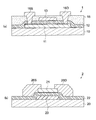
- FIG. 2 is a schematic sectional view of a thin film transistor having an Al alloy film according to the embodiment.
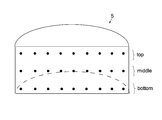
- FIG. 9 is a conceptual diagram illustrating observation points of composition analysis of an Al alloy ingot illustrated in Table 4.
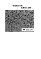
- 6 is an optical microscope image of the aluminum alloy ingot shown in Table 5. It is an electron microscope image of the aluminum alloy ingot concerning this embodiment.
- FIGS. 1A and 1B are schematic cross-sectional views of a thin film transistor having an Al alloy film according to the present embodiment.
- the thin film transistor 1 shown in FIG. 1A is a top gate type thin film transistor.
- an active layer (semiconductor layer) 11, a gate insulating film 12, a gate electrode 13, and a protective layer 15 are stacked on a glass substrate 10.
- the active layer 11 is composed of, for example, LTPS (low temperature poly-silicon).
- the active layer 11 is electrically connected to the source electrode 16S and the drain electrode 16D.
- the thin film transistor 2 shown in FIG. 1B is a bottom gate type thin film transistor.
- a gate electrode 23, a gate insulating film 22, an active layer 21, a source electrode 26S, and a source electrode 26D are stacked on a glass substrate 20.
- the active layer 21 is made of, for example, an IGZO (In-Ga-Zn-O) -based oxide semiconductor material.
- the active layer 21 is electrically connected to the source electrode 26S and the drain electrode 26D.
- the thickness of the gate electrodes 13 and 23 is not particularly limited, and is, for example, 100 nm or more and 600 nm or less, preferably 200 nm or more and 400 nm or less. If the thickness is less than 100 nm, it is difficult to reduce the resistance of the gate electrodes 13 and 23. If the thickness exceeds 600 nm, the bending resistance of the thin film transistor 2 tends to decrease.
- the gate electrodes 13 and 23 are made of the Al alloy film according to the present embodiment.
- the specific resistance of the gate electrodes 13 and 23 (Al alloy film) is set to, for example, 15 ⁇ ⁇ cm or less, preferably 10 ⁇ ⁇ cm or less.
- the gate electrodes 13 and 23 are formed by forming a solid Al alloy film by a sputtering method and then patterning it into a predetermined shape.
- a sputtering method for example, a DC sputtering method, a pulse DC sputtering method, an RF sputtering method, or the like is applied. Either wet etching or dry etching is applied for patterning the solid Al alloy film.
- the film formation and patterning of the gate electrodes 13 and 23 are generally performed during the manufacturing process of the thin film transistors 1 and 2.
- a heat treatment (annealing) is performed as necessary.
- a heat treatment at 550 ° C. or more and 650 ° C. or less for 30 seconds or more and 30 minutes or less may be performed for activation of the active layer 11.
- the gate insulating film 22 may be subjected to heat treatment at 350 ° C. to 450 ° C. for 30 minutes to 180 minutes in order to repair the insulating property.
- a material for the gate electrodes 13 and 23 there is a method of selecting a high melting point metal (for example, Mo) that can endure such a thermal history.
- a high melting point metal for example, Mo
- a gate electrode made of a refractory metal (for example, Mo) as a base material is applied to the curved surface of such a display device, the refractory metal does not have sufficient bending resistance, and thus the refractory metal does not have sufficient bending resistance. Some of the cracks may cause the electrode to break.
- a gate electrode is applied to a curved surface portion of a display device because the gate electrode has a role of forming a channel in an opposing semiconductor layer instead of a wiring for simply passing an electric current, the gate electrode may be cracked or broken. And it is desirable to have excellent bending resistance.
- the gate electrode may have a high resistance or the gate electrode may be disconnected. Further, when another film is formed on the hillock, the film may have a high resistance or be disconnected due to the shape of the underlying hillock.
- the electrode materials constituting the gate electrodes 13 and 23 must have a bending resistance that can withstand a bending radius of 1 mm. It is required to have excellent heat resistance, in which hillocks are hardly generated, and to be able to perform etching without residue.
- an Al alloy film described below is applied as a material for the gate electrodes 13 and 23 in order to address the above problem.
- the Al alloy film according to the present embodiment uses an Al pure metal as a base material, and the Al pure metal includes at least one first additive element selected from the group consisting of Zr, Sc, Mo, Y, Nb, and Ti. It is contained.
- the content of the first additive element is adjusted to, for example, 0.01 atomic% or more and 1.0 atomic% or less, and preferably, 0.1 atomic% or more and 0.5 atomic% or less. Has been adjusted.
- Such an Al alloy film has excellent bending resistance and exhibits the effect of the addition of the first additive element.
- the Orowan stress due to the intermetallic compound acts as a barrier to dislocation line movement in the Al alloy, and even if the Al alloy film is subjected to heat treatment, plastic deformation of the Al alloy film is suppressed. As a result, hillocks hardly occur in the Al alloy film, and an Al alloy film having high heat resistance is formed.
- the gate electrodes 13 and 23 and other wiring films may have electrical defects.
- the above Al alloy film is applied to the gate electrodes 13 and 23, and a highly reliable display device can be provided.
- the content of the first additive element when the content of the first additive element is less than 0.01 atomic%, when the heat treatment is performed on the Al alloy film, the concentration of the intermetallic compound in the Al alloy film is low, and the hillock is contained in the Al alloy film. Is more likely to occur. That is, the heat resistance of the Al alloy film decreases, which is not preferable.
- the content of the first additive element when the content of the first additive element is more than 1.0 atomic%, the heat resistance is maintained, but the bending resistance of the Al alloy film is deteriorated and the specific resistance of the Al alloy film is increased. Absent.
- both wet etching and dry etching can be performed.
- Al pure metal contains at least one kind of second additive element selected from the group of Mn, Si, Cu, Ge, Mg, Ag and Ni. May be done.
- the content of the second additive element in the Al alloy film is adjusted to, for example, 0.2 to 3.0 atomic%, preferably 0.5 to 1.5 atomic%. Has been adjusted.
- the effect of the addition of the second additive element is that even if a heat treatment is performed on the Al alloy film, the second additive element is favorably dissolved in Al and the plastic deformation of the Al alloy film is suppressed.
- Al and the second additive element form an intermetallic compound in the Al alloy film. As a result, hillocks hardly occur in the Al alloy film, and an Al alloy film having high heat resistance is formed.
- the content of the second additive element is less than 0.2 atomic%, when the heat treatment is performed on the Al alloy film, the concentration of the second additive element (solid solution strengthening element) in the Al alloy film And hillocks are easily generated in the Al alloy film. That is, the heat resistance of the Al alloy film decreases, which is not preferable.
- the content of the second additive element is larger than 3.0 atomic%, the heat resistance is maintained, but the bending resistance of the Al alloy film is deteriorated and the specific resistance of the Al alloy film is increased. Absent.
- both wet etching and dry etching can be performed.
- the first and second additive elements may be added to the Al pure metal.
- the Al alloy film contains at least one first additive element selected from the group consisting of Zr, Sc, Mo, Y, Nb, and Ti in Al pure metal, and further contains Mn, Si, Cu,
- a film containing at least one second additive element selected from the group consisting of Ge, Mg, Ag and Ni may be used.
- the content of the first additive element in the Al alloy film is adjusted to, for example, 0.01 to 1.0 atomic%, preferably 0.1 to 0.5 atomic%.
- the content of the second additive element is adjusted to, for example, 0.2 atomic% or more and 3.0 atomic% or less, and preferably adjusted to 0.5 atomic% or more and 1.5 atomic% or less. I have.
- the intermetallic compound may not be sufficiently dispersed and formed. Even in such a case, since the Al alloy film already contains the second additive element (solid solution strengthening element), the Al alloy film is already in a state where hillocks are not easily formed.
- the Al alloy film is subjected to heat treatment and once the intermetallic compound is dispersed and formed in the Al alloy film, it is assumed that stress is generated in the Al alloy film due to agglomerates of Al and the second additive element. Also, the movement of dislocation lines is suppressed by the intermetallic compound of Al and the first additive element. For this reason, a hillock is not easily formed in the Al alloy.
- the Al alloy film contains at least one first additive element selected from the group consisting of Zr, Sc, Mo, Y, Nb, and Ti in an Al pure metal, and further includes Ce, Nd, La, And a film containing at least one third additive element selected from the group of Gd.
- the content of the first additive element in the Al alloy film is adjusted to, for example, 0.01 to 1.0 atomic%, preferably 0.1 to 0.5 atomic%.
- the content of the third additive element is adjusted to, for example, 0.1 atomic% or more and 1.0 atomic% or less, and preferably adjusted to 0.2 atomic% or more and 0.7 atomic% or less. I have.
- the function of the first additional element is further promoted by adding the third additional element to the Al alloy containing the first additional element.
- the third additive element is added to the Al alloy, the intermetallic compound of Al and the first additive element is more uniformly dispersed in the Al alloy.
- the third additive element has a property of precipitating toward grain boundaries when subjected to heat treatment.
- the phenomenon that the grain boundaries serve as barriers and adjacent microcrystals are connected and the crystals are coarsened is suppressed.
- stress is hardly generated in the Al alloy film, and the heat resistance of the Al alloy film is further improved.
- the content of the third additive element is less than 0.1 atomic%, the heat resistance of the Al alloy film decreases, which is not preferable.
- the content of the third additive element is larger than 1.0 atomic%, residues are easily generated when wet etching or dry etching is performed on the Al alloy film, which is not preferable.
- the Al alloy film contains at least one second additive element selected from the group consisting of Mn, Si, Cu, Ge, Mg, Ag, and Ni in Al pure metal, and further includes Ce, Nd, and La. And a film containing at least one third additive element selected from the group of Gd.
- the content of the second additive element in the Al alloy film is adjusted to, for example, 0.2 to 3.0 atomic%, preferably 0.5 to 1.5 atomic%.
- the content of the third additive element is adjusted to, for example, 0.1 atomic% or more and 1.0 atomic% or less, and preferably adjusted to 0.2 atomic% or more and 0.7 atomic% or less. I have.
- the function of the second additive element is further promoted.
- the third additive element is added to the Al alloy, the second additive element is more uniformly dispersed in the Al alloy.
- the third additive element is directed to the grain boundary by the heat treatment, in the Al alloy film, the phenomenon that adjacent fine particles are connected and the fine particles are coarsened is suppressed. As a result, stress is hardly generated in the Al alloy film, and the heat resistance of the Al alloy film is further improved.
- the Al alloy film contains at least one first additive element selected from the group consisting of Zr, Sc, Mo, Y, Nb, and Ti in Al pure metal, and further contains Mn, Si, Cu, At least one second additive element selected from the group consisting of Ge, Mg, Ag and Ni is contained, and at least one third additive element selected from the group consisting of Ce, Nd, La, and Gd is contained.
- a contained film may be used.
- the content of the first additive element in the Al alloy film is adjusted to, for example, 0.01 to 1.0 atomic%, preferably 0.1 to 0.5 atomic%.
- the content of the second additive element is adjusted to, for example, 0.2 atomic% or more and 3.0 atomic% or less, and preferably adjusted to 0.5 atomic% or more and 1.5 atomic% or less
- the content of the third additional element is adjusted to, for example, 0.1 atomic% or more and 1.0 atomic% or less, and preferably adjusted to 0.2 atomic% or more and 0.7 atomic% or less.
- Such an Al alloy film has excellent bending resistance, and the effect of the addition of the first addition element, the effect of the addition of the second addition element, and the effect of the addition of the third addition element are synergistic. It is exhibited in.
- the gate electrodes 13 and 23 made of the Al alloy film are formed, for example, by sputtering in a vacuum chamber.
- a sputtering target used for sputtering film formation an aluminum alloy target (Al alloy target) for forming the gate electrodes 13 and 23 of the thin film transistors 1 and 2 is used.
- a target having the same composition as the Al alloy film is prepared.
- a pure metal piece having a purity of 5N (99.999%) or more is formed by adding a metal piece, a metal powder, or the like of at least one of the first, second, and third additional elements. After being mixed, these mixed materials are easily prepared in a crucible by a melting method such as induction heating.
- the temperature difference between the solidus line and the liquidus line in the phase diagram of the metal compound is obtained by setting the addition amount of at least one of the first additional element, the second additional element, and the third additional element in the above range.
- an Al alloy ingot in which primary crystals of intermetallic compounds or the like are unlikely to settle in the crucible is formed. That is, in the Al alloy ingot, at least one of the first, second, and third additional elements is uniformly dispersed.
- the Al alloy ingot is subjected to plastic processing such as forging, rolling, and pressing, and the Al alloy ingot is processed into a plate shape or a disk shape, thereby producing an Al alloy target.
- the Al alloy target uses an Al pure metal as a base material, and the Al pure metal contains at least one first additive element selected from the group consisting of Zr, Sc, Mo, Y, Nb, and Ti. ing.
- the content of the first additional element is adjusted to, for example, 0.01 to 1.0 atomic%, preferably 0.1 to 0.5 atomic%. Has been adjusted.
- the Al alloy target contains, in place of the first additional element, at least one type of second additional element selected from the group consisting of Mn, Si, Cu, Ge, Mg, Ag, and Ni in Al pure metal. May be done.
- the content of the second additional element is adjusted to, for example, 0.2 to 3.0 atomic%, preferably 0.5 to 1.5 atomic%. Has been adjusted.
- the first additive element and the second additive element may be added to the Al alloy metal in the Al alloy target.
- the Al alloy target contains at least one first additive element selected from the group consisting of Zr, Sc, Mo, Y, Nb, and Ti in Al pure metal, and further contains Mn, Si, Cu, At least one second additive element selected from the group consisting of Ge, Mg, Ag and Ni may be contained.
- the content of the first additive element is adjusted to, for example, 0.01 atomic% or more and 1.0 atomic% or less, preferably, 0.1 atomic% or more and 0.5 atomic% or less.
- the content of the second additive element is adjusted to, for example, 0.2 atomic% or more and 3.0 atomic% or less, and preferably adjusted to 0.5 atomic% or more and 1.5 atomic% or less. I have.
- the Al alloy target contains at least one first additive element selected from the group consisting of Zr, Sc, Mo, Y, Nb, and Ti in pure Al metal, and further includes Ce, Nd, and La. , And at least one third additive element selected from the group of Gd.
- the content of the first additive element is adjusted to, for example, 0.01 atomic% or more and 1.0 atomic% or less, preferably, 0.1 atomic% or more and 0.5 atomic% or less.
- the content of the third additive element is adjusted to, for example, 0.1 atomic% or more and 1.0 atomic% or less, and preferably adjusted to 0.2 atomic% or more and 0.7 atomic% or less. I have.
- the Al alloy target contains at least one second additive element selected from the group consisting of Mn, Si, Cu, Ge, Mg, Ag and Ni in Al pure metal, and further contains Ce, Nd, At least one third additive element selected from the group consisting of La and Gd may be contained.
- the content of the second additional element is adjusted to, for example, 0.2 to 3.0 atomic%, preferably 0.5 to 1.5 atomic%.
- the content of the third additive element is adjusted to, for example, 0.1 atomic% or more and 1.0 atomic% or less, and preferably adjusted to 0.2 atomic% or more and 0.7 atomic% or less. I have.
- the Al alloy target contains at least one first additive element selected from the group consisting of Zr, Sc, Mo, Y, Nb, and Ti in Al pure metal, and further includes Mn, Si, and Cu. , Ge, Mg, Ag, and Ni, and at least one third additive element selected from the group consisting of Ce, Nd, La, and Gd. May be contained.
- the content of the first additive element is adjusted to, for example, 0.01 atomic% or more and 1.0 atomic% or less, preferably, 0.1 atomic% or more and 0.5 atomic% or less.
- the content of the second additive element is adjusted to, for example, 0.2 atomic% or more and 3.0 atomic% or less, and preferably adjusted to 0.5 atomic% or more and 1.5 atomic% or less
- the content of the third additional element is adjusted to, for example, 0.1 atomic% or more and 1.0 atomic% or less, and preferably adjusted to 0.2 atomic% or more and 0.7 atomic% or less.
- Al alloy film formed by sputtering using such an Al alloy target exhibits the above-described excellent effects.
- the Al ingot receives heat during plastic working such as forging, rolling, and pressing, and Al crystal grains may grow in the Al ingot.
- Al crystal grains also exist in the Al target manufactured from such an Al ingot, and during the film formation, the Al crystal grains receive heat from the plasma to form protrusions on the surface of the Al target. These projections may cause abnormal discharge, or the projections may jump out of the Al target during film formation.
- the Al alloy target of the present embodiment at least one of the first, second, and third additional elements is added to the Al pure metal in the above-described amount.
- the content of at least one of Ce, Mn, and Si in the grain boundary between the particles is increased. Is higher than at least one of Ce, Mn, and Si.
- the average particle size of the particles is adjusted to 10 ⁇ m or more and 100 ⁇ m or less. The average particle size is determined by a laser diffraction method, image analysis using an electron microscope image, or the like.
- the grain boundary serves as a barrier, and the phenomenon that the adjacent fine particles are connected and the fine particles are coarsened is suppressed.
- the heat resistance of the Al alloy target is further improved.
- the sputtering conditions for the Al alloy film are as follows. Discharge method: DC discharge Film formation temperature: room temperature (25 ° C) Film forming pressure: 0.3 Pa Film thickness: 200 nm
- the heat treatment of the Al alloy film is performed in a nitrogen atmosphere at 400 ° C. for 1 hour and further at 600 ° C. for 2 minutes.
- Table 1 shows an example of the bending characteristics of the Mo film, the Al film, and the Al alloy film.
- the unit of the concentration is atomic% (at%).
- a two-layered SiN film (200 nm) / polyimide layer (25 ⁇ m) substrate was used.
- each of the Mo film, the Al film, and the Al alloy film is formed by sputtering on the SiN film.
- the bending radius in the bending test is 1 mm.
- the test speed is 30 rpm.
- the bending was performed in the order of once, 1,000 times, 10,000 times, and 100,000 times. The presence or absence of cracks was visually determined from the image of the optical microscope.
- Table 2 shows an example of the specific resistance ( ⁇ ⁇ cm) and the surface roughness (nm) of the Al film and the Al alloy film.
- the specific resistance of the Al alloy film becomes 10 ⁇ ⁇ cm or less. It turns out that it becomes. It is also found that the specific resistance of the Al alloy film becomes 10 ⁇ ⁇ cm or less even when the second pure element of Mn and Si is contained in the Al pure metal at 0.2 at% or more and 3.0 at% or less. .
- the surface roughness is measured by AFM (Atomic Force Microscopy). The surface roughness was observed immediately after film formation (As @ Depo.), After one hour at 400 ° C., and after two minutes at 600 ° C. The measurement range is 5 ⁇ m square.
- the upper row of each column shows the Rq value (nm), and the lower row shows the PV value (nm).
- the Rq value is the root mean square height
- the PV value is the difference between the maximum height (peak) and the minimum height (valley).
- the PV value tends to increase.
- the PV value of the wiring film is preferably smaller, and more preferably, 50 nm or less. In particular, by applying an Al alloy film having a PV value of 50 nm or less to the bent portion of the display panel, even if the Al alloy film is bent, the adhesion with the upper layer of the Al alloy film is improved.
- the Al film and the Al alloy film both have a surface roughness of 50 nm or less.
- the PV value of the Al film exceeds 300 nm.
- the PV value of the Al alloy film is smaller than that of the Al film. That is, it can be determined that hillocks are less likely to grow in the Al alloy film than in the Al film even after the heat treatment.
- Table 3 shows an example of the presence or absence of a residue after the etching of the Al film and the Al alloy film.
- an etching gas is a mixed gas of Cl 2 (50 sccm) / Ar (20 sccm).
- the etching pressure is 1.0 Pa.
- the discharge power is 400 W when the substrate bias power is 200 W.
- a mixed solution of phosphoric acid / nitric acid / acetic acid / water (commonly referred to as PAN) is used.
- the liquid temperature is 40 ° C.
- an Al alloy film containing 0.5 at% of Ce as the third additive element (Al-0.5 at% Ce, Al-0.3 at% Sc-0.2 at% Zr-0. 5at% Ce, Al-0.3at% Sc-0.2at% Zr-0.5at% Ce-1.0at% Mn-0.5at% Si) enables dry etching and wet etching without any residue Has become.
- concentration of Ce increased, and in the Al alloy film with 2.0 at% Ce (Al-2.0 at% Ce), residues were generated by dry etching.
- metal materials of Al, Sc, Zr, Mn, Si, and Ce are placed in a crucible.
- each metal is set so that the component ratio of the additive element of the Al alloy target is 0.2 at% Sc, 0.1 at% Zr, 1.0 at% Mn, 0.5 at% Si, and 0.5 at% Ce.
- Materials are placed in the crucible.
- each metal material is heated to a melting temperature (for example, 1050 ° C.) higher than the melting point of the Al alloy (for example, 640 ° C.) by 400 ° C., and each metal material is melted in the crucible. You. Next, from this melting temperature, the molten metal is cooled to room temperature to form an aluminum alloy ingot. Thereafter, the aluminum alloy ingot is forged as necessary, and the aluminum alloy ingot is cut into a plate shape or a disk shape. Thereby, an Al alloy target is formed.
- a melting temperature for example, 1050 ° C.
- the melting point of the Al alloy for example, 640 ° C.
- a metal material is melted at a melting temperature slightly higher than the melting point of the metal material, and the metal material is cooled from the slightly higher melting temperature to form an alloy ingot.
- the melting temperature is set to a temperature slightly higher than the melting point, the metal material may not be sufficiently mixed.
- the metal materials are heated and melted at a melting temperature higher than the melting point of the Al alloy by 400 ° C. or more, the respective metal materials are sufficiently mixed.
- the higher the melting temperature the longer the cooling time from the melting temperature to room temperature, and the more easily the intermetallic compound is precipitated.
- the intermetallic compound is hardly precipitated in the Al alloy ingot. The element concentration has been adjusted.
- FIG. 2 is a conceptual diagram illustrating observation points in the composition analysis of the Al alloy ingot exemplified in Table 4.
- Table 4 shows an example of the concentration distribution of each element contained in the Al alloy ingot.
- FIG. 2 illustrates, for example, a semi-cylindrical Al alloy ingot 5 obtained by dividing a cylindrical Al alloy ingot (100 mm diameter ⁇ 50 mmt) into two.
- Table 4 shows the average concentration (at%) measured from the nine observation points of each element at the top position and the average value measured from the nine observation points of each element at the middle position. The concentration (at%) and the average concentration (at%) measured from nine observation points of each element at the bottom position are shown. Table 4 also shows the deviation of the average value of the concentration ⁇ 3 ⁇ .
- the composition ratio of the additive elements of the Al alloy ingot was such that Sc was 0.2 at%, Zr was 0.1 at%, and Mn was 1.0 at% at any position of top, middle, and bottom.
- Si is about 0.5 at% and Ce is about 0.5 at%, and it can be seen that in the Al alloy ingot, the respective metal materials are uniformly dispersed in the longitudinal direction and the lateral direction of the Al alloy ingot.
- Table 5 shows the Zr concentration distribution of the aluminum alloy ingot when Sc was added at 0.2 at% and Zr was added at 3.5 at%.
- the manufacturing method is the same as the aluminum alloy ingot shown in Table 4.
- Table 5 when the Zr concentration was increased to 3.5 at%, it was found that the Zr concentration increased from the top to the bottom of the aluminum alloy ingot. An electron microscope image in this case is shown in FIG.
- FIG. 3 is an optical microscope image of the aluminum alloy ingot shown in Table 5.
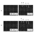
- FIGS. 4A and 4B are electron microscope images of the aluminum alloy ingot according to the present embodiment.
- FIG. 4A shows a surface electron microscope image of the aluminum alloy ingot shown in Table 4.
- FIG. 4B shows a surface electron microscope image of the aluminum alloy ingot shown in Table 4 after heat treatment at 600 ° C. for 2 hours.
- the right images in FIGS. 4A and 4B are images obtained by enlarging the scale of the left image.
- the aluminum alloy ingot was composed of a group of particles A having an average particle diameter of about 10 ⁇ m.
- Ce, Mn, and Si were observed at a high concentration at the grain boundary B. That is, it is found that the content of at least one of Ce, Mn, and Si in the grain boundary between the particles A is higher than the content of at least one of Ce, Mn, and Si in the particle A.
- FIG. 4 (b) shows an image obtained by performing a heat treatment at 600 ° C. for 2 hours from the state shown in FIG. 4 (a).
- the particle size is limited to about 10 ⁇ m, and the particles A do not combine with each other to grow into a giant particle, and no new particles (for example, an intermetallic compound) are precipitated in the particle A. .
- the Al alloy film is applied to the gate electrodes 13 and 23 has been described, but the Al alloy film is applied to the source / drain electrodes, other electrodes other than the source / drain electrodes, or the wiring. It is also possible.
Landscapes
- Chemical & Material Sciences (AREA)
- Engineering & Computer Science (AREA)
- Materials Engineering (AREA)
- Mechanical Engineering (AREA)
- Metallurgy (AREA)
- Organic Chemistry (AREA)
- Chemical Kinetics & Catalysis (AREA)
- Thermal Sciences (AREA)
- Crystallography & Structural Chemistry (AREA)
- Physics & Mathematics (AREA)
- Electrodes Of Semiconductors (AREA)
- Thin Film Transistor (AREA)
- Composite Materials (AREA)
- Physical Vapour Deposition (AREA)
Abstract
Description
本発明は、アルミニウム合金膜、その製造方法、及びアルミニウム合金膜を備えた薄膜トランジスタに関する。 The present invention relates to an aluminum alloy film, a method for manufacturing the same, and a thin film transistor provided with the aluminum alloy film.
液晶表示素子、有機EL表示素子等の薄膜トランジスタ(TFT)では、例えば、Al配線が低抵抗配線材料として使用されることがある。 薄膜 ト ラ ン ジ ス タ In a thin film transistor (TFT) such as a liquid crystal display element or an organic EL display element, for example, an Al wiring may be used as a low-resistance wiring material.
しかし、配線の中でもゲート電極は、一般的に製造工程の途中で形成されることから、ゲート電極形成後にアニール処理による熱履歴を受けることになる。このため、ゲート電極の材料としては、熱履歴に耐え得る高融点金属(例えば、Mo)が使用されることが多い(例えば、特許文献1参照)。 However, since the gate electrode among the wirings is generally formed during the manufacturing process, it receives a heat history due to the annealing process after the gate electrode is formed. For this reason, a high melting point metal (for example, Mo) that can withstand heat history is often used as a material for the gate electrode (for example, see Patent Document 1).
しかしながら、Moといった高融点金属を曲面形状の画面を持ったディスプレイや、折り曲げ可能なフォルダブルディスプレイの曲面部の電極に適用した場合、高融点金属が充分な屈曲耐性を持っていないことから、電極が屈曲によって破断する可能性がある。 However, when a refractory metal such as Mo is applied to a display having a curved screen or an electrode on a curved portion of a foldable display, the refractory metal does not have sufficient bending resistance. May be broken by bending.
また、高融点金属に代えて、屈曲性に優れた電極材に採用した場合には、電極が熱履歴に対して充分な耐性を備えている必要がある。 (4) When an electrode material having excellent flexibility is used instead of the high melting point metal, the electrode needs to have sufficient resistance to heat history.
以上のような事情に鑑み、本発明の目的は、屈曲耐性及び耐熱性に優れたアルミニウム合金膜、及び、該アルミニウム合金膜を備えた薄膜トランジスタを提供することにある。 In view of the circumstances described above, an object of the present invention is to provide an aluminum alloy film having excellent bending resistance and heat resistance, and a thin film transistor provided with the aluminum alloy film.
上記目的を達成するため、本発明の一形態に係るアルミニウム合金膜は、Al純金属に、Zr、Sc、Mo、Y、Nb、及びTiの群から選択される少なくとも1種の第1添加元素が含有されている。
上記第1添加元素の含有量が0.01原子%以上1.0原子%以下である。
このようなアルミニウム合金膜であれば、アルミニウム合金膜が優れた屈曲耐性を有し、優れた耐熱性を有する。また、アルミニウム合金膜は、エッチングも可能になる。
In order to achieve the above object, an aluminum alloy film according to one embodiment of the present invention is a method in which an Al pure metal is formed by adding at least one first additive element selected from the group consisting of Zr, Sc, Mo, Y, Nb, and Ti. Is contained.
The content of the first additive element is 0.01 atomic% or more and 1.0 atomic% or less.
With such an aluminum alloy film, the aluminum alloy film has excellent bending resistance and excellent heat resistance. Further, the aluminum alloy film can be etched.
上記のアルミニウム合金膜においては、さらに、Mn、Si、Cu、Ge、Mg、Ag及びNiの群から選択される少なくとも1種の第2添加元素が含有され、上記第2添加元素の含有量が0.2原子%以上3.0原子%以下でもよい。
このようなアルミニウム合金膜であれば、アルミニウム合金膜が優れた屈曲耐性を有し、さらに、優れた耐熱性を有する。また、アルミニウム合金膜は、エッチングも可能になる。
The above-mentioned aluminum alloy film further contains at least one second additive element selected from the group consisting of Mn, Si, Cu, Ge, Mg, Ag, and Ni, and the content of the second additive element is reduced. It may be 0.2 atomic% or more and 3.0 atomic% or less.
With such an aluminum alloy film, the aluminum alloy film has excellent bending resistance and further has excellent heat resistance. Further, the aluminum alloy film can be etched.
上記目的を達成するため、本発明の一形態に係るアルミニウム合金膜は、Al純金属に、Mn、Si、Cu、Ge、Mg、Ag及びNiの群から選択される少なくとも1種の第2添加元素が含有されている。
上記第2添加元素の含有量は、0.2原子%以上3.0原子%以下でもよい。
このようなアルミニウム合金膜であれば、アルミニウム合金膜が優れた屈曲耐性を有し、さらに、優れた耐熱性を有する。また、アルミニウム合金膜は、エッチングも可能になる。
In order to achieve the above object, an aluminum alloy film according to one embodiment of the present invention is a method in which at least one kind of second addition selected from the group consisting of Mn, Si, Cu, Ge, Mg, Ag, and Ni is added to Al pure metal. Contains elements.
The content of the second additive element may be not less than 0.2 atomic% and not more than 3.0 atomic%.
With such an aluminum alloy film, the aluminum alloy film has excellent bending resistance and further has excellent heat resistance. Further, the aluminum alloy film can be etched.
上記のアルミニウム合金膜においては、さらに、Ce、Nd、La、及びGdの群から選択される少なくとも1種の第3添加元素が含有され、上記第3添加元素の含有量が0.1原子%以上1.0原子%以下でもよい。
このようなアルミニウム合金膜であれば、アルミニウム合金膜が優れた屈曲耐性を有し、粒界に第3添加元素が析出することで優れた耐熱性を有する。また、また、アルミニウム合金膜は、エッチングも可能になる。
The above aluminum alloy film further contains at least one third additive element selected from the group consisting of Ce, Nd, La, and Gd, and the content of the third additive element is 0.1 atomic%. It may be not less than 1.0 atomic%.
With such an aluminum alloy film, the aluminum alloy film has excellent bending resistance, and has excellent heat resistance due to precipitation of the third additive element at the grain boundary. Further, the aluminum alloy film can be etched.
上記のアルミニウム合金膜においては、屈曲半径1mmに折り曲げられた場合に耐え得る屈曲耐性を有してもよい。 The above-mentioned aluminum alloy film may have a bending resistance that can withstand a bending radius of 1 mm.
上記のアルミニウム合金膜においては、ドライエッチング及びウェットエッチングが可能であってもよい。 ド ラ イ In the above aluminum alloy film, dry etching and wet etching may be possible.
上記のアルミニウム合金膜においては、表面粗さP-V値が50nm以下であってもよい。 表面 In the above aluminum alloy film, the surface roughness PV value may be 50 nm or less.
上記のアルミニウム合金膜においては、比抵抗が10μΩ・cm以下であってもよい。 比 In the above aluminum alloy film, the specific resistance may be 10 μΩ · cm or less.
上記目的を達成するため、本発明の一形態に係る薄膜トランジスタは、上記のアルミニウム合金膜で構成されたゲート電極を具備する。 た め In order to achieve the above object, a thin film transistor according to one embodiment of the present invention includes a gate electrode formed of the above aluminum alloy film.
また、上記目的を達成するため、本発明の一形態では、上記のアルミニウム合金膜の製造方法が提供される。 According to another embodiment of the present invention, there is provided a method for manufacturing the above-described aluminum alloy film.
以上述べたように、本発明によれば、屈曲耐性及び耐熱性に優れたアルミニウム合金膜、その製造方法及び、該アルミニウム合金膜を備えた薄膜トランジスタが提供される。 As described above, according to the present invention, an aluminum alloy film having excellent bending resistance and heat resistance, a method for manufacturing the same, and a thin film transistor provided with the aluminum alloy film are provided.
以下、図面を参照しながら、本発明の実施形態を説明する。各図面には、XYZ軸座標が導入される場合がある。また、同一の部材または同一の機能を有する部材には同一の符号を付し、その部材を説明した後には適宜説明を省略する場合がある。 Hereinafter, embodiments of the present invention will be described with reference to the drawings. In each drawing, XYZ axis coordinates may be introduced. In addition, the same members or members having the same functions are denoted by the same reference numerals, and after the members are described, the description may be appropriately omitted.
(薄膜トランジスタ) (Thin film transistor)
図1(a)及び図1(b)は、本実施形態に係るAl合金膜を有する薄膜トランジスタの概略断面図である。 FIGS. 1A and 1B are schematic cross-sectional views of a thin film transistor having an Al alloy film according to the present embodiment.
図1(a)に示す薄膜トランジスタ1は、トップゲート型の薄膜トランジスタである。薄膜トランジスタ1では、ガラス基板10上に、活性層(半導体層)11、ゲート絶縁膜12、ゲート電極13、及び保護層15が積層されている。活性層11は、例えば、LTPS(low temperature poly-silicon)で構成される。活性層11は、ソース電極16S及びドレイン電極16Dに電気的に接続されている。
薄膜 ト ラ ン ジ ス タ The thin
図1(b)に示す薄膜トランジスタ2は、ボトムゲート型の薄膜トランジスタである。薄膜トランジスタ2では、ガラス基板20上に、ゲート電極23、ゲート絶縁膜22、活性層21、ソース電極26S、及びソース電極26Dが積層されている。活性層21は、例えば、IGZO(In-Ga-Zn-O)系酸化物半導体材料で構成される。活性層21は、ソース電極26S及びドレイン電極26Dに電気的に接続されている。
薄膜 ト ラ ン ジ ス タ The thin
ゲート電極13、23の厚みは、特に限定されず、例えば、100nm以上600nm以下、好ましくは、200nm以上400nm以下である。100nm未満の厚みではゲート電極13、23の低抵抗化が困難になる。600nmを超える厚みでは、薄膜トランジスタ2の屈曲耐性が低下する傾向にある。ゲート電極13、23は、本実施形態に係るAl合金膜で構成される。ゲート電極13、23(Al合金膜)の比抵抗は、例えば、15μΩ・cm以下、好ましくは、10μΩ・cm以下に設定されている。
The thickness of the
ゲート電極13、23は、ベタ状のAl合金膜がスパッタリング法で成膜された後、所定形状にパターニングされることで形成される。スパッタリング法は、例えば、DCスパッタリング法、パルスDCスパッタリング法、RFスパッタリング法等が適用される。ベタ状のAl合金膜のパターニングには、ウェットエッチング、ドライエッチングのいずれかが適用される。ゲート電極13、23の成膜及びパターニングは、一般的に薄膜トランジスタ1、2の製造工程の途中で行われる。
The
例えば、薄膜トランジスタ1、2の製造工程では、必要に応じて加熱処理(アニール)が施される。例えば、活性層11の活性化のために、550℃以上650℃以下で、30秒以上30分以下の加熱処理がなされる場合がある。また、ゲート絶縁膜22においては、絶縁性の補修のために、350℃以上450℃以下で、30分以上180分以下の加熱処理がなされる場合がある。
For example, in the manufacturing process of the
従って、ゲート電極13、23の材料としては、このような熱履歴に耐え得る高融点金属(例えば、Mo)を選択する手法もある。
Therefore, as a material for the
しかし、近年では、薄膜トランジスタ1、2がフラット型の表示デバイスだけでなく、周縁部が湾曲したカーブ(Curved)型の表示デバイス、円弧状に折り曲げられたベンダブル(Bendable)型の表示デバイス、180度折り畳み可能なフォルダブル(Foldable)型の表示デバイス等に適用される場合がある。
However, in recent years, not only display devices in which the
このような表示デバイスの曲面部に、高融点金属(例えば、Mo)がベース材料となったゲート電極が適用されると、高融点金属が充分な屈曲耐性を持っていないことから、ゲート電極の一部が亀裂して、該電極が破断する可能性がある。特に、ゲート電極は、単に電流を流す配線ではなく、対向する半導体層にチャネルを形成する役割を有することから表示デバイスの曲面部にゲート電極が適用された場合、ゲート電極は、亀裂、破断がなく、優れた屈曲耐性を備えていることが望ましい。 When a gate electrode made of a refractory metal (for example, Mo) as a base material is applied to the curved surface of such a display device, the refractory metal does not have sufficient bending resistance, and thus the refractory metal does not have sufficient bending resistance. Some of the cracks may cause the electrode to break. In particular, when a gate electrode is applied to a curved surface portion of a display device because the gate electrode has a role of forming a channel in an opposing semiconductor layer instead of a wiring for simply passing an electric current, the gate electrode may be cracked or broken. And it is desirable to have excellent bending resistance.
これに対処するために、柔軟性に優れたAl純金属をゲート電極の材料に適用する方法がある。しかし、Al純金属でゲート電極を構成すると、加熱処理の履歴によってAlの結晶粒径が大径化し、ゲート電極内に応力(圧縮応力、引張応力)が発生して、電極表面にヒロックが発生する場合がある。 (4) In order to cope with this, there is a method of applying Al pure metal having excellent flexibility to the gate electrode material. However, when the gate electrode is composed of pure Al metal, the crystal grain size of Al increases due to the history of the heat treatment, and stress (compression stress, tensile stress) is generated in the gate electrode, and hillocks are generated on the electrode surface. May be.
このようなヒロックがゲート電極から剥離すると、ゲート電極が高抵抗になったり、ゲート電極が断線したりする可能性がある。さらに、ヒロック上に別の膜が形成された場合には、この膜が下地のヒロックの形状を受けて、高抵抗になったり、膜が断線したりする可能性がある。 す る と If such hillocks are separated from the gate electrode, the gate electrode may have a high resistance or the gate electrode may be disconnected. Further, when another film is formed on the hillock, the film may have a high resistance or be disconnected due to the shape of the underlying hillock.
また、ゲート電極13、23のパターニングでは、ウェットエッチング及びドライエッチングのいずれかが適用されるため、ゲート電極13、23においては、ウェットエッチング及びドライエッチングで残渣なく加工されることが要求される。
In addition, in the patterning of the
このように、ゲート電極13、23を構成する電極材としては、ゲート電極13、23が低抵抗であることは基より、屈曲半径1mmに折り曲げられても耐え得る屈曲耐性を有していること、ヒロックが発生しにくい優れた耐熱性を有していること、残渣なくエッチング加工ができることが要求される。
As described above, since the
(Al合金膜) (Al alloy film)
本実施形態では、上記の課題に対処するために、ゲート電極13、23の材料として、以下に説明するAl合金膜が適用される。
In the present embodiment, an Al alloy film described below is applied as a material for the
本実施形態に係るAl合金膜は、Al純金属をベース材料とし、Al純金属に、Zr、Sc、Mo、Y、Nb、及びTiの群から選択される少なくとも1種の第1添加元素が含有されている。ここで、Al合金膜において、第1添加元素の含有量は、例えば、0.01原子%以上1.0原子%以下に調整され、好ましくは、0.1原子%以上0.5原子%以下に調整されている。 The Al alloy film according to the present embodiment uses an Al pure metal as a base material, and the Al pure metal includes at least one first additive element selected from the group consisting of Zr, Sc, Mo, Y, Nb, and Ti. It is contained. Here, in the Al alloy film, the content of the first additive element is adjusted to, for example, 0.01 atomic% or more and 1.0 atomic% or less, and preferably, 0.1 atomic% or more and 0.5 atomic% or less. Has been adjusted.
このようなAl合金膜であれば、優れた屈曲耐性を有するとともに、第1添加元素の添加による効果が発揮される。 で あ れ ば Such an Al alloy film has excellent bending resistance and exhibits the effect of the addition of the first additive element.
例えば、第1添加元素の添加による作用として、Al合金膜に加熱処理がなされたとしても、Alと第1添加元素とによる微小な金属間化合物(平均粒径:1μm以下)がAl合金内で分散形成されることがあげられる。これにより、例えば、金属間化合物によるオロワン応力がAl合金における転位線移動の障壁として働き、Al合金膜に加熱処理が施されても、Al合金膜の塑性変形が抑制される。この結果、Al合金膜には、ヒロックが発生しにくくなり、耐熱性の高いAl合金膜が形成される。 For example, as a function of the addition of the first additive element, even if a heat treatment is performed on the Al alloy film, a minute intermetallic compound (average particle diameter: 1 μm or less) due to Al and the first additive element is formed in the Al alloy. And dispersion forming. Thus, for example, the Orowan stress due to the intermetallic compound acts as a barrier to dislocation line movement in the Al alloy, and even if the Al alloy film is subjected to heat treatment, plastic deformation of the Al alloy film is suppressed. As a result, hillocks hardly occur in the Al alloy film, and an Al alloy film having high heat resistance is formed.
特に、表示デバイスの製造中に、ゲート電極13、23にヒロックが発生すると、ゲート電極13、23、他の配線膜の電気的不良が生じる可能性がある。本実施形態では、上記のAl合金膜をゲート電極13、23に適用し、信頼性の高い表示デバイスを提供することができる。
Especially, if hillocks occur in the
ここで、第1添加元素の含有量が0.01原子%より小さいと、Al合金膜に加熱処理が施された場合、Al合金膜内の金属間化合物の濃度が低く、Al合金膜にヒロックが発生しやすくなる。すなわち、Al合金膜の耐熱性が低下し、好ましくない。一方、第1添加元素の含有量が1.0原子%より大きいと、耐熱性は維持されるものの、Al合金膜の屈曲耐性が悪くなるととともに、Al合金膜の比抵抗が増加するので、好ましくない。 Here, when the content of the first additive element is less than 0.01 atomic%, when the heat treatment is performed on the Al alloy film, the concentration of the intermetallic compound in the Al alloy film is low, and the hillock is contained in the Al alloy film. Is more likely to occur. That is, the heat resistance of the Al alloy film decreases, which is not preferable. On the other hand, when the content of the first additive element is more than 1.0 atomic%, the heat resistance is maintained, but the bending resistance of the Al alloy film is deteriorated and the specific resistance of the Al alloy film is increased. Absent.
また、上記の濃度で第1添加元素が含有したAl合金膜であれば、ウェットエッチング、ドライエッチングのいずれも可能になる。 ウ ェ ッ ト Also, if the Al alloy film contains the first additive element at the above concentration, both wet etching and dry etching can be performed.
また、Al合金膜としては、第1添加元素に代えて、Al純金属に、Mn、Si、Cu、Ge、Mg、Ag及びNiの群から選択される少なくとも1種の第2添加元素が含有されてもよい。この場合、Al合金膜において、第2添加元素の含有量は、例えば、0.2原子%以上3.0原子%以下に調整され、好ましくは、0.5原子%以上1.5原子%以下に調整されている。 Further, as the Al alloy film, instead of the first additive element, Al pure metal contains at least one kind of second additive element selected from the group of Mn, Si, Cu, Ge, Mg, Ag and Ni. May be done. In this case, the content of the second additive element in the Al alloy film is adjusted to, for example, 0.2 to 3.0 atomic%, preferably 0.5 to 1.5 atomic%. Has been adjusted.
このようなAl合金膜であれば、優れた屈曲耐性を有するとともに、第2添加元素の添加による効果が発揮される。 で あ れ ば With such an Al alloy film, it has excellent bending resistance and exhibits the effect of the addition of the second additive element.
例えば、第2添加元素の添加による作用として、Al合金膜に加熱処理がなされたとしても、第2添加元素がAlに良好に固溶され、Al合金膜の塑性変形が抑制されることがあげられる。また、Alと第2添加元素とは、Al合金膜内で金属間化合物を形成する場合もある。この結果、Al合金膜には、ヒロックが発生しにくくなり、耐熱性の高いAl合金膜が形成される。 For example, the effect of the addition of the second additive element is that even if a heat treatment is performed on the Al alloy film, the second additive element is favorably dissolved in Al and the plastic deformation of the Al alloy film is suppressed. Can be In some cases, Al and the second additive element form an intermetallic compound in the Al alloy film. As a result, hillocks hardly occur in the Al alloy film, and an Al alloy film having high heat resistance is formed.
ここで、第2添加元素の含有量が0.2原子%より小さいと、Al合金膜に加熱処理が施された場合、Al合金膜内での第2添加元素(固溶強化元素)の濃度が低く、Al合金膜にヒロックが発生しやすくなる。すなわち、Al合金膜の耐熱性が低下し、好ましくない。一方、第2添加元素の含有量が3.0原子%より大きいと、耐熱性は維持されるものの、Al合金膜の屈曲耐性が悪くなるととともに、Al合金膜の比抵抗が増加するので、好ましくない。 Here, when the content of the second additive element is less than 0.2 atomic%, when the heat treatment is performed on the Al alloy film, the concentration of the second additive element (solid solution strengthening element) in the Al alloy film And hillocks are easily generated in the Al alloy film. That is, the heat resistance of the Al alloy film decreases, which is not preferable. On the other hand, when the content of the second additive element is larger than 3.0 atomic%, the heat resistance is maintained, but the bending resistance of the Al alloy film is deteriorated and the specific resistance of the Al alloy film is increased. Absent.
また、上記の濃度で第2添加元素が含有したAl合金膜であれば、ウェットエッチング、ドライエッチングのいずれも可能になる。 ウ ェ ッ ト Also, if the Al alloy film contains the second additive element at the above concentration, both wet etching and dry etching can be performed.
また、Al合金膜においては、第1添加元素及び第2添加元素がAl純金属に添加されてもよい。 In the Al alloy film, the first and second additive elements may be added to the Al pure metal.
例えば、Al合金膜は、Al純金属に、Zr、Sc、Mo、Y、Nb、及びTiの群から選択される少なくとも1種の第1添加元素が含有され、さらに、Mn、Si、Cu、Ge、Mg、Ag及びNiの群から選択される少なくとも1種の第2添加元素が含有された膜でもよい。この場合、Al合金膜において、第1添加元素の含有量は、例えば、0.01原子%以上1.0原子%以下に調整され、好ましくは、0.1原子%以上0.5原子%以下に調整され、第2添加元素の含有量は、例えば、0.2原子%以上3.0原子%以下に調整され、好ましくは、0.5原子%以上1.5原子%以下に調整されている。 For example, the Al alloy film contains at least one first additive element selected from the group consisting of Zr, Sc, Mo, Y, Nb, and Ti in Al pure metal, and further contains Mn, Si, Cu, A film containing at least one second additive element selected from the group consisting of Ge, Mg, Ag and Ni may be used. In this case, the content of the first additive element in the Al alloy film is adjusted to, for example, 0.01 to 1.0 atomic%, preferably 0.1 to 0.5 atomic%. The content of the second additive element is adjusted to, for example, 0.2 atomic% or more and 3.0 atomic% or less, and preferably adjusted to 0.5 atomic% or more and 1.5 atomic% or less. I have.
このようなAl合金膜であれば、優れた屈曲耐性を有するとともに、第1添加元素の添加による効果と、第2添加元素の添加による効果とが相乗的に発揮される。 で あ れ ば With such an Al alloy film, while having excellent bending resistance, the effect of the addition of the first addition element and the effect of the addition of the second addition element are synergistically exhibited.
例えば、加熱処理前のAl合金膜においては、金属間化合物が充分に分散形成されていない場合がある。このような場合でも、Al合金膜には、第2添加元素(固溶強化元素)が既に含有されているため、Al合金膜は、既にヒロックが形成されにくい状態にある。一方、Al合金膜が加熱処理されて、Al合金膜中に一旦、金属間化合物が分散形成されてしまえば、Alと第2添加元素とによる凝集物によってAl合金膜中に応力が発生したとしても、Alと第1添加元素による金属間化合物によって転位線の移動が抑制される。このため、Al合金中にヒロックが形成されにくい。 For example, in the Al alloy film before the heat treatment, the intermetallic compound may not be sufficiently dispersed and formed. Even in such a case, since the Al alloy film already contains the second additive element (solid solution strengthening element), the Al alloy film is already in a state where hillocks are not easily formed. On the other hand, if the Al alloy film is subjected to heat treatment and once the intermetallic compound is dispersed and formed in the Al alloy film, it is assumed that stress is generated in the Al alloy film due to agglomerates of Al and the second additive element. Also, the movement of dislocation lines is suppressed by the intermetallic compound of Al and the first additive element. For this reason, a hillock is not easily formed in the Al alloy.
また、Al合金膜は、Al純金属に、Zr、Sc、Mo、Y、Nb、及びTiの群から選択される少なくとも1種の第1添加元素が含有され、さらに、Ce、Nd、La、及びGdの群から選択される少なくとも1種の第3添加元素が含有された膜でもよい。この場合、Al合金膜において、第1添加元素の含有量は、例えば、0.01原子%以上1.0原子%以下に調整され、好ましくは、0.1原子%以上0.5原子%以下に調整され、第3添加元素の含有量は、例えば、0.1原子%以上1.0原子%以下に調整され、好ましくは、0.2原子%以上0.7原子%以下に調整されている。 The Al alloy film contains at least one first additive element selected from the group consisting of Zr, Sc, Mo, Y, Nb, and Ti in an Al pure metal, and further includes Ce, Nd, La, And a film containing at least one third additive element selected from the group of Gd. In this case, the content of the first additive element in the Al alloy film is adjusted to, for example, 0.01 to 1.0 atomic%, preferably 0.1 to 0.5 atomic%. The content of the third additive element is adjusted to, for example, 0.1 atomic% or more and 1.0 atomic% or less, and preferably adjusted to 0.2 atomic% or more and 0.7 atomic% or less. I have.
このようなAl合金膜であれば、優れた屈曲耐性を有するとともに、第1添加元素の添加による効果と、第3添加元素の添加による効果とが相乗的に発揮される。 (4) With such an Al alloy film, it has excellent bending resistance, and the effect of the addition of the first additive element and the effect of the addition of the third additive element are synergistically exhibited.
例えば、第3添加元素が第1添加元素を含むAl合金に添加されることにより、第1添加元素の機能がより促進する。例えば、第3添加元素がAl合金に添加されると、Alと第1添加元素とによる金属間化合物がAl合金中により均一に分散される。 For example, the function of the first additional element is further promoted by adding the third additional element to the Al alloy containing the first additional element. For example, when the third additive element is added to the Al alloy, the intermetallic compound of Al and the first additive element is more uniformly dispersed in the Al alloy.
さらに、第3添加元素は、加熱処理がなされると、粒界に向かって析出する性質を有する。これにより、Al合金膜においては、粒界が障壁となり、隣接する微結晶が繋がって結晶が粗大化する現象が抑制される。この結果、Al合金膜内には応力が発生しにくくなり、Al合金膜の耐熱性がさらに向上する。 Furthermore, the third additive element has a property of precipitating toward grain boundaries when subjected to heat treatment. As a result, in the Al alloy film, the phenomenon that the grain boundaries serve as barriers and adjacent microcrystals are connected and the crystals are coarsened is suppressed. As a result, stress is hardly generated in the Al alloy film, and the heat resistance of the Al alloy film is further improved.
ここで、第3添加元素の含有量が0.1原子%より小さくなると、Al合金膜の耐熱性が減少し、好ましくない。一方、第3添加元素の含有量が1.0原子%よりも大きくなると、Al合金膜にウェットエッチングまたはドライエッチングを施した場合、残渣が発生しやすく、好ましくない。 Here, if the content of the third additive element is less than 0.1 atomic%, the heat resistance of the Al alloy film decreases, which is not preferable. On the other hand, when the content of the third additive element is larger than 1.0 atomic%, residues are easily generated when wet etching or dry etching is performed on the Al alloy film, which is not preferable.
また、Al合金膜は、Al純金属に、Mn、Si、Cu、Ge、Mg、Ag及びNiの群から選択される少なくとも1種の第2添加元素が含有され、さらに、Ce、Nd、La、及びGdの群から選択される少なくとも1種の第3添加元素が含有された膜でもよい。この場合、Al合金膜において、第2添加元素の含有量は、例えば、0.2原子%以上3.0原子%以下に調整され、好ましくは、0.5原子%以上1.5原子%以下に調整され、第3添加元素の含有量は、例えば、0.1原子%以上1.0原子%以下に調整され、好ましくは、0.2原子%以上0.7原子%以下に調整されている。 The Al alloy film contains at least one second additive element selected from the group consisting of Mn, Si, Cu, Ge, Mg, Ag, and Ni in Al pure metal, and further includes Ce, Nd, and La. And a film containing at least one third additive element selected from the group of Gd. In this case, the content of the second additive element in the Al alloy film is adjusted to, for example, 0.2 to 3.0 atomic%, preferably 0.5 to 1.5 atomic%. The content of the third additive element is adjusted to, for example, 0.1 atomic% or more and 1.0 atomic% or less, and preferably adjusted to 0.2 atomic% or more and 0.7 atomic% or less. I have.
このようなAl合金膜であれば、優れた屈曲耐性を有するとともに、第2添加元素の添加による効果と、第3添加元素の添加による効果とが相乗的に発揮される。 で あ れ ば With such an Al alloy film, it has excellent bending resistance, and the effect of the addition of the second additive element and the effect of the addition of the third additive element are synergistically exhibited.
例えば、第3添加元素が第2添加元素を含むAl合金に添加されることにより、第2添加元素の機能がより促進する。例えば、第3添加元素がAl合金に添加されることにより、第2添加元素がAl合金中により均一に分散される。さらに、第3添加元素が加熱処理によって粒界に向かう性質から、Al合金膜においては、隣接する微粒子が繋がって微粒子が粗大化する現象が抑制される。この結果、Al合金膜内には応力が発生しにくくなり、Al合金膜の耐熱性がさらに向上する。 For example, by adding the third additive element to the Al alloy containing the second additive element, the function of the second additive element is further promoted. For example, when the third additive element is added to the Al alloy, the second additive element is more uniformly dispersed in the Al alloy. Further, since the third additive element is directed to the grain boundary by the heat treatment, in the Al alloy film, the phenomenon that adjacent fine particles are connected and the fine particles are coarsened is suppressed. As a result, stress is hardly generated in the Al alloy film, and the heat resistance of the Al alloy film is further improved.
また、Al合金膜は、Al純金属に、Zr、Sc、Mo、Y、Nb、及びTiの群から選択される少なくとも1種の第1添加元素が含有され、さらに、Mn、Si、Cu、Ge、Mg、Ag及びNiの群から選択される少なくとも1種の第2添加元素が含有され、さらに、Ce、Nd、La、及びGdの群から選択される少なくとも1種の第3添加元素が含有された膜でもよい。この場合、Al合金膜において、第1添加元素の含有量は、例えば、0.01原子%以上1.0原子%以下に調整され、好ましくは、0.1原子%以上0.5原子%以下に調整され、第2添加元素の含有量は、例えば、0.2原子%以上3.0原子%以下に調整され、好ましくは、0.5原子%以上1.5原子%以下に調整され、第3添加元素の含有量は、例えば、0.1原子%以上1.0原子%以下に調整され、好ましくは、0.2原子%以上0.7原子%以下に調整されている。 The Al alloy film contains at least one first additive element selected from the group consisting of Zr, Sc, Mo, Y, Nb, and Ti in Al pure metal, and further contains Mn, Si, Cu, At least one second additive element selected from the group consisting of Ge, Mg, Ag and Ni is contained, and at least one third additive element selected from the group consisting of Ce, Nd, La, and Gd is contained. A contained film may be used. In this case, the content of the first additive element in the Al alloy film is adjusted to, for example, 0.01 to 1.0 atomic%, preferably 0.1 to 0.5 atomic%. The content of the second additive element is adjusted to, for example, 0.2 atomic% or more and 3.0 atomic% or less, and preferably adjusted to 0.5 atomic% or more and 1.5 atomic% or less, The content of the third additional element is adjusted to, for example, 0.1 atomic% or more and 1.0 atomic% or less, and preferably adjusted to 0.2 atomic% or more and 0.7 atomic% or less.
このようなAl合金膜であれば、優れた屈曲耐性を有するとともに、第1添加元素の添加による効果と、第2添加元素の添加による効果と、第3添加元素の添加による効果とが相乗的に発揮される。 Such an Al alloy film has excellent bending resistance, and the effect of the addition of the first addition element, the effect of the addition of the second addition element, and the effect of the addition of the third addition element are synergistic. It is exhibited in.
(アルミニウム合金ターゲット) (Aluminum alloy target)
上記のAl合金膜で構成されたゲート電極13、23は、例えば、真空槽内でスパッタリング成膜によって形成される。スパッタリング成膜で用いられるスパッタリングターゲットとしては、薄膜トランジスタ1、2のゲート電極13、23形成用のアルミニウム合金ターゲット(Al合金ターゲット)が用いられる。
The
Al合金ターゲットとしては、Al合金膜と同じ組成のターゲットが準備される。例えば、Al合金ターゲットは、純度5N(99.999%)以上のAl純金属片に、第1添加元素、第2添加元素、及び第3添加元素の少なくともいずれかの金属片、金属粉等が混合されて、これらの混合材料が誘導加熱等の溶解法により坩堝内で簡便に作製される。 タ ー ゲ ッ ト As the Al alloy target, a target having the same composition as the Al alloy film is prepared. For example, in the Al alloy target, a pure metal piece having a purity of 5N (99.999%) or more is formed by adding a metal piece, a metal powder, or the like of at least one of the first, second, and third additional elements. After being mixed, these mixed materials are easily prepared in a crucible by a melting method such as induction heating.
第1添加元素、第2添加元素、及び第3添加元素の少なくともいずれかの添加量が上記の範囲に設定されることにより、金属化合物の相図における固相線と液相線との温度差が小さくなり、金属間化合物等による初晶が坩堝内で沈降しにくいAl合金インゴットが形成される。すなわち、Al合金インゴット中には、第1添加元素、第2添加元素、及び第3添加元素の少なくともいずれかが均一に分散されている。Al合金インゴットには、鍛造・圧延・プレス等の塑性加工が施され、Al合金インゴットが板状、円板状に加工されることで、Al合金ターゲットが作製される。 The temperature difference between the solidus line and the liquidus line in the phase diagram of the metal compound is obtained by setting the addition amount of at least one of the first additional element, the second additional element, and the third additional element in the above range. And an Al alloy ingot in which primary crystals of intermetallic compounds or the like are unlikely to settle in the crucible is formed. That is, in the Al alloy ingot, at least one of the first, second, and third additional elements is uniformly dispersed. The Al alloy ingot is subjected to plastic processing such as forging, rolling, and pressing, and the Al alloy ingot is processed into a plate shape or a disk shape, thereby producing an Al alloy target.
例えば、Al合金ターゲットには、Al純金属をベース材料とし、Al純金属に、Zr、Sc、Mo、Y、Nb、及びTiの群から選択される少なくとも1種の第1添加元素が含有されている。ここで、Al合金ターゲットにおいて、第1添加元素の含有量は、例えば、0.01原子%以上1.0原子%以下に調整され、好ましくは、0.1原子%以上0.5原子%以下に調整されている。 For example, the Al alloy target uses an Al pure metal as a base material, and the Al pure metal contains at least one first additive element selected from the group consisting of Zr, Sc, Mo, Y, Nb, and Ti. ing. Here, in the Al alloy target, the content of the first additional element is adjusted to, for example, 0.01 to 1.0 atomic%, preferably 0.1 to 0.5 atomic%. Has been adjusted.
また、Al合金ターゲットには、第1添加元素に代えて、Al純金属に、Mn、Si、Cu、Ge、Mg、Ag及びNiの群から選択される少なくとも1種の第2添加元素が含有されてもよい。この場合、Al合金ターゲットにおいて、第2添加元素の含有量は、例えば、0.2原子%以上3.0原子%以下に調整され、好ましくは、0.5原子%以上1.5原子%以下に調整されている。 Further, the Al alloy target contains, in place of the first additional element, at least one type of second additional element selected from the group consisting of Mn, Si, Cu, Ge, Mg, Ag, and Ni in Al pure metal. May be done. In this case, in the Al alloy target, the content of the second additional element is adjusted to, for example, 0.2 to 3.0 atomic%, preferably 0.5 to 1.5 atomic%. Has been adjusted.
また、Al合金ターゲットには、第1添加元素及び第2添加元素がAl純金属に添加されてもよい。 Alternatively, the first additive element and the second additive element may be added to the Al alloy metal in the Al alloy target.
例えば、Al合金ターゲットは、Al純金属に、Zr、Sc、Mo、Y、Nb、及びTiの群から選択される少なくとも1種の第1添加元素が含有され、さらに、Mn、Si、Cu、Ge、Mg、Ag及びNiの群から選択される少なくとも1種の第2添加元素が含有されてもよい。この場合、Al合金ターゲットにおいて、第1添加元素の含有量は、例えば、0.01原子%以上1.0原子%以下に調整され、好ましくは、0.1原子%以上0.5原子%以下に調整され、第2添加元素の含有量は、例えば、0.2原子%以上3.0原子%以下に調整され、好ましくは、0.5原子%以上1.5原子%以下に調整されている。 For example, the Al alloy target contains at least one first additive element selected from the group consisting of Zr, Sc, Mo, Y, Nb, and Ti in Al pure metal, and further contains Mn, Si, Cu, At least one second additive element selected from the group consisting of Ge, Mg, Ag and Ni may be contained. In this case, in the Al alloy target, the content of the first additive element is adjusted to, for example, 0.01 atomic% or more and 1.0 atomic% or less, preferably, 0.1 atomic% or more and 0.5 atomic% or less. The content of the second additive element is adjusted to, for example, 0.2 atomic% or more and 3.0 atomic% or less, and preferably adjusted to 0.5 atomic% or more and 1.5 atomic% or less. I have.
また、Al合金ターゲットには、Al純金属に、Zr、Sc、Mo、Y、Nb、及びTiの群から選択される少なくとも1種の第1添加元素が含有され、さらに、Ce、Nd、La、及びGdの群から選択される少なくとも1種の第3添加元素が含有されてもよい。この場合、Al合金ターゲットにおいて、第1添加元素の含有量は、例えば、0.01原子%以上1.0原子%以下に調整され、好ましくは、0.1原子%以上0.5原子%以下に調整され、第3添加元素の含有量は、例えば、0.1原子%以上1.0原子%以下に調整され、好ましくは、0.2原子%以上0.7原子%以下に調整されている。 The Al alloy target contains at least one first additive element selected from the group consisting of Zr, Sc, Mo, Y, Nb, and Ti in pure Al metal, and further includes Ce, Nd, and La. , And at least one third additive element selected from the group of Gd. In this case, in the Al alloy target, the content of the first additive element is adjusted to, for example, 0.01 atomic% or more and 1.0 atomic% or less, preferably, 0.1 atomic% or more and 0.5 atomic% or less. The content of the third additive element is adjusted to, for example, 0.1 atomic% or more and 1.0 atomic% or less, and preferably adjusted to 0.2 atomic% or more and 0.7 atomic% or less. I have.
また、Al合金ターゲットには、Al純金属に、Mn、Si、Cu、Ge、Mg、Ag及びNiの群から選択される少なくとも1種の第2添加元素が含有され、さらに、Ce、Nd、La、及びGdの群から選択される少なくとも1種の第3添加元素が含有されてもよい。この場合、Al合金ターゲットにおいて、第2添加元素の含有量は、例えば、0.2原子%以上3.0原子%以下に調整され、好ましくは、0.5原子%以上1.5原子%以下に調整され、第3添加元素の含有量は、例えば、0.1原子%以上1.0原子%以下に調整され、好ましくは、0.2原子%以上0.7原子%以下に調整されている。 Further, the Al alloy target contains at least one second additive element selected from the group consisting of Mn, Si, Cu, Ge, Mg, Ag and Ni in Al pure metal, and further contains Ce, Nd, At least one third additive element selected from the group consisting of La and Gd may be contained. In this case, in the Al alloy target, the content of the second additional element is adjusted to, for example, 0.2 to 3.0 atomic%, preferably 0.5 to 1.5 atomic%. The content of the third additive element is adjusted to, for example, 0.1 atomic% or more and 1.0 atomic% or less, and preferably adjusted to 0.2 atomic% or more and 0.7 atomic% or less. I have.
また、Al合金ターゲットには、Al純金属に、Zr、Sc、Mo、Y、Nb、及びTiの群から選択される少なくとも1種の第1添加元素が含有され、さらに、Mn、Si、Cu、Ge、Mg、Ag及びNiの群から選択される少なくとも1種の第2添加元素が含有され、さらに、Ce、Nd、La、及びGdの群から選択される少なくとも1種の第3添加元素が含有されてもよい。この場合、Al合金ターゲットにおいて、第1添加元素の含有量は、例えば、0.01原子%以上1.0原子%以下に調整され、好ましくは、0.1原子%以上0.5原子%以下に調整され、第2添加元素の含有量は、例えば、0.2原子%以上3.0原子%以下に調整され、好ましくは、0.5原子%以上1.5原子%以下に調整され、第3添加元素の含有量は、例えば、0.1原子%以上1.0原子%以下に調整され、好ましくは、0.2原子%以上0.7原子%以下に調整されている。 The Al alloy target contains at least one first additive element selected from the group consisting of Zr, Sc, Mo, Y, Nb, and Ti in Al pure metal, and further includes Mn, Si, and Cu. , Ge, Mg, Ag, and Ni, and at least one third additive element selected from the group consisting of Ce, Nd, La, and Gd. May be contained. In this case, in the Al alloy target, the content of the first additive element is adjusted to, for example, 0.01 atomic% or more and 1.0 atomic% or less, preferably, 0.1 atomic% or more and 0.5 atomic% or less. The content of the second additive element is adjusted to, for example, 0.2 atomic% or more and 3.0 atomic% or less, and preferably adjusted to 0.5 atomic% or more and 1.5 atomic% or less, The content of the third additional element is adjusted to, for example, 0.1 atomic% or more and 1.0 atomic% or less, and preferably adjusted to 0.2 atomic% or more and 0.7 atomic% or less.
このようなAl合金ターゲットを用いてスパッタリング成膜されたAl合金膜は、上記の優れた効果を奏する。 Al An Al alloy film formed by sputtering using such an Al alloy target exhibits the above-described excellent effects.
また、スパッタリングターゲットをAl純金属のみで作製すると、Alインゴットが鍛造・圧延・プレス等の塑性加工中に熱を受け、Alインゴット中にAl結晶粒が成長する場合がある。このようなAlインゴットから作製されたAlターゲットにもAl結晶粒が存在することになり、成膜中にAl結晶粒がプラズマからの熱を受けてAlターゲット表面で突起物が形勢される。この突起物は、異常放電の原因になったり、成膜中に突起物がAlターゲットから飛び出したりする可能性がある。 す る と Further, when the sputtering target is made of only Al pure metal, the Al ingot receives heat during plastic working such as forging, rolling, and pressing, and Al crystal grains may grow in the Al ingot. Al crystal grains also exist in the Al target manufactured from such an Al ingot, and during the film formation, the Al crystal grains receive heat from the plasma to form protrusions on the surface of the Al target. These projections may cause abnormal discharge, or the projections may jump out of the Al target during film formation.
これに対して、本実施形態のAl合金ターゲットは、Al純金属に、第1添加元素、第2添加元素、及び第3添加元素の少なくともいずれかが上記の添加量で添加されている。これにより、Al合金インゴットが鍛造・圧延・プレス等の塑性加工中に熱を受けたとしても、Al合金インゴット中にAl合金結晶粒が成長しにくくなる。従って、Al合金ターゲットがプラズマから熱を受けても、Al合金ターゲット表面には突起物が発生しにくく、異常放電、突起物のスプラッシュが起きにくくなる。また、異常放電、突起物のスプラッシュが抑制されることから、Al合金ターゲットを高パワーのスパッタリング成膜にも適用することができる。 On the other hand, in the Al alloy target of the present embodiment, at least one of the first, second, and third additional elements is added to the Al pure metal in the above-described amount. This makes it difficult for Al alloy crystal grains to grow in the Al alloy ingot even when the Al alloy ingot receives heat during plastic working such as forging, rolling, and pressing. Therefore, even if the Al alloy target receives heat from the plasma, projections are less likely to be generated on the surface of the Al alloy target, and abnormal discharge and splash of the projections are less likely to occur. Further, since abnormal discharge and splash of projections are suppressed, the Al alloy target can be applied to high-power sputtering film formation.
特に、Ce、Mn、及びSiの少なくともいずれかが添加されたAl合金インゴット(または、Al合金ターゲット)では、粒子間の粒界におけるCe、Mn、及びSiの少なくともいずれかの含有量が粒子内におけるCe、Mn、及びSiの少なくともいずれかの含有量よりも高くなる。ここで、粒子の平均粒径は、10μm以上100μm以下に調製される。平均粒径は、レーザ回折法、電子顕微鏡像を用いた画像解析等によって求められる。 In particular, in an Al alloy ingot (or an Al alloy target) to which at least one of Ce, Mn, and Si is added, the content of at least one of Ce, Mn, and Si in the grain boundary between the particles is increased. Is higher than at least one of Ce, Mn, and Si. Here, the average particle size of the particles is adjusted to 10 μm or more and 100 μm or less. The average particle size is determined by a laser diffraction method, image analysis using an electron microscope image, or the like.
これにより、Al合金インゴット(または、Al合金ターゲット)においては、粒界が障壁となり、隣接する微粒子が繋がって微粒子が粗大化する現象が抑制される。この結果、Al合金ターゲットの耐熱性は、さらに向上する。 Thereby, in the Al alloy ingot (or the Al alloy target), the grain boundary serves as a barrier, and the phenomenon that the adjacent fine particles are connected and the fine particles are coarsened is suppressed. As a result, the heat resistance of the Al alloy target is further improved.
(Al合金膜の具体例) (Specific example of Al alloy film)
Al合金膜のスパッタリング成膜条件は、以下の通りである。
放電方式:DC放電
成膜温度:室温(25℃)
成膜圧力:0.3Pa
膜厚:200nm
The sputtering conditions for the Al alloy film are as follows.
Discharge method: DC discharge Film formation temperature: room temperature (25 ° C)
Film forming pressure: 0.3 Pa
Film thickness: 200 nm
Al合金膜の加熱処理は、窒素雰囲気で、400℃で1時間、さらに、600℃で2分間、行っている。 加熱 The heat treatment of the Al alloy film is performed in a nitrogen atmosphere at 400 ° C. for 1 hour and further at 600 ° C. for 2 minutes.
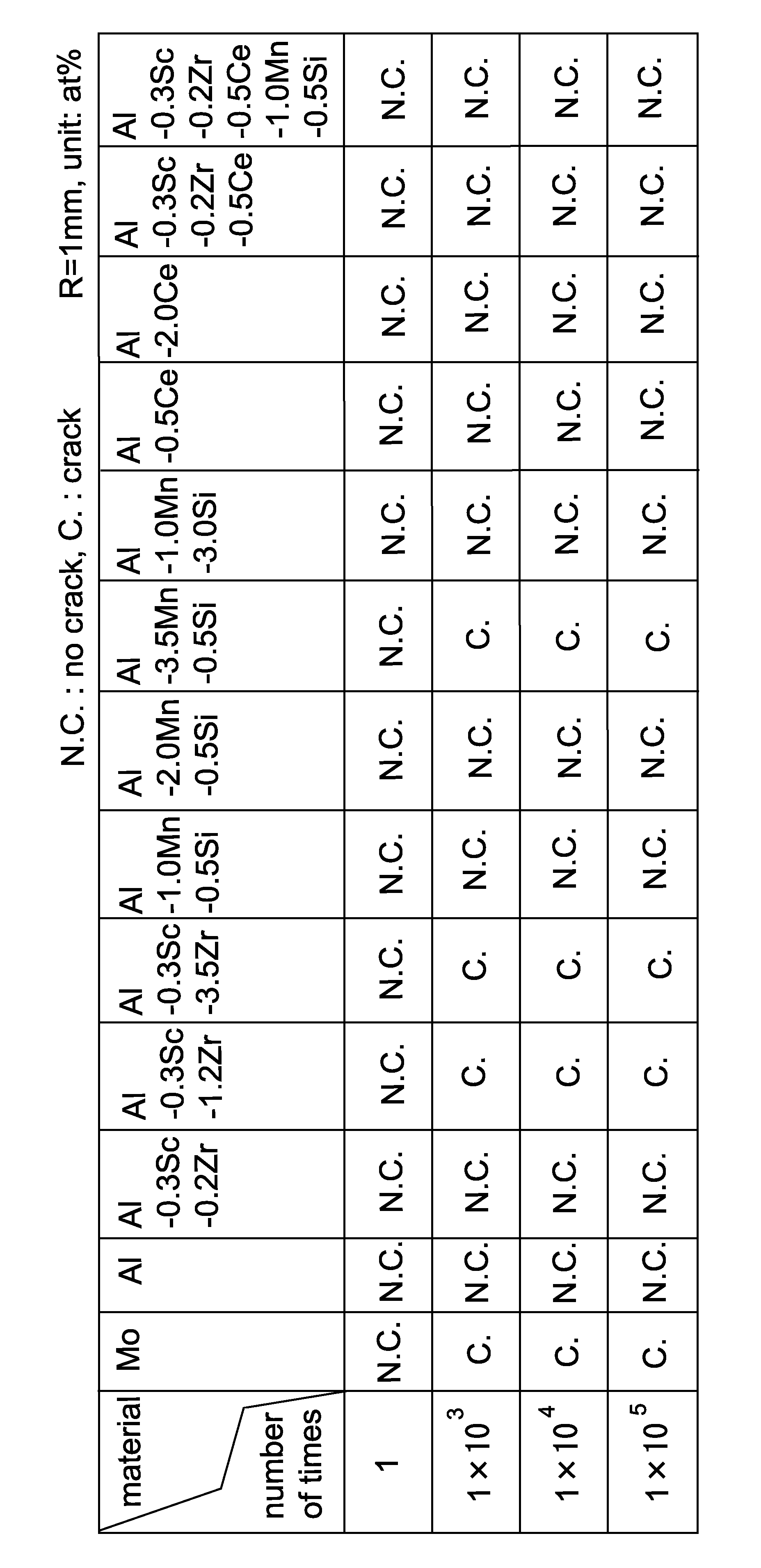
表1には、Mo膜、Al膜、及びAl合金膜の屈曲特性の一例が示されている。濃度の単位は、原子%(at%)である。 Table 1 shows an example of the bending characteristics of the Mo film, the Al film, and the Al alloy film. The unit of the concentration is atomic% (at%).
各サンプルの基板として、2層構造のSiN膜(200nm)/ポリイミド層(25μm)基板を用いた。屈曲試験用のサンプルでは、SiN膜上に、Mo膜、Al膜、及びAl合金膜のそれぞれがスパッタリング成膜されている。屈曲試験での屈曲半径は、1mmである。試験速度は、30rpmである。屈曲回数としては、1回、1000回、10000回、100000回の順に行った。クラックの有無は、光学顕微鏡の画像から目視で判断した。 (4) As a substrate of each sample, a two-layered SiN film (200 nm) / polyimide layer (25 μm) substrate was used. In the sample for the bending test, each of the Mo film, the Al film, and the Al alloy film is formed by sputtering on the SiN film. The bending radius in the bending test is 1 mm. The test speed is 30 rpm. The bending was performed in the order of once, 1,000 times, 10,000 times, and 100,000 times. The presence or absence of cracks was visually determined from the image of the optical microscope.
表1に示すように、Al膜では、100000回までの屈曲回数でクラックが発生しないものの、Mo膜では、1000回の屈曲回数でクラックが発生している。Al合金膜については、100000回までの屈曲回数でクラックが発生しなかった。但し、Al純金属に、第1添加元素を1.0at%よりも高く、1.5at%添加した場合(Al-1.2at%Zr-0.3at%Sc)と、第2添加元素を3.0at%よりも高く、4.0at%添加した場合(Al-3.5at%Mn-0.5at%Si)には、1000回の屈曲回数で、それぞれクラックが発生した。 As shown in Table 1, cracks do not occur in the Al film up to 100,000 bending times, but cracks occur in the Mo film at 1000 bending times. As for the Al alloy film, no crack occurred at the number of bending times up to 100,000. However, when the first additive element is higher than 1.0 at% and added at 1.5 at% (Al-1.2 at% Zr-0.3 at% Sc) to the Al pure metal, the second additive element is added at 3%. When the content was higher than 0.0 at% and 4.0 at% was added (Al-3.5 at% Mn-0.5 at% Si), cracks were generated at 1000 bending times.
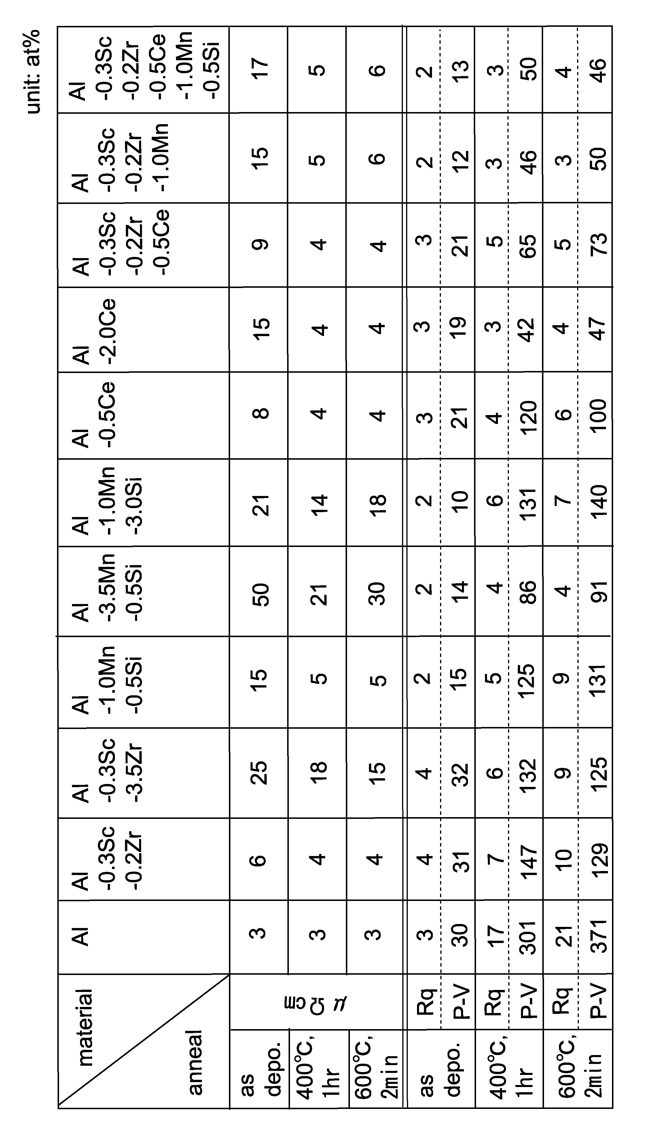
表2には、Al膜及びAl合金膜の比抵抗(μΩ・cm)及び表面粗さ(nm)の一例が示されている。
表2に示すように、Al純金属に、Sc、Zrの第1添加元素が0.01at%以上1.0at%以下含有されているときに、Al合金膜の比抵抗が10μΩ・cm以下になることが分かる。また、Al純金属に、Mn、Siの第2添加元素が0.2at%以上3.0at%以下含有されているときにも、Al合金膜の比抵抗が10μΩ・cm以下になることが分かる。
Table 2 shows an example of the specific resistance (μΩ · cm) and the surface roughness (nm) of the Al film and the Al alloy film.
As shown in Table 2, when the Al pure metal contains the first additive element of Sc and Zr in an amount of 0.01 at% or more and 1.0 at% or less, the specific resistance of the Al alloy film becomes 10 μΩ · cm or less. It turns out that it becomes. It is also found that the specific resistance of the Al alloy film becomes 10 μΩ · cm or less even when the second pure element of Mn and Si is contained in the Al pure metal at 0.2 at% or more and 3.0 at% or less. .
また、表面粗さは、AFM(Atomic Force Microscopy)により測定される。表面粗さの観測は、成膜直後(As Depo.)と、400℃で1時間後と、600℃で2分間後に行っている。測定範囲は、5μm角である。各欄の上段には、Rq値(nm)が示され、下段には、P-V値(nm)が示されている。ここで、Rq値は、二乗平均平方根高さであり、P-V値は、最大高所(peak)と最低低所(valley)との差である。ヒロックが成長するほど、P-V値は、高くなる傾向にある。信頼性の高い表示デバイスを製造するには、配線膜のP-V値がより小さいことが好ましく、好ましくは、50nm以下であることが望ましい。特に、表示パネルの屈曲部分にP-V値が50nm以下のAl合金膜を適用することで、Al合金膜が曲げられたとしても、Al合金膜の上層との密着が良好になる。 表面 The surface roughness is measured by AFM (Atomic Force Microscopy). The surface roughness was observed immediately after film formation (As @ Depo.), After one hour at 400 ° C., and after two minutes at 600 ° C. The measurement range is 5 μm square. The upper row of each column shows the Rq value (nm), and the lower row shows the PV value (nm). Here, the Rq value is the root mean square height, and the PV value is the difference between the maximum height (peak) and the minimum height (valley). As the hillock grows, the PV value tends to increase. In order to manufacture a highly reliable display device, the PV value of the wiring film is preferably smaller, and more preferably, 50 nm or less. In particular, by applying an Al alloy film having a PV value of 50 nm or less to the bent portion of the display panel, even if the Al alloy film is bent, the adhesion with the upper layer of the Al alloy film is improved.
表2に示すように、成膜直後では、Al膜、Al合金膜は、いずれも表面粗さが50nm以下になっている。しかし、加熱処理を施した後では、Al膜のP-V値は、300nmを超えている。一方、Al合金膜においては、いずれもAl膜よりもP-V値が小さくなっている。すなわち、Al合金膜では、加熱処理を施してもAl膜に比べて膜中にヒロックが成長しにくい、と判断できる。 As shown in Table 2, immediately after the film formation, the Al film and the Al alloy film both have a surface roughness of 50 nm or less. However, after the heat treatment, the PV value of the Al film exceeds 300 nm. On the other hand, the PV value of the Al alloy film is smaller than that of the Al film. That is, it can be determined that hillocks are less likely to grow in the Al alloy film than in the Al film even after the heat treatment.
特に、Al-0.2at%Zr-0.3at%Sc-1.0at%Mn、Al-0.5at%Ce-0.2at%Zr-0.3at%Sc-1.0at%Mn-0.5at%Siのように、Al純金属に、第1添加元素と第2添加元素をともに添加することにより、加熱処理を施しても、表面粗さP-V値が50nm以下になることが分かった。これは、Al合金膜において、第1添加元素と第2添加元素とが相乗的に作用し、Al合金膜が熱負荷に対しての優れた耐性を備えている、と考えられる。 In particular, Al-0.2at% Zr-0.3at% Sc-1.0at% Mn, Al-0.5at% Ce-0.2at% Zr-0.3at% Sc-1.0at% Mn-0. By adding both the first additive element and the second additive element to the Al pure metal like 5 at% Si, it can be seen that the surface roughness PV value becomes 50 nm or less even when heat treatment is performed. Was. This is presumably because in the Al alloy film, the first additive element and the second additive element act synergistically, and the Al alloy film has excellent resistance to a thermal load.

表3には、Al膜及びAl合金膜のエッチング後における残渣の有無の一例が示されている。 Table 3 shows an example of the presence or absence of a residue after the etching of the Al film and the Al alloy film.
ドライエッチングにおいて、エッチングガスは、Cl2(50sccm)/Ar(20sccm)の混合ガスである。エッチング圧は、1.0Paである。放電電力は、基板バイアス電力が200Wの状態で、400Wである。ウェットエッチング液としては、リン酸/硝酸/酢酸/水の混合溶液(通称、PAN)が用いられている。液温は、40℃である。 In dry etching, an etching gas is a mixed gas of Cl 2 (50 sccm) / Ar (20 sccm). The etching pressure is 1.0 Pa. The discharge power is 400 W when the substrate bias power is 200 W. As the wet etching solution, a mixed solution of phosphoric acid / nitric acid / acetic acid / water (commonly referred to as PAN) is used. The liquid temperature is 40 ° C.
表3に示すように、第3添加元素であるCeが0.5at%含まれたAl合金膜(Al-0.5at%Ce、Al-0.3at%Sc-0.2at%Zr-0.5at%Ce、Al-0.3at%Sc-0.2at%Zr-0.5at%Ce-1.0at%Mn-0.5at%Si)では、いずれも残渣なくドライエッチング及びウェットエッチングが可能になっている。一方、Ceの濃度が高くなり、Ceが2.0at%のAl合金膜(Al-2.0at%Ce)では、ドライエッチングで残渣が生じた。 As shown in Table 3, an Al alloy film containing 0.5 at% of Ce as the third additive element (Al-0.5 at% Ce, Al-0.3 at% Sc-0.2 at% Zr-0. 5at% Ce, Al-0.3at% Sc-0.2at% Zr-0.5at% Ce-1.0at% Mn-0.5at% Si) enables dry etching and wet etching without any residue Has become. On the other hand, the concentration of Ce increased, and in the Al alloy film with 2.0 at% Ce (Al-2.0 at% Ce), residues were generated by dry etching.
なお、ドライエッチング及びウェットエッチングではともに、Al-0.3at%Sc-0.2at%Zrと、Al-0.3at%Sc-3.5at%Zrとを比較した場合、Zrの含有量が多いAl-0.3at%Sc-3.5at%Zrでは、残渣が生じることが分かった。また、ドライエッチングでは、Al-1.0at%Mn-0.5at%Siと、Al-3.5at%Mn-0.5at%Siとを比較した場合、Mnの含有量が多いAl-3.5at%Mn-0.5at%Siでは残渣が生じることが分かった。一方、ウェットエッチングでは、Al-1.0at%Mn-0.5at%Siと、Al-1.0at%Mn-3.0at%Siとを比較した場合、Siの含有量が多いAl-1.0at%Mn-3.0at%Siでは残渣が生じることが分かった。 In both the dry etching and the wet etching, when comparing Al-0.3 at% Sc-0.2 at% Zr with Al-0.3 at% Sc-3.5 at% Zr, the content of Zr is large. It was found that a residue was generated with Al-0.3 at% Sc-3.5 at% Zr. In dry etching, when comparing Al-1.0 at% Mn-0.5 at% Si with Al-3.5 at% Mn-0.5 at% Si, Al-3. It was found that a residue was generated with 5 at% Mn-0.5 at% Si. On the other hand, in the wet etching, when comparing Al-1.0 at% Mn-0.5 at% Si with Al-1.0 at% Mn-3.0 at% Si, Al-1. It was found that residues were generated at 0 at% Mn and 3.0 at% Si.
(Al合金ターゲットの具体例) (Specific example of Al alloy target)
例えば、坩堝に、Al、Sc、Zr、Mn、Si、及びCeそれぞれの金属材料(金属片、金属粉)が設置される。例えば、Al合金ターゲットの添加元素の成分比が0.2at%Sc、0.1at%Zr、1.0at%Mn、0.5at%Si、及び0.5at%Ceとなるように、それぞれの金属材料(金属片、金属粉)が坩堝内に設置される。 For example, metal materials (metal pieces, metal powders) of Al, Sc, Zr, Mn, Si, and Ce are placed in a crucible. For example, each metal is set so that the component ratio of the additive element of the Al alloy target is 0.2 at% Sc, 0.1 at% Zr, 1.0 at% Mn, 0.5 at% Si, and 0.5 at% Ce. Materials (metal pieces, metal powder) are placed in the crucible.
次に、誘導加熱により、Al合金の融点(例えば、640℃)よりも、400℃以上高い溶融温度(例えば、1050℃)に各金属材料が加熱されて、各金属材料が坩堝内で溶融される。次に、この溶融温度から、溶融した金属が室温まで冷却されてアルミニウム合金インゴットが形成される。この後、アルミニウム合金インゴットは、必要に応じて鍛造され、アルミニウム合金インゴットが板状または円板状に切り出される。これにより、Al合金ターゲットが形成される。 Next, by induction heating, each metal material is heated to a melting temperature (for example, 1050 ° C.) higher than the melting point of the Al alloy (for example, 640 ° C.) by 400 ° C., and each metal material is melted in the crucible. You. Next, from this melting temperature, the molten metal is cooled to room temperature to form an aluminum alloy ingot. Thereafter, the aluminum alloy ingot is forged as necessary, and the aluminum alloy ingot is cut into a plate shape or a disk shape. Thereby, an Al alloy target is formed.
ここで、スパッタリングターゲット用の合金インゴットを形成する方法として、金属材料の融点よりも若干高い溶融温度で金属材料を溶融し、その若干高い溶融温度から金属材料が冷却されて、合金インゴットを形成する方法がある。これは、溶融状態から冷却されるまでの冷却時間を短くすることにより、冷却過程で生じる金属間化合物の析出を避けるためである。しかし、この方法では、溶融温度が融点よりも若干高い温度に設定されることから、金属材料が充分に混合しなくなる可能性がある。 Here, as a method of forming an alloy ingot for a sputtering target, a metal material is melted at a melting temperature slightly higher than the melting point of the metal material, and the metal material is cooled from the slightly higher melting temperature to form an alloy ingot. There is a way. This is to prevent the precipitation of intermetallic compounds generated in the cooling process by shortening the cooling time from the molten state to cooling. However, in this method, since the melting temperature is set to a temperature slightly higher than the melting point, the metal material may not be sufficiently mixed.
これに対して、本実施例では、Al合金の融点よりも、400℃以上高い溶融温度で金属材料が加熱溶融されるため、それぞれの金属材料が充分に混合しあうことになる。ここで、溶融温度が高くなるほど、溶融温度から室温までの冷却時間が長くなり、金属間化合物が析出しやすくなるとも考えられる。しかし、本実施形態では、このようなAl合金の融点よりも400℃以上高い溶融温度からAl合金インゴットが冷却されても、Al合金インゴット中に、金属間化合物が析出しにくくなるように、添加元素の濃度が調整されている。 On the other hand, in this embodiment, since the metal materials are heated and melted at a melting temperature higher than the melting point of the Al alloy by 400 ° C. or more, the respective metal materials are sufficiently mixed. Here, it is considered that the higher the melting temperature, the longer the cooling time from the melting temperature to room temperature, and the more easily the intermetallic compound is precipitated. However, in this embodiment, even if the Al alloy ingot is cooled from a melting temperature higher than the melting point of the Al alloy by 400 ° C. or more, the intermetallic compound is hardly precipitated in the Al alloy ingot. The element concentration has been adjusted.
図2は、表4に例示したAl合金インゴットの組成分析の観測点を説明する概念図である。
表4は、Al合金インゴットに含まれる各元素の濃度分布の一例が示されている。
FIG. 2 is a conceptual diagram illustrating observation points in the composition analysis of the Al alloy ingot exemplified in Table 4.
Table 4 shows an example of the concentration distribution of each element contained in the Al alloy ingot.

図2には、例えば、円柱状のAl合金インゴット(100mm径×50mmt)を2つに分割した半円柱状のAl合金インゴット5が例示されている。
FIG. 2 illustrates, for example, a semi-cylindrical
Al合金インゴット5における組成分析の観測点としては、topの位置で横方向に等間隔に9点、middleの位置で横方向に等間隔に9点、及びbottomの位置で横方向に等間隔に9点の計27点が選択されている。表4には、topの位置での各元素の9点の観測点から測定された平均値濃度(at%)と、middleの位置での各元素の9点の観測点から測定された平均値濃度(at%)と、bottomの位置での各元素の9点の観測点から測定された平均値濃度(at%)が示されている。表4には、濃度の平均値の偏差±3σも示されている。
As observation points of the composition analysis in the
表4に示すように、Al合金インゴットの添加元素の成分比は、top、middle、及びbottomのいずれの位置でも、Scが0.2at%、Zrが0.1at%、Mnが1.0at%、Siが0.5at%、Ceが0.5at%程度になっており、Al合金インゴットにおいて、それぞれの金属材料がAl合金インゴットの縦方向及び横方向で均一に分散されていることが分かる。 As shown in Table 4, the composition ratio of the additive elements of the Al alloy ingot was such that Sc was 0.2 at%, Zr was 0.1 at%, and Mn was 1.0 at% at any position of top, middle, and bottom. , Si is about 0.5 at% and Ce is about 0.5 at%, and it can be seen that in the Al alloy ingot, the respective metal materials are uniformly dispersed in the longitudinal direction and the lateral direction of the Al alloy ingot.
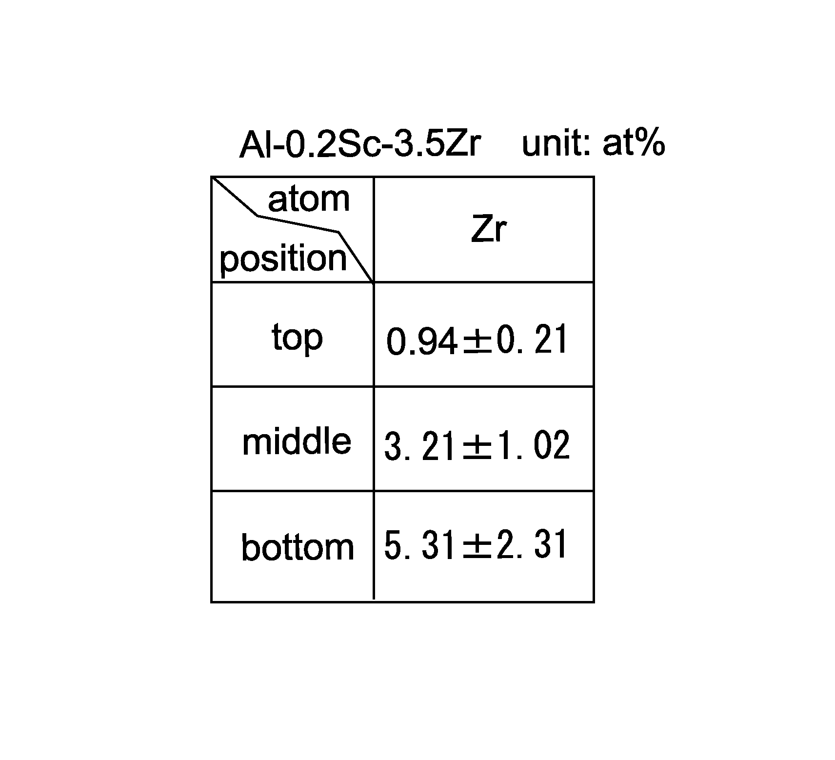
これに対して、表5に、Scを0.2at%、Zrを3.5at%添加させた場合のアルミ合金インゴットのZr濃度分布を示す。製造方法は、表4に示すアルミ合金インゴットと同じである。表5に示すように、Zr濃度を3.5at%まで増加させると、アルミ合金インゴットのtopからbottomに向かうにつれ、Zr濃度が高くなっていることが分かった。この場合の電子顕微鏡像を図3に示す。 On the other hand, Table 5 shows the Zr concentration distribution of the aluminum alloy ingot when Sc was added at 0.2 at% and Zr was added at 3.5 at%. The manufacturing method is the same as the aluminum alloy ingot shown in Table 4. As shown in Table 5, when the Zr concentration was increased to 3.5 at%, it was found that the Zr concentration increased from the top to the bottom of the aluminum alloy ingot. An electron microscope image in this case is shown in FIG.
図3は、表5に示されたアルミ合金インゴットの光学顕微鏡像である。 FIG. 3 is an optical microscope image of the aluminum alloy ingot shown in Table 5.
図3に示すように、表5に示されたアルミ合金インゴット中には、粒径が数100μm程度の結晶粒(金属間化合物)が存在することが分かった。 よ う As shown in FIG. 3, it was found that crystal grains (intermetallic compounds) having a grain size of about several hundred μm existed in the aluminum alloy ingot shown in Table 5.
図4(a)、(b)は、本実施形態に係るアルミ合金インゴットの電子顕微鏡像である。 FIGS. 4A and 4B are electron microscope images of the aluminum alloy ingot according to the present embodiment.
図4(a)には、表4で示されたアルミ合金インゴットの表面電子顕微鏡像が示されている。また、図4(b)には、表4で示されたアルミ合金インゴットに600℃、2時間の加熱処理を行った後のアルミ合金インゴットの表面電子顕微鏡像が示されている。図4(a)、(b)における右の像は、左の像のスケールを拡大した像である。 FIG. 4A shows a surface electron microscope image of the aluminum alloy ingot shown in Table 4. FIG. 4B shows a surface electron microscope image of the aluminum alloy ingot shown in Table 4 after heat treatment at 600 ° C. for 2 hours. The right images in FIGS. 4A and 4B are images obtained by enlarging the scale of the left image.
図4(a)左に示されるように、アルミ合金インゴットを作製した直後では、粒径が数100μm程度の結晶粒(金属間化合物)は観察されていない。但し、図4(a)右に示されるように、アルミ合金インゴットが平均粒径10μm程度の粒子Aの集まりで構成されていた。そして、粒子A間の粒界Bの成分をEDX分析で解析すると、粒界Bでは、Ce、Mn、及びSiが高い濃度で観測された。つまり、粒子A間の粒界におけるCe、Mn、及びSiの少なくともいずれかの含有量は、粒子A内におけるCe、Mn、及びSiの少なくともいずれかの含有量よりも高くなっていることが分かった。 結晶 As shown on the left side of FIG. 4 (a), immediately after the production of the aluminum alloy ingot, no crystal grains (intermetallic compounds) having a grain size of about several 100 μm were observed. However, as shown on the right side of FIG. 4A, the aluminum alloy ingot was composed of a group of particles A having an average particle diameter of about 10 μm. When the components of the grain boundary B between the particles A were analyzed by EDX analysis, Ce, Mn, and Si were observed at a high concentration at the grain boundary B. That is, it is found that the content of at least one of Ce, Mn, and Si in the grain boundary between the particles A is higher than the content of at least one of Ce, Mn, and Si in the particle A. Was.
また、図4(a)の状態から600℃、2時間の加熱処理を行った像を図4(b)に示す。この場合でも粒径は、10μm程度に止まり、粒子A同士が結合して巨大な粒子に成長したり、粒子A内に新たな粒子(例えば、金属間化合物)が析出したりすることはなかった。これは、Al合金インゴットにおいては、粒界Bが障壁となり、隣接する粒子Aが繋がって粒子が粗大化する現象が抑制されたとともに、粒子A内では、Zr、Scが均一に分散され、粒成長が抑制されたと予測できる。この結果、Al合金ターゲットの耐熱性が向上したと考えられる。 {Circle around (2)} FIG. 4 (b) shows an image obtained by performing a heat treatment at 600 ° C. for 2 hours from the state shown in FIG. 4 (a). Even in this case, the particle size is limited to about 10 μm, and the particles A do not combine with each other to grow into a giant particle, and no new particles (for example, an intermetallic compound) are precipitated in the particle A. . This is because, in the Al alloy ingot, the phenomenon that the grain boundary B becomes a barrier and the adjacent particles A are connected and the particles are coarsened is suppressed, and in the particles A, Zr and Sc are uniformly dispersed, It can be predicted that growth was suppressed. As a result, it is considered that the heat resistance of the Al alloy target was improved.
以上、本発明の実施形態について説明したが、本発明は上述の実施形態にのみ限定されるものではなく種々変更を加え得ることは勿論である。各実施形態は、独立の形態とは限らず、技術的に可能な限り複合することができる。 Although the embodiments of the present invention have been described above, the present invention is not limited to the above-described embodiments, and it goes without saying that various modifications can be made. Each embodiment is not limited to an independent form, and can be combined as far as technically possible.
例えば、以上の実施形態では、Al合金膜をゲート電極13、23に適用する例を示したが、Al合金膜をソース・ドレイン電極、ソース・ドレイン電極以外の他の電極、または配線に適用することも可能である。
For example, in the above embodiments, the example in which the Al alloy film is applied to the
1、2…薄膜トランジスタ
10、20…ガラス基板
11、21…活性層
12、22…ゲート絶縁膜
13、23…ゲート電極
15…保護層
15D、25D…ドレイン電極
16S、26S…ソース電極
1, 2
Claims (11)
前記第1添加元素の含有量が0.01原子%以上1.0原子%以下である
アルミニウム合金膜。 Al pure metal contains at least one first additive element selected from the group consisting of Zr, Sc, Mo, Y, Nb, and Ti;
An aluminum alloy film in which the content of the first additive element is 0.01 atomic% or more and 1.0 atomic% or less.
前記第2添加元素の含有量が0.2原子%以上3.0原子%以下である
アルミニウム合金膜。 The aluminum alloy film according to claim 1, further comprising at least one second additive element selected from the group consisting of Mn, Si, Cu, Ge, Mg, Ag, and Ni,
An aluminum alloy film, wherein the content of the second additive element is 0.2 atomic% or more and 3.0 atomic% or less.
前記第2添加元素の含有量が0.2原子%以上3.0原子%以下である
アルミニウム合金膜。 Al pure metal contains at least one second additive element selected from the group consisting of Mn, Si, Cu, Ge, Mg, Ag and Ni,
An aluminum alloy film, wherein the content of the second additive element is 0.2 atomic% or more and 3.0 atomic% or less.
Ce、Nd、La、及びGdの群から選択される少なくとも1種の第3添加元素が含有され、
前記第3添加元素の含有量が0.1原子%以上1.0原子%以下である
アルミニウム合金膜。 The aluminum alloy film according to any one of claims 1 to 3, further comprising:
At least one third additive element selected from the group consisting of Ce, Nd, La, and Gd;
An aluminum alloy film in which the content of the third additive element is 0.1 atomic% or more and 1.0 atomic% or less.
屈曲半径1mmに折り曲げられた場合に耐え得る屈曲耐性を有する
アルミニウム合金膜。 The aluminum alloy film according to any one of claims 1 to 4, wherein
An aluminum alloy film with bending resistance that can withstand bending at a bending radius of 1 mm.
ドライエッチング及びウェットエッチングが可能である
アルミニウム合金膜。 The aluminum alloy film according to any one of claims 1 to 5, wherein
Aluminum alloy film capable of dry etching and wet etching.
表面粗さP-V値が50nm以下である
アルミニウム合金膜。 The aluminum alloy film according to any one of claims 1 to 6, wherein
An aluminum alloy film having a surface roughness PV value of 50 nm or less.
比抵抗が10μΩ・cm以下である
アルミニウム合金膜。 The aluminum alloy film according to any one of claims 1 to 7, wherein
An aluminum alloy film having a specific resistance of 10 μΩ · cm or less.
Priority Applications (4)
| Application Number | Priority Date | Filing Date | Title |
|---|---|---|---|
| KR1020207037510A KR102549527B1 (en) | 2018-06-28 | 2019-03-28 | Aluminum alloy film, manufacturing method therefor, and thin film transistor |
| CN201980039161.2A CN112262222B (en) | 2018-06-28 | 2019-03-28 | Aluminum alloy film, method for producing same, and thin film transistor |
| JP2019547523A JP6842562B2 (en) | 2018-06-28 | 2019-03-28 | Aluminum alloy film, its manufacturing method, and thin film transistor |
| US17/055,852 US11935936B2 (en) | 2018-06-28 | 2019-03-28 | Aluminum alloy film, method of producing the same, and thin film transistor |
Applications Claiming Priority (2)
| Application Number | Priority Date | Filing Date | Title |
|---|---|---|---|
| JP2018123157 | 2018-06-28 | ||
| JP2018-123157 | 2018-06-28 |
Publications (1)
| Publication Number | Publication Date |
|---|---|
| WO2020003667A1 true WO2020003667A1 (en) | 2020-01-02 |
Family
ID=68986972
Family Applications (1)
| Application Number | Title | Priority Date | Filing Date |
|---|---|---|---|
| PCT/JP2019/013570 Ceased WO2020003667A1 (en) | 2018-06-28 | 2019-03-28 | Aluminum alloy film, method for producing same, and thin film transistor |
Country Status (6)
| Country | Link |
|---|---|
| US (1) | US11935936B2 (en) |
| JP (1) | JP6842562B2 (en) |
| KR (1) | KR102549527B1 (en) |
| CN (1) | CN112262222B (en) |
| TW (1) | TWI738005B (en) |
| WO (1) | WO2020003667A1 (en) |
Cited By (3)
| Publication number | Priority date | Publication date | Assignee | Title |
|---|---|---|---|---|
| WO2021206444A1 (en) * | 2020-04-08 | 2021-10-14 | 주식회사 큐프럼 머티리얼즈 | Wiring film manufacturing method, wiring film, and display device comprising same |
| WO2023008475A1 (en) * | 2021-07-30 | 2023-02-02 | 株式会社ニコン | Method for manufacturing metal wiring, method for manufacturing transistor, and metal wiring |
| JP2023173191A (en) * | 2022-05-25 | 2023-12-07 | ルネサスエレクトロニクス株式会社 | Semiconductor device and its manufacturing method |
Families Citing this family (3)
| Publication number | Priority date | Publication date | Assignee | Title |
|---|---|---|---|---|
| JP6735930B2 (en) * | 2018-06-28 | 2020-08-05 | 株式会社アルバック | Aluminum alloy target and manufacturing method thereof |
| KR102865855B1 (en) * | 2021-12-30 | 2025-09-30 | 주식회사 큐프럼 머티리얼즈 | Alloy Composition Comprising Aluminum, Manganese, Titanium and Silicon for Thin Film Transistor Electrodes and Reflective Electrodes |
| WO2024167046A1 (en) * | 2023-02-10 | 2024-08-15 | 주식회사 큐프럼 머티리얼즈 | Thin film transistor electrode, and alloy composition comprising aluminum, manganese, titanium, and silicon for reflective electrode |
Citations (5)
| Publication number | Priority date | Publication date | Assignee | Title |
|---|---|---|---|---|
| JP2004214606A (en) * | 2002-12-19 | 2004-07-29 | Kobe Steel Ltd | Display device, method of manufacturing the same, and sputtering target |
| JP2005171378A (en) * | 2003-11-20 | 2005-06-30 | Hitachi Metals Ltd | Al alloy film for wiring film and sputtering target material for forming wiring film |
| WO2009123217A1 (en) * | 2008-03-31 | 2009-10-08 | 株式会社神戸製鋼所 | Display device, process for producing the display device, and sputtering target |
| JP2011190531A (en) * | 2010-02-16 | 2011-09-29 | Kobe Steel Ltd | Al ALLOY FILM FOR DISPLAY DEVICE |
| JP2012180540A (en) * | 2011-02-28 | 2012-09-20 | Kobe Steel Ltd | Al ALLOY FILM FOR DISPLAY DEVICE AND SEMICONDUCTOR DEVICE |
Family Cites Families (10)
| Publication number | Priority date | Publication date | Assignee | Title |
|---|---|---|---|---|
| JP4137182B2 (en) | 1995-10-12 | 2008-08-20 | 株式会社東芝 | Sputter target for wiring film formation |
| USRE45481E1 (en) * | 1995-10-12 | 2015-04-21 | Kabushiki Kaisha Toshiba | Interconnector line of thin film, sputter target for forming the wiring film and electronic component using the same |
| US20010047838A1 (en) | 2000-03-28 | 2001-12-06 | Segal Vladimir M. | Methods of forming aluminum-comprising physical vapor deposition targets; sputtered films; and target constructions |
| JP4783525B2 (en) * | 2001-08-31 | 2011-09-28 | 株式会社アルバック | Thin film aluminum alloy and sputtering target for forming thin film aluminum alloy |
| JP4237479B2 (en) | 2002-12-25 | 2009-03-11 | 株式会社東芝 | Sputtering target, Al alloy film and electronic parts |
| US7166921B2 (en) | 2003-11-20 | 2007-01-23 | Hitachi Metals, Ltd. | Aluminum alloy film for wiring and sputter target material for forming the film |
| JP5032687B2 (en) * | 2010-09-30 | 2012-09-26 | 株式会社神戸製鋼所 | Al alloy film, wiring structure having Al alloy film, and sputtering target used for production of Al alloy film |
| JP5524905B2 (en) | 2011-05-17 | 2014-06-18 | 株式会社神戸製鋼所 | Al alloy film for power semiconductor devices |
| US9803283B1 (en) * | 2013-10-18 | 2017-10-31 | Hrl Laboratories, Llc | Method of electroless deposition of aluminum or aluminum alloy, an electroless plating composition, and an article including the same |
| CN105917450A (en) | 2014-01-15 | 2016-08-31 | 株式会社神户制钢所 | Thin-film transistor |
-
2019
- 2019-03-28 WO PCT/JP2019/013570 patent/WO2020003667A1/en not_active Ceased
- 2019-03-28 CN CN201980039161.2A patent/CN112262222B/en active Active
- 2019-03-28 JP JP2019547523A patent/JP6842562B2/en active Active
- 2019-03-28 US US17/055,852 patent/US11935936B2/en active Active
- 2019-03-28 KR KR1020207037510A patent/KR102549527B1/en active Active
- 2019-06-14 TW TW108120573A patent/TWI738005B/en active
Patent Citations (5)
| Publication number | Priority date | Publication date | Assignee | Title |
|---|---|---|---|---|
| JP2004214606A (en) * | 2002-12-19 | 2004-07-29 | Kobe Steel Ltd | Display device, method of manufacturing the same, and sputtering target |
| JP2005171378A (en) * | 2003-11-20 | 2005-06-30 | Hitachi Metals Ltd | Al alloy film for wiring film and sputtering target material for forming wiring film |
| WO2009123217A1 (en) * | 2008-03-31 | 2009-10-08 | 株式会社神戸製鋼所 | Display device, process for producing the display device, and sputtering target |
| JP2011190531A (en) * | 2010-02-16 | 2011-09-29 | Kobe Steel Ltd | Al ALLOY FILM FOR DISPLAY DEVICE |
| JP2012180540A (en) * | 2011-02-28 | 2012-09-20 | Kobe Steel Ltd | Al ALLOY FILM FOR DISPLAY DEVICE AND SEMICONDUCTOR DEVICE |
Cited By (4)
| Publication number | Priority date | Publication date | Assignee | Title |
|---|---|---|---|---|
| WO2021206444A1 (en) * | 2020-04-08 | 2021-10-14 | 주식회사 큐프럼 머티리얼즈 | Wiring film manufacturing method, wiring film, and display device comprising same |
| WO2023008475A1 (en) * | 2021-07-30 | 2023-02-02 | 株式会社ニコン | Method for manufacturing metal wiring, method for manufacturing transistor, and metal wiring |
| JP2023173191A (en) * | 2022-05-25 | 2023-12-07 | ルネサスエレクトロニクス株式会社 | Semiconductor device and its manufacturing method |
| US12575428B2 (en) | 2022-05-25 | 2026-03-10 | Renesas Electronics Corporation | Semiconductor device and method of manufacturing the same |
Also Published As
| Publication number | Publication date |
|---|---|
| JP6842562B2 (en) | 2021-03-17 |
| TW202000941A (en) | 2020-01-01 |
| CN112262222B (en) | 2023-06-06 |
| US11935936B2 (en) | 2024-03-19 |
| US20210226028A1 (en) | 2021-07-22 |
| CN112262222A (en) | 2021-01-22 |
| KR20210013220A (en) | 2021-02-03 |
| KR102549527B1 (en) | 2023-06-28 |
| JPWO2020003667A1 (en) | 2020-07-02 |
| TWI738005B (en) | 2021-09-01 |
Similar Documents
| Publication | Publication Date | Title |
|---|---|---|
| JP6842562B2 (en) | Aluminum alloy film, its manufacturing method, and thin film transistor | |
| CN100392505C (en) | Copper alloy film, copper alloy sputtering target and flat panel display | |
| CN1479802A (en) | Aluminum alloy thin film, wiring circuit having the thin film, and target material for forming the thin film | |
| JP6735930B2 (en) | Aluminum alloy target and manufacturing method thereof | |
| WO2012157688A1 (en) | Al ALLOY FILM FOR SEMICONDUCTOR DEVICES | |
| JP6475997B2 (en) | Wiring film for flat panel display and Al alloy sputtering target | |
| JP7133727B2 (en) | Metal wiring structure and method for manufacturing metal wiring structure | |
| KR102677079B1 (en) | Aluminum alloy target, aluminum alloy wiring film, and method of manufacturing aluminum alloy wiring film | |
| JP6947604B2 (en) | Method for manufacturing Al alloy conductive film, thin film transistor and Al alloy conductive film | |
| JP5510812B2 (en) | Cu alloy film for wiring film and sputtering target material for forming wiring film | |
| JP6331824B2 (en) | Copper alloy sputtering target |
Legal Events
| Date | Code | Title | Description |
|---|---|---|---|
| ENP | Entry into the national phase |
Ref document number: 2019547523 Country of ref document: JP Kind code of ref document: A |
|
| 121 | Ep: the epo has been informed by wipo that ep was designated in this application |
Ref document number: 19825256 Country of ref document: EP Kind code of ref document: A1 |
|
| ENP | Entry into the national phase |
Ref document number: 20207037510 Country of ref document: KR Kind code of ref document: A |
|
| NENP | Non-entry into the national phase |
Ref country code: DE |
|
| 122 | Ep: pct application non-entry in european phase |
Ref document number: 19825256 Country of ref document: EP Kind code of ref document: A1 |